EP0952569A2 - Méthode de commande d'un panneau d'affichage à plasma - Google Patents
Méthode de commande d'un panneau d'affichage à plasma Download PDFInfo
- Publication number
- EP0952569A2 EP0952569A2 EP99107909A EP99107909A EP0952569A2 EP 0952569 A2 EP0952569 A2 EP 0952569A2 EP 99107909 A EP99107909 A EP 99107909A EP 99107909 A EP99107909 A EP 99107909A EP 0952569 A2 EP0952569 A2 EP 0952569A2
- Authority
- EP
- European Patent Office
- Prior art keywords
- pixel data
- subfields
- discharge
- light emitting
- stage
- Prior art date
- Legal status (The legal status is an assumption and is not a legal conclusion. Google has not performed a legal analysis and makes no representation as to the accuracy of the status listed.)
- Withdrawn
Links
Images


















Classifications
-
- G—PHYSICS
- G09—EDUCATION; CRYPTOGRAPHY; DISPLAY; ADVERTISING; SEALS
- G09G—ARRANGEMENTS OR CIRCUITS FOR CONTROL OF INDICATING DEVICES USING STATIC MEANS TO PRESENT VARIABLE INFORMATION
- G09G3/00—Control arrangements or circuits, of interest only in connection with visual indicators other than cathode-ray tubes
- G09G3/20—Control arrangements or circuits, of interest only in connection with visual indicators other than cathode-ray tubes for presentation of an assembly of a number of characters, e.g. a page, by composing the assembly by combination of individual elements arranged in a matrix no fixed position being assigned to or needed to be assigned to the individual characters or partial characters
- G09G3/2007—Display of intermediate tones
- G09G3/2059—Display of intermediate tones using error diffusion
-
- G—PHYSICS
- G09—EDUCATION; CRYPTOGRAPHY; DISPLAY; ADVERTISING; SEALS
- G09G—ARRANGEMENTS OR CIRCUITS FOR CONTROL OF INDICATING DEVICES USING STATIC MEANS TO PRESENT VARIABLE INFORMATION
- G09G3/00—Control arrangements or circuits, of interest only in connection with visual indicators other than cathode-ray tubes
- G09G3/20—Control arrangements or circuits, of interest only in connection with visual indicators other than cathode-ray tubes for presentation of an assembly of a number of characters, e.g. a page, by composing the assembly by combination of individual elements arranged in a matrix no fixed position being assigned to or needed to be assigned to the individual characters or partial characters
- G09G3/2007—Display of intermediate tones
- G09G3/2018—Display of intermediate tones by time modulation using two or more time intervals
- G09G3/2022—Display of intermediate tones by time modulation using two or more time intervals using sub-frames
-
- G—PHYSICS
- G09—EDUCATION; CRYPTOGRAPHY; DISPLAY; ADVERTISING; SEALS
- G09G—ARRANGEMENTS OR CIRCUITS FOR CONTROL OF INDICATING DEVICES USING STATIC MEANS TO PRESENT VARIABLE INFORMATION
- G09G3/00—Control arrangements or circuits, of interest only in connection with visual indicators other than cathode-ray tubes
- G09G3/20—Control arrangements or circuits, of interest only in connection with visual indicators other than cathode-ray tubes for presentation of an assembly of a number of characters, e.g. a page, by composing the assembly by combination of individual elements arranged in a matrix no fixed position being assigned to or needed to be assigned to the individual characters or partial characters
- G09G3/2007—Display of intermediate tones
- G09G3/2044—Display of intermediate tones using dithering
- G09G3/2051—Display of intermediate tones using dithering with use of a spatial dither pattern
-
- G—PHYSICS
- G09—EDUCATION; CRYPTOGRAPHY; DISPLAY; ADVERTISING; SEALS
- G09G—ARRANGEMENTS OR CIRCUITS FOR CONTROL OF INDICATING DEVICES USING STATIC MEANS TO PRESENT VARIABLE INFORMATION
- G09G3/00—Control arrangements or circuits, of interest only in connection with visual indicators other than cathode-ray tubes
- G09G3/20—Control arrangements or circuits, of interest only in connection with visual indicators other than cathode-ray tubes for presentation of an assembly of a number of characters, e.g. a page, by composing the assembly by combination of individual elements arranged in a matrix no fixed position being assigned to or needed to be assigned to the individual characters or partial characters
- G09G3/22—Control arrangements or circuits, of interest only in connection with visual indicators other than cathode-ray tubes for presentation of an assembly of a number of characters, e.g. a page, by composing the assembly by combination of individual elements arranged in a matrix no fixed position being assigned to or needed to be assigned to the individual characters or partial characters using controlled light sources
- G09G3/28—Control arrangements or circuits, of interest only in connection with visual indicators other than cathode-ray tubes for presentation of an assembly of a number of characters, e.g. a page, by composing the assembly by combination of individual elements arranged in a matrix no fixed position being assigned to or needed to be assigned to the individual characters or partial characters using controlled light sources using luminous gas-discharge panels, e.g. plasma panels
- G09G3/288—Control arrangements or circuits, of interest only in connection with visual indicators other than cathode-ray tubes for presentation of an assembly of a number of characters, e.g. a page, by composing the assembly by combination of individual elements arranged in a matrix no fixed position being assigned to or needed to be assigned to the individual characters or partial characters using controlled light sources using luminous gas-discharge panels, e.g. plasma panels using AC panels
- G09G3/291—Control arrangements or circuits, of interest only in connection with visual indicators other than cathode-ray tubes for presentation of an assembly of a number of characters, e.g. a page, by composing the assembly by combination of individual elements arranged in a matrix no fixed position being assigned to or needed to be assigned to the individual characters or partial characters using controlled light sources using luminous gas-discharge panels, e.g. plasma panels using AC panels controlling the gas discharge to control a cell condition, e.g. by means of specific pulse shapes
- G09G3/292—Control arrangements or circuits, of interest only in connection with visual indicators other than cathode-ray tubes for presentation of an assembly of a number of characters, e.g. a page, by composing the assembly by combination of individual elements arranged in a matrix no fixed position being assigned to or needed to be assigned to the individual characters or partial characters using controlled light sources using luminous gas-discharge panels, e.g. plasma panels using AC panels controlling the gas discharge to control a cell condition, e.g. by means of specific pulse shapes for reset discharge, priming discharge or erase discharge occurring in a phase other than addressing
- G09G3/2922—Details of erasing
-
- G—PHYSICS
- G09—EDUCATION; CRYPTOGRAPHY; DISPLAY; ADVERTISING; SEALS
- G09G—ARRANGEMENTS OR CIRCUITS FOR CONTROL OF INDICATING DEVICES USING STATIC MEANS TO PRESENT VARIABLE INFORMATION
- G09G3/00—Control arrangements or circuits, of interest only in connection with visual indicators other than cathode-ray tubes
- G09G3/20—Control arrangements or circuits, of interest only in connection with visual indicators other than cathode-ray tubes for presentation of an assembly of a number of characters, e.g. a page, by composing the assembly by combination of individual elements arranged in a matrix no fixed position being assigned to or needed to be assigned to the individual characters or partial characters
- G09G3/22—Control arrangements or circuits, of interest only in connection with visual indicators other than cathode-ray tubes for presentation of an assembly of a number of characters, e.g. a page, by composing the assembly by combination of individual elements arranged in a matrix no fixed position being assigned to or needed to be assigned to the individual characters or partial characters using controlled light sources
- G09G3/28—Control arrangements or circuits, of interest only in connection with visual indicators other than cathode-ray tubes for presentation of an assembly of a number of characters, e.g. a page, by composing the assembly by combination of individual elements arranged in a matrix no fixed position being assigned to or needed to be assigned to the individual characters or partial characters using controlled light sources using luminous gas-discharge panels, e.g. plasma panels
- G09G3/288—Control arrangements or circuits, of interest only in connection with visual indicators other than cathode-ray tubes for presentation of an assembly of a number of characters, e.g. a page, by composing the assembly by combination of individual elements arranged in a matrix no fixed position being assigned to or needed to be assigned to the individual characters or partial characters using controlled light sources using luminous gas-discharge panels, e.g. plasma panels using AC panels
- G09G3/291—Control arrangements or circuits, of interest only in connection with visual indicators other than cathode-ray tubes for presentation of an assembly of a number of characters, e.g. a page, by composing the assembly by combination of individual elements arranged in a matrix no fixed position being assigned to or needed to be assigned to the individual characters or partial characters using controlled light sources using luminous gas-discharge panels, e.g. plasma panels using AC panels controlling the gas discharge to control a cell condition, e.g. by means of specific pulse shapes
- G09G3/292—Control arrangements or circuits, of interest only in connection with visual indicators other than cathode-ray tubes for presentation of an assembly of a number of characters, e.g. a page, by composing the assembly by combination of individual elements arranged in a matrix no fixed position being assigned to or needed to be assigned to the individual characters or partial characters using controlled light sources using luminous gas-discharge panels, e.g. plasma panels using AC panels controlling the gas discharge to control a cell condition, e.g. by means of specific pulse shapes for reset discharge, priming discharge or erase discharge occurring in a phase other than addressing
- G09G3/2927—Details of initialising
-
- G—PHYSICS
- G09—EDUCATION; CRYPTOGRAPHY; DISPLAY; ADVERTISING; SEALS
- G09G—ARRANGEMENTS OR CIRCUITS FOR CONTROL OF INDICATING DEVICES USING STATIC MEANS TO PRESENT VARIABLE INFORMATION
- G09G3/00—Control arrangements or circuits, of interest only in connection with visual indicators other than cathode-ray tubes
- G09G3/20—Control arrangements or circuits, of interest only in connection with visual indicators other than cathode-ray tubes for presentation of an assembly of a number of characters, e.g. a page, by composing the assembly by combination of individual elements arranged in a matrix no fixed position being assigned to or needed to be assigned to the individual characters or partial characters
- G09G3/22—Control arrangements or circuits, of interest only in connection with visual indicators other than cathode-ray tubes for presentation of an assembly of a number of characters, e.g. a page, by composing the assembly by combination of individual elements arranged in a matrix no fixed position being assigned to or needed to be assigned to the individual characters or partial characters using controlled light sources
- G09G3/28—Control arrangements or circuits, of interest only in connection with visual indicators other than cathode-ray tubes for presentation of an assembly of a number of characters, e.g. a page, by composing the assembly by combination of individual elements arranged in a matrix no fixed position being assigned to or needed to be assigned to the individual characters or partial characters using controlled light sources using luminous gas-discharge panels, e.g. plasma panels
- G09G3/288—Control arrangements or circuits, of interest only in connection with visual indicators other than cathode-ray tubes for presentation of an assembly of a number of characters, e.g. a page, by composing the assembly by combination of individual elements arranged in a matrix no fixed position being assigned to or needed to be assigned to the individual characters or partial characters using controlled light sources using luminous gas-discharge panels, e.g. plasma panels using AC panels
- G09G3/291—Control arrangements or circuits, of interest only in connection with visual indicators other than cathode-ray tubes for presentation of an assembly of a number of characters, e.g. a page, by composing the assembly by combination of individual elements arranged in a matrix no fixed position being assigned to or needed to be assigned to the individual characters or partial characters using controlled light sources using luminous gas-discharge panels, e.g. plasma panels using AC panels controlling the gas discharge to control a cell condition, e.g. by means of specific pulse shapes
- G09G3/293—Control arrangements or circuits, of interest only in connection with visual indicators other than cathode-ray tubes for presentation of an assembly of a number of characters, e.g. a page, by composing the assembly by combination of individual elements arranged in a matrix no fixed position being assigned to or needed to be assigned to the individual characters or partial characters using controlled light sources using luminous gas-discharge panels, e.g. plasma panels using AC panels controlling the gas discharge to control a cell condition, e.g. by means of specific pulse shapes for address discharge
- G09G3/2935—Addressed by erasing selected cells that are in an ON state
-
- G—PHYSICS
- G09—EDUCATION; CRYPTOGRAPHY; DISPLAY; ADVERTISING; SEALS
- G09G—ARRANGEMENTS OR CIRCUITS FOR CONTROL OF INDICATING DEVICES USING STATIC MEANS TO PRESENT VARIABLE INFORMATION
- G09G3/00—Control arrangements or circuits, of interest only in connection with visual indicators other than cathode-ray tubes
- G09G3/20—Control arrangements or circuits, of interest only in connection with visual indicators other than cathode-ray tubes for presentation of an assembly of a number of characters, e.g. a page, by composing the assembly by combination of individual elements arranged in a matrix no fixed position being assigned to or needed to be assigned to the individual characters or partial characters
- G09G3/22—Control arrangements or circuits, of interest only in connection with visual indicators other than cathode-ray tubes for presentation of an assembly of a number of characters, e.g. a page, by composing the assembly by combination of individual elements arranged in a matrix no fixed position being assigned to or needed to be assigned to the individual characters or partial characters using controlled light sources
- G09G3/28—Control arrangements or circuits, of interest only in connection with visual indicators other than cathode-ray tubes for presentation of an assembly of a number of characters, e.g. a page, by composing the assembly by combination of individual elements arranged in a matrix no fixed position being assigned to or needed to be assigned to the individual characters or partial characters using controlled light sources using luminous gas-discharge panels, e.g. plasma panels
- G09G3/288—Control arrangements or circuits, of interest only in connection with visual indicators other than cathode-ray tubes for presentation of an assembly of a number of characters, e.g. a page, by composing the assembly by combination of individual elements arranged in a matrix no fixed position being assigned to or needed to be assigned to the individual characters or partial characters using controlled light sources using luminous gas-discharge panels, e.g. plasma panels using AC panels
- G09G3/291—Control arrangements or circuits, of interest only in connection with visual indicators other than cathode-ray tubes for presentation of an assembly of a number of characters, e.g. a page, by composing the assembly by combination of individual elements arranged in a matrix no fixed position being assigned to or needed to be assigned to the individual characters or partial characters using controlled light sources using luminous gas-discharge panels, e.g. plasma panels using AC panels controlling the gas discharge to control a cell condition, e.g. by means of specific pulse shapes
- G09G3/293—Control arrangements or circuits, of interest only in connection with visual indicators other than cathode-ray tubes for presentation of an assembly of a number of characters, e.g. a page, by composing the assembly by combination of individual elements arranged in a matrix no fixed position being assigned to or needed to be assigned to the individual characters or partial characters using controlled light sources using luminous gas-discharge panels, e.g. plasma panels using AC panels controlling the gas discharge to control a cell condition, e.g. by means of specific pulse shapes for address discharge
- G09G3/2937—Control arrangements or circuits, of interest only in connection with visual indicators other than cathode-ray tubes for presentation of an assembly of a number of characters, e.g. a page, by composing the assembly by combination of individual elements arranged in a matrix no fixed position being assigned to or needed to be assigned to the individual characters or partial characters using controlled light sources using luminous gas-discharge panels, e.g. plasma panels using AC panels controlling the gas discharge to control a cell condition, e.g. by means of specific pulse shapes for address discharge being addressed only once per frame
-
- G—PHYSICS
- G09—EDUCATION; CRYPTOGRAPHY; DISPLAY; ADVERTISING; SEALS
- G09G—ARRANGEMENTS OR CIRCUITS FOR CONTROL OF INDICATING DEVICES USING STATIC MEANS TO PRESENT VARIABLE INFORMATION
- G09G2320/00—Control of display operating conditions
- G09G2320/02—Improving the quality of display appearance
- G09G2320/0238—Improving the black level
-
- G—PHYSICS
- G09—EDUCATION; CRYPTOGRAPHY; DISPLAY; ADVERTISING; SEALS
- G09G—ARRANGEMENTS OR CIRCUITS FOR CONTROL OF INDICATING DEVICES USING STATIC MEANS TO PRESENT VARIABLE INFORMATION
- G09G2320/00—Control of display operating conditions
- G09G2320/02—Improving the quality of display appearance
- G09G2320/0266—Reduction of sub-frame artefacts
-
- G—PHYSICS
- G09—EDUCATION; CRYPTOGRAPHY; DISPLAY; ADVERTISING; SEALS
- G09G—ARRANGEMENTS OR CIRCUITS FOR CONTROL OF INDICATING DEVICES USING STATIC MEANS TO PRESENT VARIABLE INFORMATION
- G09G2360/00—Aspects of the architecture of display systems
- G09G2360/16—Calculation or use of calculated indices related to luminance levels in display data
Definitions
- the present invention relates to a method of driving a plasma display panel (hereinafter abbreviated as the "PDP") of a matrix display type.
- PDP plasma display panel
- an AC (alternate current discharge) type PDP is known.
- the AC-type PDP comprises a plurality of column electrodes (address electrodes) and a plurality of row electrode pairs arranged orthogonal to the column electrodes, with each pair of row electrodes forming a scanning line.
- the row electrode pairs and column electrodes are covered with a dielectric layer to separate them from a discharge space.
- a discharge cell is formed corresponding to one pixel.
- a so-called subfield method is described, for example, in Japanese Patent Kokai No. 4-195087.
- a field period is divided into N subfields, in each of which light is emitted for a time corresponding to weighting applied to an associated bit of N-bit pixel data.
- Fig. 1 illustrates a light emission driving format in one field period according to the subfield method.
- supplied pixel data is assumed to be 6-bit data, and one field period is divided into six subfields SF1, SF2, ..., SF6 for driving light emission.
- a gradation display of 64 steps can be achieved for an image of one field by executing light emission throughout the six subfields.
- Each subfield includes a simultaneous resetting stage Rc, a pixel data writing stage Wc and a light emission sustaining stage Ic.
- the simultaneous resetting stage Rc all discharge cells in the PDP are simultaneously excited to discharge (reset discharge) to form a wall charge uniformly in each of all discharge cells.
- the next pixel data writing stage Wc a selective erasing discharge is excited in accordance with pixel data in each discharge cell.
- the wall charge in a discharge cell which undergoes the erasure discharge is extinct to become a "non-light emitting cell.”
- a discharge cell which does not undergo the erasure discharge has the wall charge maintained, so that it serves as a "light emitting cell.”
- the light emitting cells are maintained in a discharge light emitting state for a time corresponding to weighting of each subfield. In this way, the emitted light is sustained in the respective subfields SF1 - SF6 in a light emitting period ratio of 1:2:4:8:16:32 in order.
- the simultaneous resetting stage Rc is essentially provided at the head of each subfield.
- the reset discharge performed for all discharge cells in the simultaneous resetting stage Rc involves relatively strong discharge, i.e., emission of light at a high luminance level.
- the reset discharge causes light emission at the six times indicated by hatchings in Fig. 1 without any relation to pixel data, this results in a problem of degraded contrast in images.
- a discharge cell which emits light at a luminance level 31 has a light emitting pattern reverse to that of a discharge cell which emits light at a luminance level 32.
- one cell is emitting light, while the other cell is not, thus causing a problem that a pseudo-contour is formed on the boundary of the two discharge cells.
- the present invention has been made to solve the problems mentioned above, and its object is to provide a method of driving a plasma display panel which is capable of improving contract, reducing power consumption, and preventing a pseudo-contour.
- the present invention provides a method of driving a plasma display panel for driving a plasma display panel having a discharge cell corresponding to one pixel at each intersection of each of a plurality of row electrodes arranged to form each scanning line with each of a plurality of column electrodes crossing with the row electrodes, and the method comprises the steps of dividing a display period of one field into a plurality of subfields, and executing, in each of the subfields, a pixel data writing stage for selectively erasing or discharging a wall charge formed in each of the discharge cells in accordance with display pixel data to set the discharge cells to a light emitting cell or a non-light emitting cell, and a light emission sustaining stage for sustaining only the light emitting cells to emit light for a time corresponding to weighting to the subfield, and executing a simultaneous resetting stage for simultaneously resetting to discharge all the discharge cells to form a wall charge in each of the discharge cells only in the first subfield of a group of subfields
- the display period of one field is divided to N (N is a natural number) subfields, and a subfield group of consecutive M (2 ⁇ M ⁇ N) subfields is formed.
- the method executes in order, a resetting stage for producing a discharge to initialize all of the discharge cells to a state of either of a light emitting cell or a non-light emitting cell only in the subfields in the head portion of the subfield group, a pixel data writing stage for applying to the column electrodes a first pixel data pulse which produces a discharge to set the discharge cells as the non-light emitting cell or the light emitting cell in one of the subfields in the subfield group, and applying to the column electrodes a second pixel data pulse which is the same as the first pixel data pulse in at least one of the subfields existing behind in the subfield group, and a light emission sustaining stage for producing a discharge for causing only discharge cells set as the light emitting cell in each of said subfield to emit light for
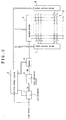
- Fig. 2 generally illustrates the configuration of a plasma display device which comprises a driver for driving a plasma display panel (hereinafter abbreviated as the "PDP") based on a driving method according to the present invention.
- PDP plasma display panel
- an A/D converter 1 samples an analog input video signal in response to a clock signal supplied thereto from a driving control circuit 2 to convert the same to 6-bit pixel data D (input pixel data) for each pixel, which is supplied to a data converting circuit 3.
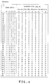
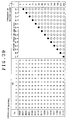
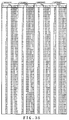
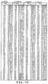
- the data converting circuit 3 converts the pixel data D to 9-bit converted pixel data HD (display pixel data) in accordance with a conversion table as shown in Figs. 3 and 4, and supplies the converted pixel data HD to a memory 4. It should be noted that the conversion table shown in Figs. 3 and 4 is merely an example of a conversion table for use in displaying a half-tone representation in 64 steps.
- the converted pixel data HD are sequentially written into the memory 4 in accordance with a write signal supplied thereto from the driving control circuit 2. Once the converted pixel data HD have been written into the memory 4 for one screen portion (n rows and m columns) through the writing operation, each of the converted pixel data HD 11-nm of the one screen portion is divided into respective bit digits (0th bit to 8th bit) which are read from the memory 4 and sequentially supplied to an address driver 6 for each row.
- data at the 0th bit in each of the m converted pixel data HD 11-1m corresponding to the first row of the screen is only read from the memory 4.
- data at the 0th bit in each of the converted pixel data HD 21-2m corresponding to the second row is only read from the memory 4.
- data at the 0th bit in the converted pixel data HD up to the nth row are only read sequentially from the memory 4 in a similar manner.
- data at the 1st bit in each of the m converted pixel data HD 11-1m corresponding to the second row on the screen is only read from the memory 4.
- the 9-bit converted pixel data HD converted in accordance with the conversion table as shown in Figs. 3 and 4 are divided into respective bit digits, and the divided data are sequentially read from the memory 4 from the 0th bit to the 8th bit and supplied to the address driver 6 within one field period.
- the address driver 6 generates pixel data pulses DP 1 - DP m each having a voltage corresponding to a logical level of a corresponding one in a group of pixel data bits for each row read from the memory 4, and applies these pixel data pulses PD 1 - DP m to column electrodes D 1 - D m , respectively.
- the driving control circuit 2 generates a clock signal to the A/D converter 1 and write and read signals to the memory 4 in synchronism with horizontal and vertical synchronization signals in an input video signal.
- the driving control circuit 2 also generates a pixel data timing signal, a reset timing signal, a scan timing signal and a sustain timing signal in synchronism with the horizontal and vertical synchronization signals.
- a first sustain driver 7 generates a resetting pulse RP x for initializing a residual charge amount, and a sustaining pulse IP x for sustaining a discharge light emitting state in response to a variety of timing signals supplied from the driving control circuit 2, and applies these pulses to row electrodes X 1 - X n of the PDP 10.
- a second sustain driver 8 generates a resetting pulse RP Y for initializing a residual charge amount, a scanning pulse SP for writing pixel data, a priming pulse PP for successfully performing the writing of pixel data, and a sustaining pulse IP Y for sustaining a discharge light emitting state in response to a variety of timing signals supplied from the driving control circuit 2, and applies these pulses to the row electrodes Y 1 - Y n of the PDP 10.
- a row electrode for one row of the screen is formed of a pair of a row electrode X and a row electrode Y.
- a row electrode pair for the first row in the PDP 10 is formed of row electrodes X 1 , Y 1
- a row electrode pair for the nth row is formed of row electrodes X n , Y n .
- a discharge cell is formed at an intersection of a row electrode pair with each of column electrodes.
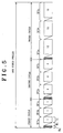
- Fig. 5 illustrates a light emission driving format within one field period which is relied on by the data converting circuit 3 when it uses a data conversion table as shown in Figs. 3 and 4.
- one field period is divided into nine subperiods.
- discharge light emission (first reset cycle) through subfields SF1a - SF1c is performed in first to third subperiods
- discharge light emission (second reset cycle) through subfields SF2a - SF2c is performed in fourth to sixth subperiods
- discharge light emission (third reset cycle) through subfields SF3a - SF3c is performed in seventh to ninth subperiods.
- a pixel data writing stage Wc for writing converted pixel data HD to set discharge cells to emitting cells or non-emitting cells, and a light emission sustaining stage Ic for sustaining a discharge light emitting state in the light emitting cells are included.
- only discharge cells set to emitting cells in the pixel data writing stage Wc are discharged to emit light in the light emission sustaining stage Ic.
- a light emitting time for discharge light emission performed in each subfield during the light emission sustaining stage Ic is as follows, assuming that a light emitting time in each of the subfields SF1a - SF1c is "1":
- the logical levels of the 0th - 8th bits of the converted pixel data HD determine light emission/non-light emission in each of the nine subfields SF1a - SF3c, as illustrated in Fig. 5.
- the 0th - 8th bits of the converted pixel data HD determine whether or not light should be emitted in the respective subfields in a correspondence relationship as shown below:
- Selective erasure discharge is executed only in a subfield corresponding to a logical level "1" in the converted pixel data HD. Therefore, a light emitting state is found in a subfield corresponding to a logical level "0" arranged before a subfield corresponding to a logical level "1,” and a non-light emitting state is found in a subfield corresponding to logical level "0" in each of the first to third reset cycles.
- converted pixel data HD [1,0,0,1,0,0,0,0,1] corresponding to a luminance level "32" as shown in Fig. 4, light is emitted by sustain discharge only in the subfield SF3a and the subfield SF3b within nine subfields in Fig. 5.
- a simultaneous resetting stage Rc in which reset discharge is excited in all discharge cells to form a wall charge in each of the discharge cells is executed only in the subfields SF1a, SF2a, SF3a which are the first subfields of the first to third reset cycles, as indicated by hatchings in Fig. 5.
- Figs. 6A to 6G are waveform charts showing application timings for a variety of driving pulses actually applied to associated electrodes of the PDP 10 in each of the subfields illustrated in Fig. 5. As can be seen, however, Figs. 6A to 6G only show such application timings in the first reset cycle extracted from the first to third reset cycles illustrated in Fig. 5.
- the first sustain driver 7 and the second sustain driver 8 first apply row resetting pulses RPx, PR Y simultaneously to electrodes X, Y of the PDP 10, respectively, to reset or discharge all discharge cells in the PDP 10 to forcedly form a wall charge in each of the discharge cells (simultaneous resetting stage Rc in Fig. 6G).
- the address driver 6 sequentially applies data pulses DP0 1 - DP0 m , corresponding to respective rows, to column electrodes D 1 - D m , as shown in Fig. 6B.
- each of the data pulses DP0 1 - DP0 m applied to the column electrodes D 1 - D m corresponds to the 0th bit in the converted pixel data HD as shown in Fig. 3.
- the second sustain driver 8 sequentially applies a scanning pulse SP to row electrodes Y 1 - Y n at the same timing as the application timing for each of the data pulses DP, as shown in Figs. 6D to 6F.
- discharge occurs only in a discharge cell at the intersection of a "row” applied with the scanning pulse SP with a "column” applied with a high-voltage pixel data pulse to selectively erase the wall charge remaining in the discharge cell.
- the selective erasure results in setting a light emitting discharge cell in which discharge light emission is performed in a sustain light emission stage and a non-light emitting discharge cell in which discharge light emission is not performed, as will be described later.
- a priming pulse PP of positive polarity is sequentially applied to the row electrodes Y 1 -Y n .
- Priming discharge excited in response to the application of the priming pulse PP permits restoration of charged particles in a discharge space of the PDP 10, which was formed in the simultaneous resetting stage Rc but has reduced over time. Therefore, pixel data is written by the application of the scanning pulse SP, while such charged particles still remain within the discharge space (pixel data writing stage Wc1 in Fig. 6G).
- the first sustain driver 7 and the second sustain driver 8 apply the sustaining pulses IP X , IP Y alternately to the row electrodes X, Y, as shown in Figs. 6C to 6F.
- a discharge cell which still holds the wall charge formed during the pixel data writing stage Wc1, i.e., a light emitting discharge cell repeats discharge light emission to sustain its light emitting state during a period in which it is applied alternately with the sustaining pulses IP X , IP Y (light emission sustaining stage Ic1 in Fig. 6G).
- the address driver 6 next applies data pulses DP1 1 - DP1 m corresponding to respective rows sequentially to the column electrodes D 1 - D m as shown in Fig. 6B.
- Each of the data pulses DP1 1 - DP1 m applied to the column electrodes D 1 - D m at this time corresponds to the 1st bit in the converted pixel data HD as shown in Fig. 3.
- the second sustain driver 8 sequentially applies the scanning pulse SP to the row electrodes Y 1 - Y n at the same timing as the timing at which the respective data pulses DP are applied, as shown in Figs. 6D - 6F.
- discharge occurs only in a discharge cell at the intersection of a "row” applied with the scanning pulse SP with a "column” applied with the high-voltage pixel data pulse to selectively erase a wall charge remaining in the discharge cell.
- the selective erasure results in a light emitting discharge cell in which discharge light emission can be performed in a light emission sustaining stage Ic2, later described, and a non-light emitting discharge cell in which discharge light emission is not performed.
- the priming pulse PP of positive polarity is sequentially applied to the row electrodes Y 1 - Y n .
- the application of the priming pulse PP permits restoration of charged particles in a discharge space of the PDP 10. Therefore, pixel data is written by the application of the scanning pulse SP, while such charged particles still remain within the discharge space (pixel data writing stage Wc2 in Fig. 6G).
- the first sustain driver 7 and the second sustain driver 8 apply the sustaining pulses IP X , IP Y alternately to the row electrodes X, Y, as shown in Figs. 6C to 6F.
- a discharge cell which still holds the wall charge formed during the pixel data writing stage Wc2, i.e., a light emitting discharge cell repeats discharge light emission to sustain its light emitting state during a period in which it is applied alternately with the sustaining pulses IP X , IP Y (light emission sustaining stage Ic2 in Fig. 6G).
- the address driver 6 next applies data pulses DP2 1 - DP2 m corresponding to respective rows sequentially to the column electrodes D 1 - D m as shown in Fig. 6B.
- Each of the data pulses DP2 1 - DP2 m applied to the column electrodes D 1 - D m at this time corresponds to the 2nd bit in the converted pixel data HD as shown in Fig. 3.
- the second sustain driver 8 sequentially applies the scanning pulse SP to the row electrodes Y 1 - Y n at the same timing as the timing at which the respective data pulses DP are applied, as shown in Figs. 6D - 6F.
- discharge occurs only in a discharge cell at the intersection of a "row” applied with the scanning pulse SP with a "column” applied with the high-voltage pixel data pulse to selectively erase a wall charge remaining in the discharge cell.
- the selective erasure results in a light emitting discharge cell in which discharge light emission can be performed in a light emission sustaining stage, later described, and a non-light emitting discharge cell in which discharge light emission is not performed.
- the priming pulse PP of positive polarity is sequentially applied to the row electrodes Y 1 - Y n .
- the application of the priming pulse PP permits restoration of charged particles in a discharge space of the PDP 10. Therefore, pixel data is written by the application of the scanning pulse SP, while such charged particles still remain within the discharge space (pixel data writing stage Wc3 in Fig. 6G).
- the priming discharge caused by the application of the priming pulse PP in the pixel data writing stages Wc2, Wc3 is only produced in light emitting discharge cells in which the discharge has been repeated to sustain light emission in the preceding light emission sustaining stages Ic1, Ic2, respectively.
- the first sustain driver 7 and the second sustain driver 8 applies the sustaining pulses IP X , IP Y alternately to the row electrodes X, Y.
- a discharge cell which still holds the wall charge formed during the pixel data writing stage Wc2, i.e., a light emitting discharge cell repeats discharge light emission to sustain its light emitting state during a period in which it is applied alternately with the sustaining pulses IP X , IP Y (light emission sustaining stage Ic3 in Fig. 6G).
- the simultaneous resetting operation is executed only three times, at the head of the first to third reset cycles during one field period. This can be accomplished because pixel data are converted in accordance with the tables of Figs. 3 and 4 so as to ensure that each of all discharge cells transitions from a light emitting discharge cell to a non-light emitting discharge cell once or less in one reset cycle as shown in Figs. 6A - 6G.
- the arrangement of the 0th - 2nd bits in the converted pixel data HD which govern whether or not light should be emitted in each of the subfields SF1a - SF1c (first reset cycle), are limited only to the following four patterns, as shown in Figs. 3 and 4:
- the present invention prohibits such a data pattern that returns a discharge cell, which has once been set to a light emitting discharge cell in a single reset cycle, again to a non-light emitting discharge cell.
- the contrast can be enhanced as compared with the prior art format which requires the simultaneous resetting operation six times during one field period, as illustrated in Fig. 1.
- the selective erasing discharge (transition from a light emitting discharge cell to a non-light emitting discharge cell) is performed at maximum only once in each of the first - third reset cycles illustrated in Fig. 5, so that the number of times the selective erasing discharge is executed in one field period is merely three times at maximum.
- a subfield having a long light emitting period is divided into a plurality of subfields in such a manner as to ensure that at least one of these divided subfields is brought into a light emitting state when a display is produced at a predetermined luminance level or more.
- a display is produced at a predetermined luminance level or more.
- associated pixel data is converted such that the subfield SF3a, which has the longest light emitting period within the subfields SF3a - SF3c in Fig. 5, is brought into a light emitting state.
- the PDP 10 is driven using a conversion table as shown in Figs. 3 and 4 for the data conversion circuit 3 and in accordance with the light emission driving format as illustrated in Fig. 5, the present invention is not limited to this particular configuration.
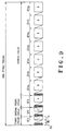
- one field period is partitioned into first to tenth subperiods, wherein discharge light emission through a subfield SF1 is performed in a first subperiod (first reset cycle); discharge light emission through a subfield SF2 in a second subperiod (second reset cycle); discharge light emission through a subfield SF3 in a third subperiod (third reset cycle); and discharge light emission through a subfield SF4 in fourth to tenth subperiods SF4a - SF4g (fourth reset cycle).
- a light emitting time for discharge light emission performed in each of the subfields SF1 - SF4 is as follows, assuming that a light emitting time in the subfield SF1 is "1":
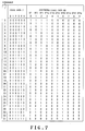
- the logical levels of the 0th - 9th bits of the converted pixel data HD as shown in Figs. 7 and 8 determine whether or not light should be emitted in each of the subfields SF1, SF2, SF3, SF4a - SF4g, as illustrated in Fig. 9.
- the 0th - 9th bits of the converted pixel data HD determine whether or not light should be emitted in the respective subfields in a correspondence relationship as shown below:
- a simultaneous resetting stage Rc as indicated by hatching is performed only at the head of each reset cycle.
- data is converted on the basis of Figs. 7 and 8 so as to ensure that each of all discharge cells transitions from a light emitting discharge cell to a non-light emitting discharge cell once or less.
- the arrangement of the 3rd - 9th bits in converted pixel data HD governing whether or not light should be emitted in each of the subfields SF4a - SF4g is limited only to the following eight patterns, as shown in Figs. 7 and 8:
- the present invention prohibits such a data pattern that returns a discharge cell, which has once been set to a light emitting discharge cell, again to a non-light emitting discharge cell in the fourth reset cycle.
- the contrast can be enhanced as compared with the prior art format, as illustrated in Fig. 1, which requires the simultaneous resetting operation six times during one field period.
- the selective erasing discharge (transition from a light emitting discharge cell to a non-light emitting discharge cell) is performed at maximum only once in each of the first - fourth reset cycles as illustrated in Fig. 9, so that the total number of times the selective erasing discharge is executed in one field period is merely four at maximum.
- converted pixel data HD corresponding to the luminance level "7" is:
- bits corresponding to the subfields SF1, SF2, SF3, SF4a in the light emission pattern are all inverted, so that this can be viewed as an erroneous contour.
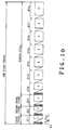
- Fig. 10 illustrates a light emission driving format according to another embodiment which is created in view of the occurrence of such a pseudo-contour
- Figs. 11 and 12 shows a conversion table for use in driving the PDP in accordance with this light emission driving format.
- the light emission period ratio "8" in the subfield SF4a shown in Fig. 9 is reduced to "4" which is identical to that of the subfield SF3 positioned preceding thereto, and the reduced portion is compensated for by increasing the light emission period ratio of the subfield SF4g to "12."
- converted pixel data HD corresponding to the luminance level "7" can be set to:
- a duration of sustained light emission, performed in the first subfield SF4a in a group of a plurality of subfields (fourth cycle), is first set identical to a duration of sustained light emission performed in the subfield SF3 preceding to the group of subfields.
- pixel data is converted as shown in Figs. 11 and 12 so as to ensure that either the first subfield SF4a in the group of subfields or the subfield SF3 maintains a light emitting state before the transition. More specifically, as shown in Fig. 11 and 12, when the luminance level changes one step, the bits corresponding to the subfields SF4a, SF3 in the light emission pattern are changed:
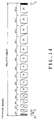
- Figs. 14 and 15 illustrate a light emission driving format for writing pixel data in accordance with the selective erasure address method as mentioned above in the pixel data writing stage Wc
- Fig. 15 illustrates a light emission driving format for writing pixel data in accordance with the selective writing address method.
- each of the subfields SF1 - SF14 includes a pixel data writing stage Wc for writing pixel data to set light emitting cells and non-light emitting cells, and a light emission sustaining stage Ic for sustaining a discharge light emitting state only in the light emitting cells.
- a light emitting time (the number of times of light emission) in each light emission sustaining stage Ic of the subfields SF1 - SF14 is set as follows, assuming that a light emitting time in the subfield SF1 is "1":
- the simultaneous resetting stage Rc is executed only in the first subfield. Specifically, the simultaneous resetting stage Rc is executed only in the subfield SF1 in the light emission driving format when employing the selective erasure address method as illustrated in Fig. 14, and only in the subfield SF14 in the light emission driving format when employing the selective writing method as illustrated in Fig. 15. In addition, an erasing stage E for extinguishing wall charges remaining in all discharge cells is executed in the last subfield of one field period, as illustrated in Figs. 14 and 15.
- Fig. 16 illustrates the configuration of a plasma display device for performing the light emission driving operations based on the light emission driving formats of Figs. 14 and 15.
- the plasma display device illustrated in Fig. 16 has a data converting circuit 30 instead of the data converting circuit 3 in the configuration illustrated in Fig. 2, and the rest of functional modules except for the data converting circuit 30 are identical to those illustrated in Fig. 2. Therefore, the following description will be made only on the operation of the data converting circuit 30 illustrated in Fig. 16.
- Fig. 17 is a block diagram illustrating the internal configuration of the data converting circuit 30.
- an ABL (automatic brightness limiting) circuit 31 adjusts the luminance level of pixel data D for each pixel sequentially supplied thereto from an A/D converter 1 such that an average luminance of pixels displayed on the screen of the PDP 10 falls within a predetermined luminance range, and supplies the resulting luminance adjusted pixel data D BL to a first data converting circuit 32.
- the ABL circuit 31 is adapted to conduct an inverse gamma correction on the pixel data D (input pixel data), and automatically adjust the luminance level of the pixel data D (input pixel data) in accordance with an average luminance of the thus produced inverse gamma converted pixel data. This can prevent the display quality from degrading due to the luminance adjustment.
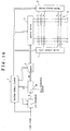
- Fig. 18 is a block diagram illustrating the internal configuration of the ABL circuit 31.
- a level adjusting circuit 310 adjusts the level of pixel data D in accordance with an average luminance calculated in an average luminance detecting circuit 311, later described, and outputs resulting luminance adjusted pixel data D BL .
- the data converting circuit 312 conducts the inverse gamma correction on the luminance adjusted pixel data D BL to recover pixel data (inverse gamma converted pixel data Dr) corresponding to an original video signal from which the gamma correction has been removed.
- the average luminance detecting circuit 311 calculates an average luminance from the inverse gamma converted pixel data Dr, and supplies the average luminance to the level adjusting circuit 310.
- the average luminance detecting circuit 311 also selects a luminance mode available for driving the PDP 10 to emit light at a luminance in accordance with the average luminance calculated as mentioned above, from luminance modes 1 - 4 which specify light emitting times in the respective subfields, for example, as shown in Fig. 20, and supplies a luminance mode signal LC indicative of the selected luminance mode to a driving control circuit 2.
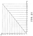
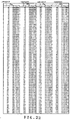
- the first data converting circuit 32 converts input luminance adjusted pixel data D BL capable of representing 256 steps of gradation (8 bits) to 8-bit (0 - 244) converted pixel data HD P having the number of gradation levels reduced by 14 ⁇ 16/255 (224/255), based on a conversion characteristic as shown in Fig. 21, and supplies the converted pixel data HD P to a multi-level gradation conversion processing circuit 33.
- the 8-bit input luminance adjusted pixel data D BL (0 - 255) is converted in accordance with a conversion table as shown in Figs. 22 and 23 based on the conversion characteristic as mentioned.
- the conversion characteristic is determined in accordance with the number of bits of input pixel data, the number of compressed bits by multi-level gradation conversion, and the number of steps of gradation in display.
- the first data converting circuit 32 is disposed in front of the multi-level gradation conversion processing circuit 33, later described, to perform a conversion in accordance with the number of steps in gradation and the number of compressed bits by multi-tone, to thereby divide the luminance adjusted pixel data D BL into a group of upper bits (corresponding to multi-tone pixel data) and a group of lower bits (data to be truncated, i.e., error data) on a bit boundary, and to perform multi-level gradation conversion processing based on the multi-tone pixel data.
- This can prevent the occurrence of luminance saturation due to the multi-level gradation conversion processing, and the occurrence of flatness in the display characteristic which may be found when display gradation does not lie on the bit boundary (i.e., occurrence of gradation distortion).
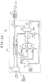
- Fig. 24 is a block diagram illustrating the internal configuration of the multi-level gradation conversion processing circuit 33. As illustrated in Fig. 24, the multi-level gradation conversion processing circuit 33 is composed of an error diffusion processing circuit 330 and a dither processing circuit 350.
- a data separating circuit 331 in the error diffusion processing circuit 330 separates m-bit converted pixel data HD P supplied from the first data converting circuit 32 illustrated in Fig. 17 into lower i bits as error data and upper (m-i) bits as display data.
- An adder 332 adds the lower i bits of the converted pixel data HD P as the error data, a delay output from a delay circuit 334, and a multiplication output of a coefficient multiplier 335 to produce an addition value which is supplied to a delay circuit 336.
- the delay circuit 336 delays the addition value supplied from the adder 332 by a delay time D having the same time as a clock period of the pixel data to produce a delayed addition signal AD 1 which is supplied to the coefficient multiplying circuit 335 and to a delay circuit 337, respectively.
- the coefficient multiplier 335 multiplies the delayed addition signal AD 1 by a predetermined coefficient value K 1 (for example, "7/16"), and supplies the multiplication result to the adder 332.
- the delay circuit 337 again delays the delayed addition signal AD 1 by a time equal to (one horizontal scan period minus the delay time D multiplied by four) to produce a delayed addition signal AD 2 which is supplied to a delay circuit 338.
- the delay circuit 338 further delays the delayed addition signal AD 2 by the delay time D to produce a delayed addition signal AD 3 which is supplied to a coefficient multiplier 339.
- the delay circuit 338 further delays the delayed addition signal AD 2 by a time equal to the delay time D multiplied by two to produce a delayed addition signal AD 4 which is supplied to a coefficient multiplier 340.
- the delay circuit 338 further delays the delayed addition signal AD 2 by a time equal to the delay time D multiplied by three to produce a delayed addition signal AD 5 which is supplied to a coefficient multiplier 341.
- the coefficient multiplier 339 multiplies the delayed addition signal AD 3 by a predetermined coefficient value K 2 (for example, "3/16"), and supplies the multiplication result to an adder 342.
- the coefficient multiplier 340 multiplies the delayed addition signal AD 4 by a predetermined coefficient value K 3 (for example, "5/16"), and supplies the multiplication result to the adder 342.
- the coefficient multiplier 341 multiplies the delayed addition signal AD 5 by a predetermined coefficient value K 4 (for example, "1/16"), and supplies the multiplication result to the adder 342.
- the adder 342 adds the multiplication results supplied from the respective coefficient multipliers 339, 340, 341 to produce an addition signal which is supplied to the delay circuit 334.
- the delay circuit 334 delays the addition signal by the delay time D to produce a delayed signal which is supplied to the adder 332.
- the adder 332 adds the lower i bits of the converted pixel data HD P , the delayed signal output from the delay circuit 334 and the multiplication output from the coefficient multiplier 335, and generates a carry-out signal C O which is at logical level "0" when a carry is not generated as a result of the addition, and at logical level "1" when a carry is generated.
- the carry-out signal C O is supplied to an adder 333.
- the adder 333 adds the carry-out signal C O to display data consisting of the upper (m-i) bits of the converted pixel data HD P to output the error diffusion processed pixel data ED having (m-i) bits. Consequently, the number of bits of the error diffusion processed pixel data ED is smaller than that of the converted pixel data HD P .
- pixel data ED For producing error diffusion processed pixel data ED corresponding to a pixel G(j, k) for the PDP 10, for example, as illustrated in Fig. 25, respective error data corresponding to a pixel G(j, k-1) on the left side of the pixel G(j, k), a pixel G(j-1, k-1) off to the upper left of the pixel G(j, k), a pixel G(j-1, k) above the pixel G(j, k), and a pixel G(j-1, k+1) off to the upper right of the pixel G(j, k), i.e.:
- the error diffusion processing circuit 330 regards the upper (m-i) bits of the converted pixel data HD P as display data, and the remaining lower i bits as error data, and reflects the weighted addition of the error data at the respective peripheral pixels ⁇ G(j, k-1), G(j-1, k+1), G(j-1, k), G(j-1, k-1) ⁇ to the display data.
- the luminance for the lower i bits of the original pixel ⁇ G(j, k) ⁇ is virtually represented by the peripheral pixels, so that gradation representation of luminance equivalent to that provided by the m-bit pixel data can be accomplished with display data having a number of bits less than m bits, i.e., (m-i) bits.
- the coefficients K 1 -K 4 for the error diffusion to be assigned to four pixels may be changed from field to field in a manner similar to dither coefficients, later described.
- the dither processing circuit 350 performs dither processing on the (m-i)-bit error diffusion processed pixel data ED supplied from the error diffusion processing circuit 330 to generate multi-level gradation converted pixel data D S which has the number of bits reduced to (m-i-j) bits while maintaining the number of levels of luminance gradation equivalent to the error diffusion processed pixel data ED.
- the dither processing refers to representation of an intermediate display level with a plurality of adjacent pixels.
- a gradation display comparable to 8 bits using upper 6 bits of 8-bit pixel data For example, for achieving a gradation display comparable to 8 bits using upper 6 bits of 8-bit pixel data, four pixels vertically and horizontally adjacent to each other are grouped into a set, and four dither coefficients a - d having coefficient values different from each other are assigned to respective pixel data corresponding to the respective pixels in the set, and added.
- a combination of four different intermediate display levels can be produced with four pixels.
- an available number of levels of luminance gradation are four times as much. In other words, a half tone display comparable to that provided by 8 bits can be achieved.
- the dither processing circuit 350 changes the dither coefficients a - d assigned to four pixels from field to field.
- Fig. 26 is a block diagram illustrating the internal configuration of the dither processing circuit 350.
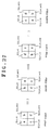
- a dither coefficient generating circuit 352 generates four dither coefficients a , b , c , d for four mutually adjacent pixels, and supplies these dither coefficients sequentially to an adder 351. For example, as shown in Fig.
- four dither coefficients a , b , c , d are generated corresponding to four pixels: a pixel G(j, k) and a pixel G(j, k+1) corresponding to a jth row, and a pixel (j+1, k) and a pixel G(j+1, k+1) corresponding to a (j+1)th row, respectively.
- the dither coefficient generating circuit 352 changes the dither coefficients a - d assigned to these four pixels from field to field as shown in Fig. 27.
- the dither coefficients a - d are repeatedly generated in a cyclic manner with the following assignment:
- the adder 351 adds the dither coefficients a - d assigned to each of the fields as described above to each of the error diffusion processed pixel data ED, supplied thereto from the error diffusion processing circuit 330, corresponding to the pixels G(j, k), G(j, k+1), G(j+1, k), G(j+1, k+1) to produce dither added pixel data which is supplied to an upper bit extracting circuit 353.
- the adder 351 sequentially supplies:
- the upper bit extracting circuit 353 extracts upper (m-i-j) bits of the dither added pixel data, and supplies the extracted bits to the second data converting circuit 34 illustrated in Fig. 17 as multi-level gradation converted pixel data D S .
- the second data converting circuit 34 converts the multi-level gradation converted pixel data D S to converted pixel data HD (display pixel data) consisting of 1st to 14th bits corresponding to the subfields SF1 - SF14, respectively, illustrated in Fig. 14 or 15 in accordance with a conversion table shown in Fig. 28 or Fig. 29.
- the multi-level gradation converted pixel data D S is produced by reducing the number of possible gradation levels of 8-bit input pixel data D (256 gradation levels) in a ratio of 224/225 in accordance with a first data conversion (the conversion table in Figs. 22 and 23), and converting the reduced data to 4-bit data (0 - 14: 15 gradation levels) by multi-level gradation conversion processing (for example, a total of four bits are compressed, two bits in the error diffusion processing and two bits in the dither processing).
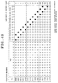
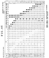
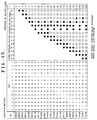
- Fig. 28 shows a conversion table for use in light emission driving in accordance with the selective erasure address method as illustrated in Fig. 14, and Fig. 29 shows a conversion table for use in light emission driving in accordance with the selective writing method as illustrated in Fig. 15.
- a bit at logical level "1" in converted pixel data HD consisting of 1st - 14th bits indicates that selective erasure discharge (selective write discharge) is performed in a pixel data writing stage Wc in a subfield SF corresponding to the bit.
- the converted pixel data HD are sequentially written into the memory 4 illustrated in Fig. 16 in response to a write signal supplied thereto from the driving control circuit 2.
- the one screen portion of converted pixel data HD 11-nm is divided into the respective bit digits (1st - 14th bits). The divided bits are read from the memory 4 and supplied sequentially to the address driver 6 for each row.
- the 14-bit converted pixel data HD which have been converted in accordance with the conversion table as shown in Fig. 28, are divided into the respective bit digits, and sequentially read from the memory 4 from the 1st bit to the 14th bit and supplied to the address driver 6 in one field period.
- the address driver 6 generates pixel data pulses DP 1 -DP m each having a voltage corresponding to a logical level of a corresponding one in a group of pixel data bits for each row, read from the memory 4, and an erasing pulse AP for erasing a remaining charge, and applies these pulses to column electrodes D 1 - D m of the PDP 10 at the timings as illustrated in Figs. 30A through 30G or Figs. 31A through 31G.
- the driving control circuit 2 generates a clock signal to the A/D converter 1 and write and read signals to the memory 4 in synchronism with horizontal and vertical synchronization signals in an input video signal.
- the driving control circuit 2 also generates a pixel data timing signal, a reset timing signal, a scan timing signal and a sustain timing signal in synchronism with the horizontal and vertical synchronization signals.
- the driving control circuit 2 sets the number of times (or a period in which) the sustain timing signal is supplied in each light emission sustaining stage Ic illustrated in Fig. 14 or 15, i.e., the number of the sustain timing pulses supplied in each light emission sustaining stage Ic illustrated in Fig.
- the number of sustain timing pulses is set to "1" when a mode 1 is specified by the luminance mode signal LC; to "2" when a mode 2 is specified; to "3" when a mode 3 is specified; and to "4" when a mode 4 is specified.
- a first sustain driver 7 generates a resetting pulse RP x for initializing a residual charge amount, and a sustaining pulse IP x for sustaining a discharge light emitting state in response to a variety of timing signals supplied from the driving control circuit 2, and applies these pulses to row electrodes X 1 - X n of the PDP 10 at timings as illustrated in Figs. 30C or 31C.
- a second sustain driver 8 generates a resetting pulse RP Y for initializing a residual charge amount, a scanning pulse SP for writing pixel data, a priming pulse PP for successfully performing the writing of pixel data, a sustaining pulse IP Y for sustaining a discharge light emitting state, and an erasing pulse EP for erasing remaining wall charge in response to a variety of timing signals supplied from the driving control circuit 2, and applies these pulses to row electrodes Y 1 - Y n of the PDP 10 at timings as illustrated in Figs. 30D to 30F or in Figs. 31D to 31F.
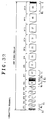
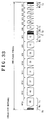
- Figs. 30A - 30G illustrate application timings for a variety of driving pulses in one field period during the light emission driving in accordance with the selective erasure address method
- Figs. 31A - 31G illustrate application timings for a variety of driving pulses in one field period during the light emission driving in accordance with the selective writing address method.
- the first sustain driver 7 and the second sustain driver 8 first apply the resetting pulses RP X , RP Y , respectively to row electrodes X, Y of the PDP 10 to reset or discharge all discharge cells in the PDP 10 to forcedly form a wall discharge in each of the discharge cells (R 1 in Fig. 31G).
- the first sustain driver 7 simultaneously applies the erasing pulse EP to the row electrodes X 1 - X n of the PDP 10 to erase the wall charges formed in all the discharge cells (R 2 in Fig. 31G).
- a sequence of operations R 1 , R 2 implements the simultaneous resetting stage Rc. In a pixel data writing stage Wc in Figs.
- discharge occurs only in a discharge cell at the intersection of a "row” applied with the scanning pulse SP with a "column” applied with a high-voltage pixel data pulse to selectively erase the wall charge remaining in the discharge cell.
- Such selective erasure results in setting a light emitting discharge cell in which discharge light emission is performed in a light emission sustaining stage Ic and a non-light emitting discharge cell in which discharge light emission is not performed.
- erasing discharge is selectively performed only in a subfield SF corresponding to a bit at logical level "1" in converted pixel data HD (indicated by a black circle), as shown in Fig. 28.
- a lighting state is sustained in subfields SF which exist between the first subfield SF1 and the subfield in which the selective erasing discharge is performed (indicated by white circles).
- an extinct state is sustained.
- actual luminance of emitted light may change depending on a mode specified by the luminance mode signal LC as shown in Fig. 20. Specifically, a light emission period in each of the light emission sustaining stages Ic illustrated in Figs. 14 and 15 is defined for the mode 1 in Fig. 20. Otherwise, luminance twice as much as that of the mode 1 is represented when the mode 2 is specified by the luminance mode signal LC; three times when the mode 3 is specified; and four times when the mode 4 is specified.
- the driving method illustrated in Figs. 14 and Figs. 31A - 31G is such that the simultaneous resetting stage Rc is executed only at the subfield located at the head of one field period while desired luminance is maintained, and the respective discharge pixels are set to either a light emitting cell or a non-light emitting cell in accordance with pixel data only in a pixel data writing stage of any one of subfields.
- the luminance may be increased by bringing the subfields in one field into a lighting state in order from the first subfield when the selective erasure address method is employed, or by bringing the subfields in one field into a lighting state in order from the last subfield when the selective writing address method is employed.
- Figs. 32 and 33 illustrate other light emission driving formats for driving light emission with the configuration illustrated in Figs. 16 - 18.
- subfields in one field is divided into two groups of subfields each including a plurality of subfields arranged consecutively to each other, wherein a simultaneous resetting stage Rc is executed only in a subfield arranged at the head of each subfield group, and each of discharge cell is bet to either a light emitting cell or a non-light emitting cell in accordance with pixel data only in a pixel data writing stage in any one of the subfields.
- the simultaneous resetting operation and the selective erasing operation selective writing operation
- the luminance may be increased by bringing the subfields in one field into a lighting state in order from the first subfield when the selective erasure address method is employed, or by bringing the subfields in one field into a lighting state in order from the last subfield when the selective writing address method is employed.
- Fig. 32 illustrates a light emission driving format for writing pixel data in accordance with the selective erasure address method as mentioned above in the pixel data writing stage Wc
- Fig. 33 illustrates a light emission driving format for writing pixel data in accordance with the selective writing address method.
- each of the subfields SF1 - SF14 includes a pixel data writing stage Wc for writing pixel data to set discharge cells to light emitting cells or non-light emitting cells, and a light emission sustaining stage Ic for sustaining a discharge light emitting state only in the light emitting cells.
- a light emitting time (the number of times of light emission) in each light emission sustaining stage Ic of the subfields SF1 - SF14 is as follows, assuming that a light emitting time in the subfield SF1 is "1":
- the simultaneous resetting stage Rc is executed in the first subfield and an intermediate subfield in these subfields. Specifically, the simultaneous resetting stage Rc is executed in the subfields SF1, SF7 in the light emission driving format when employing the selective erasure address method as illustrated in Fig. 32, and in the subfield SF14, SF6 in the light emission driving format when employing the selective writing method as illustrated in Fig. 33.
- an erasing stage E for extinguishing wall charges remaining in all discharge cells is executed in the last subfield of one field period and in subfields immediately before the subfields in which the simultaneous resetting stage Rc is executed, as illustrated in Figs. 32 and 33.
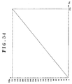
- Fig. 34 illustrates a conversion characteristic of the first data converting circuit 32 in Fig. 17 which is applied when the light emission driving is performed on the basis of the light emission driving formats illustrated in Figs. 32 and 33.
- Figs. 35 and 36 show an example of a conversion table based on the conversion characteristic of Fig. 34.
- the first data converting circuit 32 converts input luminance adjusted pixel data D BL capable of representing 256 steps of gradation (8 bits) to 9-bit (0 - 352) converted pixel data HD P having the number of gradation levels increased by 22 ⁇ 16/255 (352/255), based on a conversion table of Figs. 35 and 36, and supplies the converted pixel data HD P to the multi-level gradation conversion processing circuit 33.
- the multi-level gradation conversion processing circuit 33 performs, for example, 4-bit compress processing similar to the foregoing to output 5-bit multi-level gradation converted pixel data D S (0 - 22).
- Figs. 37 and 38 each show a conversion table for use in the second data converting circuit 34 illustrated in Fig. 17, and a driving state in one field.
- Fig. 37 shows a conversion table used when light emission is driven in accordance with the selective erasure address method as illustrated in Fig. 32
- Fig. 38 shows a conversion table used when light emission is driven in accordance with the selective writing method as illustrated in Fig. 33.
- multi-level gradation converted pixel data D S is produced by increasing the number of possible gradation levels of the 8-bit input pixel data D (256 gradation levels) in a ratio of 352/225 in accordance with a first data conversion (the conversion table in Figs. 22 and 23), and converting the increased data to 5-bit data (0 - 22: 23 gradation levels) by multi-level gradation conversion processing (for example, a total of four bits are compressed, two bits in the error diffusion processing and two bits in the dither processing).
- the selective erasing (write) discharge is generated in the pixel data writing stage Wc by simultaneously applying the scanning pulse SP and the pixel data pulse of a high voltage.
- the selective erasing (write) discharge is not generated normally even if the scanning pulse SP and the pixel data pulse of a high voltage are applied simultaneously, so that the wall charge in the discharge cell is not erased or formed.
- a light emission corresponding to the highest luminance level will be effected even if the pixel data D after the A/D conversion represents a low luminance level. This will greatly degrade the quality of the image.
- the selective erasure address scheme is adopted as the pixel data writing method
- the converted pixel data HD is [0,1,0,0,0,0,0,0,0,0,0,0,0,0,0,0,0]
- the selective erasing discharge is performed only in the subfield SF2 as indicated by the black dots in Fig. 28.
- the discharge cells are changed to the non-light emitting cell.
- the sustain light emission should be effected only in the subfield SF1 among the subfields SF1 through SF14.
- the sustain light emission is performed not only in the subfield SF1 but also in the subfields SF1 through SF14 following it. This will result in a display at the highest luminance level.
- the light emission driving patterns shown in Figs. 39 through 45 are adopted to prevent such an erroneous light emitting operation.
- Figs. 39 through 45 show light emission driving patterns for preventing the erroneous light emitting operations, and examples of the conversion table used in the second data converting circuit 34 when effecting such light emission driving operations.
- Figs. 39 through 43 all patterns of the light emitting driving effected based on the light emission driving format shown in Fig. 14 or Fig. 15 in which the simultaneous resetting stage Rc is provided only once in one field period, and examples of the conversion table used in the second data converting circuit 34 when effecting these light emission driving operations.
- Figs. 39 through 41 show the formats of the light emission driving when the selective erasure address scheme shown in Fig. 14 is adopted
- Figs. 42 and 43 show the patterns of light emission driving effected based on the light emission driving format when the selective writing addres scheme shown in Fig. 15 is adopted.
- the selective erasing (write) discharge is consecutively performed in the pixel data writing stage Wc in each of the consecutive two subfields, as shown by the black dots in the figure.
- the elimination or the formation of the wall charge is normally performed by the second selective erasing (write) discharge even if the wall charge in the discharge cell is not normally eliminated or formed in the first selective erasing (write) discharge, so that the erroneous sustain light emission mentioned above is surely prevented.
- Fig. 40 shows a light emitting drive pattern performed in view of the point described above, and an example of the conversion table of the second data converting circuit 34.
- the second selective erasing (write) discharge is performed after the lapse of one subfield subsequent to the execution of the first selective erasing (write) discharge.
- the number of times of the selective erasure (writin) discharge to be performed in one field period is not limited to twice.
- Figs. 41 and 43 show a pattern of the light emitting driving and an example of the conversion table of the second data converting circuit 34 adopted in view of the point described above.
- the sign "*" shown in Figs. 41 and 43 represents that it may take either one of logical values "1" and “0", and the triangle indicates that the selective erasing (write) discharge is performed only when the sign "*" has the logical level "1".
- the selective erasing (write) discharge is performed once more in one of the subfields existing thereafter, so as to ensure the writing of the pixel data.
- the display period of one field is divided to N (N is a natural number) subfields, and a subfield group of consecutive M (2 ⁇ M ⁇ N) subfields is formed.
- N is a natural number
- a discharge to initialize all of the discharge cell to one of the state of the light emitting cell and the state of the non-light emitting cell is produced only in the subfield in the head part of the subfield group.
- the writing of the pixel data is performed by applying, in one of the subfields in the the subfield group, first data pulse which generates a discharge to set each discharge cell to one of the non-light emitting cell and the light emitting cell.
- each subfield only the light emitting cells are driven to emmit light for a light emission period corresponding to the weight of the subfield.
- the writing of the pixel data is ensured by the application of a second pixel data pulse which is the same as the first pixel data pulse in one of the subfields exsisting after the application of the first pixel data pulse.
- the present invention can reduce the number of times the simultaneous resetting operation is performed for initializing all discharge cells in one field, the resulting image can be enhanced in contrast. Further, since the present invention can reduce the number of times the selective erasing (write) discharge is performed in each pixel data writing stage within one field period, a reduction in power consumption is achieved. Furthermore, since the present invention can prevent adjacent discharge cells in a light emission pattern from inverting with respect to each other even when a display includes a small amount of changes in luminance levels, the pseudo-contour can be suppressed.
Landscapes
- Engineering & Computer Science (AREA)
- Physics & Mathematics (AREA)
- Computer Hardware Design (AREA)
- General Physics & Mathematics (AREA)
- Theoretical Computer Science (AREA)
- Power Engineering (AREA)
- Plasma & Fusion (AREA)
- Control Of Indicators Other Than Cathode Ray Tubes (AREA)
- Control Of Gas Discharge Display Tubes (AREA)
Applications Claiming Priority (10)
| Application Number | Priority Date | Filing Date | Title |
|---|---|---|---|
| JP11224498 | 1998-04-22 | ||
| JP11224498 | 1998-04-22 | ||
| JP34452698 | 1998-12-03 | ||
| JP34452698 | 1998-12-03 | ||
| JP34895898 | 1998-12-08 | ||
| JP34895898 | 1998-12-08 | ||
| JP5623599 | 1999-03-03 | ||
| JP5623599A JP3789052B2 (ja) | 1998-12-03 | 1999-03-03 | プラズマディスプレイパネルの駆動方法 |
| JP06667899A JP3618571B2 (ja) | 1998-12-08 | 1999-03-12 | プラズマディスプレイパネルの駆動方法 |
| JP06667899 | 1999-03-12 |
Publications (2)
| Publication Number | Publication Date |
|---|---|
| EP0952569A2 true EP0952569A2 (fr) | 1999-10-27 |
| EP0952569A3 EP0952569A3 (fr) | 2000-09-13 |
Family
ID=27523286
Family Applications (1)
| Application Number | Title | Priority Date | Filing Date |
|---|---|---|---|
| EP99107909A Withdrawn EP0952569A3 (fr) | 1998-04-22 | 1999-04-21 | Méthode de commande d'un panneau d'affichage à plasma |
Country Status (3)
| Country | Link |
|---|---|
| US (1) | US6614413B2 (fr) |
| EP (1) | EP0952569A3 (fr) |
| CN (2) | CN100343886C (fr) |
Cited By (15)
| Publication number | Priority date | Publication date | Assignee | Title |
|---|---|---|---|---|
| EP1022714A2 (fr) * | 1999-01-18 | 2000-07-26 | Pioneer Corporation | Méthode de commande pour un panneau d'affichage à plasma |
| WO2001029812A1 (fr) | 1999-10-19 | 2001-04-26 | Matsushita Electric Industrial Co., Ltd. | Procede d'affichage par gradation permettant de reduire efficacement les papillotements et afficheur a gradation |
| WO2001045398A1 (fr) * | 1999-12-17 | 2001-06-21 | Koninklijke Philips Electronics N.V. | Procede et unite destines a afficher une image dans des sous-champs |
| WO2002005253A1 (fr) | 2000-07-07 | 2002-01-17 | Matsushita Electric Industrial Co., Ltd. | Procede et dispositif d'affichage |
| EP1265214A1 (fr) * | 2001-06-07 | 2002-12-11 | Pioneer Corporation | Panneau d'affichage à plasma et son procédé de commande |
| KR100373528B1 (ko) * | 2001-01-18 | 2003-02-25 | 엘지전자 주식회사 | 플라즈마 디스플레이 패널의 고속 구동방법 |
| KR100378622B1 (ko) * | 2001-02-09 | 2003-04-03 | 엘지전자 주식회사 | 선택적 쓰기 및 소거를 이용한 플라즈마 디스플레이패널의 구동방법 및 장치 |
| WO2003032352A3 (fr) * | 2001-10-03 | 2003-11-20 | Matsushita Electric Industrial Co Ltd | Procede et dispositif de commande d'ecran a plasma, et dispositif a ecran a plasma |
| US6674446B2 (en) * | 1999-12-17 | 2004-01-06 | Koninilijke Philips Electronics N.V. | Method of and unit for displaying an image in sub-fields |
| WO2002097777A3 (fr) * | 2001-05-29 | 2004-01-15 | Koninkl Philips Electronics Nv | Unite de commande d'affichage, procede d'affichage de pixels et appareil d'affichage comprenant ladite unite de commande |
| EP1124216A3 (fr) * | 2000-02-10 | 2005-10-05 | Pioneer Corporation | Méthode de commande d'un panneau d'affichage |
| DE20122842U1 (de) | 2001-05-08 | 2008-07-17 | Deutsche Thomson Ohg | Einrichtung zum Verarbeiten von Videobildern |
| US7466325B2 (en) | 2004-05-18 | 2008-12-16 | Semiconductor Energy Laboratory Co., Ltd. | Semiconductor display device and driving method |
| US7773161B2 (en) * | 2000-11-30 | 2010-08-10 | Thomson Licensing | Method and apparatus for controlling a display device |
| US7817170B2 (en) | 2004-08-03 | 2010-10-19 | Semiconductor Energy Laboratory Co., Ltd. | Display device and method for driving the same |
Families Citing this family (61)
| Publication number | Priority date | Publication date | Assignee | Title |
|---|---|---|---|---|
| JP3424587B2 (ja) * | 1998-06-18 | 2003-07-07 | 富士通株式会社 | プラズマディスプレイパネルの駆動方法 |
| JP3762568B2 (ja) | 1998-08-18 | 2006-04-05 | 日本碍子株式会社 | ディスプレイの駆動装置及びディスプレイの駆動方法 |
| US6791515B2 (en) * | 2000-08-23 | 2004-09-14 | Matsushita Electric Industrial Co., Ltd. | Image display apparatus for writing display information with reduced electric consumption |
| JP2004516513A (ja) * | 2000-12-20 | 2004-06-03 | コーニンクレッカ フィリップス エレクトロニクス エヌ ヴィ | マトリックス表示装置および方法 |
| US6791516B2 (en) * | 2001-01-18 | 2004-09-14 | Lg Electronics Inc. | Method and apparatus for providing a gray level in a plasma display panel |
| JP4066662B2 (ja) * | 2001-03-09 | 2008-03-26 | セイコーエプソン株式会社 | 電気光学素子の駆動方法、駆動装置及び電子機器 |
| US7091935B2 (en) * | 2001-03-26 | 2006-08-15 | Lg Electronics Inc. | Method of driving plasma display panel using selective inversion address method |
| KR20040010768A (ko) * | 2001-06-20 | 2004-01-31 | 마츠시타 덴끼 산교 가부시키가이샤 | 화상표시장치 및 그 구동방법 |
| JP4698076B2 (ja) * | 2001-07-06 | 2011-06-08 | パナソニック株式会社 | プラズマディスプレイパネルの駆動方法 |
| CN1554081A (zh) * | 2001-07-09 | 2004-12-08 | ���µ�����ҵ��ʽ���� | 等离子体显示面板的驱动方法以及等离子体显示面板的驱动装置 |
| KR100607511B1 (ko) * | 2001-08-17 | 2006-08-02 | 엘지전자 주식회사 | 플라즈마 디스플레이 패널의 구동 방법 |
| US7098876B2 (en) * | 2001-09-06 | 2006-08-29 | Samsung Sdi Co., Ltd. | Image display method and system for plasma display panel |
| JP4146126B2 (ja) * | 2002-01-15 | 2008-09-03 | パイオニア株式会社 | プラズマディスプレイパネルの駆動方法 |
| JP4146129B2 (ja) * | 2002-01-22 | 2008-09-03 | パイオニア株式会社 | プラズマディスプレイパネルの駆動方法及び駆動装置 |
| JP2003330420A (ja) * | 2002-05-16 | 2003-11-19 | Semiconductor Energy Lab Co Ltd | 発光装置の駆動方法 |
| EP1391865A1 (fr) * | 2002-08-23 | 2004-02-25 | Deutsche Thomson-Brandt Gmbh | Ecran à plasma (PDP) - réduction du bruit de superposition pour affichage d'un signal avec un nombre réduit de niveau de gris |
| EP1406236A3 (fr) * | 2002-10-02 | 2006-06-07 | Lg Electronics Inc. | Procédé et dispositif de commande d'un panneau d'affichage à plasma |
| DE10246512A1 (de) * | 2002-10-04 | 2004-04-15 | Bayer Ag | Niedrigviskose strahlenhärtende und thermisch härtende Polyisocyanate |
| JP4410997B2 (ja) * | 2003-02-20 | 2010-02-10 | パナソニック株式会社 | 表示パネルの駆動装置 |
| JP2004301976A (ja) * | 2003-03-31 | 2004-10-28 | Nec Lcd Technologies Ltd | 映像信号処理装置 |
| JP4559041B2 (ja) * | 2003-06-12 | 2010-10-06 | パナソニック株式会社 | 多階調画像表示装置及びその動画偽輪郭低減方法 |
| JP4385121B2 (ja) * | 2003-09-22 | 2009-12-16 | パナソニック株式会社 | 表示装置 |
| KR100551049B1 (ko) * | 2003-10-23 | 2006-02-09 | 삼성에스디아이 주식회사 | 플라즈마 디스플레이 패널 및 그의 구동장치 및 구동방법 |
| KR100570611B1 (ko) * | 2003-10-29 | 2006-04-12 | 삼성에스디아이 주식회사 | 플라즈마 디스플레이 패널과 그의 구동방법 |
| KR100499102B1 (ko) * | 2003-12-15 | 2005-07-01 | 엘지전자 주식회사 | 플라즈마 디스플레이 패널의 구동장치 및 구동방법 |
| KR100508943B1 (ko) * | 2004-03-15 | 2005-08-17 | 삼성에스디아이 주식회사 | 플라즈마 표시 패널의 구동 방법 및 플라즈마 표시 장치 |
| EP1580715B1 (fr) * | 2004-03-18 | 2008-11-12 | LG Electronics Inc. | Dispositif d'affichage à plasma et procédé de traitement d'image lui étant adapté |
| JP4636857B2 (ja) * | 2004-05-06 | 2011-02-23 | パナソニック株式会社 | プラズマディスプレイ装置 |
| TWI244334B (en) * | 2004-05-07 | 2005-11-21 | Quanta Comp Inc | Apparatus and method for increasing the display gray level |
| JP2005321680A (ja) * | 2004-05-11 | 2005-11-17 | Matsushita Electric Ind Co Ltd | プラズマディスプレイパネルの駆動方法 |
| JP4055740B2 (ja) * | 2004-05-14 | 2008-03-05 | 松下電器産業株式会社 | プラズマディスプレイパネルの駆動方法 |
| KR100521471B1 (ko) | 2004-05-28 | 2005-10-13 | 삼성에스디아이 주식회사 | 서브필드 위치 변동 방지를 위한 플라즈마 디스플레이패널의 구동 방법 및 그 장치 |
| KR100536531B1 (ko) * | 2004-05-31 | 2005-12-14 | 삼성에스디아이 주식회사 | 플라즈마 표시 패널의 구동 방법 |
| KR20050120204A (ko) * | 2004-06-18 | 2005-12-22 | 삼성에스디아이 주식회사 | 플라즈마 표시 패널의 구동 방법 |
| JP4754192B2 (ja) * | 2004-07-01 | 2011-08-24 | パナソニック株式会社 | 表示パネルの駆動方法および駆動装置 |
| KR100625464B1 (ko) * | 2004-07-09 | 2006-09-20 | 엘지전자 주식회사 | 플라즈마 디스플레이 패널의 화상처리 방법 |
| JP2006030356A (ja) * | 2004-07-13 | 2006-02-02 | Pioneer Electronic Corp | 表示パネルの駆動方法および駆動装置 |
| KR100612311B1 (ko) * | 2004-10-19 | 2006-08-11 | 삼성에스디아이 주식회사 | 표시 장치 및 그 구동 방법 |
| JP2006154830A (ja) * | 2004-12-01 | 2006-06-15 | Lg Electronics Inc | プラズマディスプレイパネルの駆動方法及び駆動装置 |
| US20070035488A1 (en) * | 2004-12-03 | 2007-02-15 | Semiconductor Energy Laboratory Co., Ltd. | Driving method of display device |
| US20060139265A1 (en) * | 2004-12-28 | 2006-06-29 | Semiconductor Energy Laboratory Co., Ltd. | Driving method of display device |
| KR100634688B1 (ko) * | 2005-01-13 | 2006-10-16 | 엘지전자 주식회사 | 노이즈 패턴을 이용한 에러 확산 장치 및 방법 |
| US20060158399A1 (en) * | 2005-01-14 | 2006-07-20 | Semiconductor Energy Laboratory Co., Ltd. | Driving method of display device |
| JP4679932B2 (ja) * | 2005-03-02 | 2011-05-11 | パナソニック株式会社 | 表示パネルの駆動方法 |
| JP2007041251A (ja) * | 2005-08-03 | 2007-02-15 | Matsushita Electric Ind Co Ltd | プラズマディスプレイパネルの駆動方法 |
| JP4955956B2 (ja) | 2005-08-04 | 2012-06-20 | パナソニック株式会社 | 駆動回路および表示装置 |
| JP4604906B2 (ja) * | 2005-08-05 | 2011-01-05 | パナソニック株式会社 | 画像表示方法 |
| US8115788B2 (en) * | 2006-05-31 | 2012-02-14 | Semiconductor Energy Laboratory Co., Ltd. | Display device, driving method of display device, and electronic appliance |
| JP4928211B2 (ja) * | 2006-09-29 | 2012-05-09 | パナソニック株式会社 | プラズマディスプレイパネルの駆動方法 |
| JP2008107626A (ja) * | 2006-10-26 | 2008-05-08 | Pioneer Electronic Corp | プラズマディスプレイパネルの駆動方法 |
| JP2008203458A (ja) * | 2007-02-19 | 2008-09-04 | Pioneer Electronic Corp | プラズマディスプレイパネルの駆動方法 |
| US20100033509A1 (en) * | 2007-03-01 | 2010-02-11 | Panasonic Corporation | Image display device |
| JP5134264B2 (ja) * | 2007-03-02 | 2013-01-30 | パナソニック株式会社 | プラズマディスプレイパネルの駆動方法 |
| US20080278415A1 (en) * | 2007-05-09 | 2008-11-13 | Pioneer Corporation | Method for driving plasma display panel |
| FR2920544B1 (fr) * | 2007-09-05 | 2011-04-08 | Mer Agitee | Dispositif et procede de determination du regime et/ou de la direction d'un ecoulement de fluide |
| WO2009040983A1 (fr) * | 2007-09-26 | 2009-04-02 | Panasonic Corporation | Dispositif de commande, procédé de commande et dispositif d'affichage à plasma |
| US8395645B2 (en) * | 2008-05-14 | 2013-03-12 | Panasonic Corporation | Plasma display device and drive method of plasma display panel |
| US8976096B2 (en) * | 2009-11-27 | 2015-03-10 | Sharp Kabushiki Kaisha | Liquid crystal display device, television receiver, and display method for liquid crystal display device |
| JP2013050682A (ja) * | 2011-08-31 | 2013-03-14 | Sony Corp | 駆動回路、表示装置、および表示装置の駆動方法 |
| US20140132649A1 (en) * | 2012-11-13 | 2014-05-15 | Pixtronix, Inc. | Subframe controlling circuits and methods for field sequential type digital display apparatus |
| KR102395792B1 (ko) * | 2017-10-18 | 2022-05-11 | 삼성디스플레이 주식회사 | 표시 장치 및 그 구동 방법 |
Family Cites Families (7)
| Publication number | Priority date | Publication date | Assignee | Title |
|---|---|---|---|---|
| GB836171A (en) * | 1957-10-31 | 1960-06-01 | Abboflex Ltd | Improvements in or relating to end connectors for flexible tubing |
| JP3322809B2 (ja) * | 1995-10-24 | 2002-09-09 | 富士通株式会社 | ディスプレイ駆動方法及び装置 |
| JP3433032B2 (ja) * | 1995-12-28 | 2003-08-04 | パイオニア株式会社 | 面放電交流型プラズマディスプレイ装置及びその駆動方法 |
| JP3618024B2 (ja) * | 1996-09-20 | 2005-02-09 | パイオニア株式会社 | 自発光表示器の駆動装置 |
| SG64446A1 (en) | 1996-10-08 | 1999-04-27 | Hitachi Ltd | Plasma display driving apparatus of plasma display panel and driving method thereof |
| JP2962245B2 (ja) * | 1996-10-23 | 1999-10-12 | 日本電気株式会社 | 表示装置の階調表示方法 |
| JP3423865B2 (ja) * | 1997-09-18 | 2003-07-07 | 富士通株式会社 | Ac型pdpの駆動方法及びプラズマ表示装置 |
-
1999
- 1999-04-20 US US09/294,192 patent/US6614413B2/en not_active Expired - Fee Related
- 1999-04-21 EP EP99107909A patent/EP0952569A3/fr not_active Withdrawn
- 1999-04-22 CN CNB031274439A patent/CN100343886C/zh not_active Expired - Fee Related
- 1999-04-22 CN CN99107622A patent/CN1133147C/zh not_active Expired - Fee Related
Cited By (20)
| Publication number | Priority date | Publication date | Assignee | Title |
|---|---|---|---|---|
| EP1022714A2 (fr) * | 1999-01-18 | 2000-07-26 | Pioneer Corporation | Méthode de commande pour un panneau d'affichage à plasma |
| WO2001029812A1 (fr) | 1999-10-19 | 2001-04-26 | Matsushita Electric Industrial Co., Ltd. | Procede d'affichage par gradation permettant de reduire efficacement les papillotements et afficheur a gradation |
| EP1233395A4 (fr) * | 1999-10-19 | 2008-11-19 | Procede d'affichage par gradation permettant de reduire efficacement les papillotements et afficheur a gradation | |
| US7139007B1 (en) | 1999-10-19 | 2006-11-21 | Matsushita Electric Industrial Co., Ltd. | Gradation display method capable of effectively decreasing flickers and gradation display |
| WO2001045398A1 (fr) * | 1999-12-17 | 2001-06-21 | Koninklijke Philips Electronics N.V. | Procede et unite destines a afficher une image dans des sous-champs |
| US6639605B2 (en) | 1999-12-17 | 2003-10-28 | Koninklijke Philips Electronics N.V. | Method of and unit for displaying an image in sub-fields |
| US6674446B2 (en) * | 1999-12-17 | 2004-01-06 | Koninilijke Philips Electronics N.V. | Method of and unit for displaying an image in sub-fields |
| EP1124216A3 (fr) * | 2000-02-10 | 2005-10-05 | Pioneer Corporation | Méthode de commande d'un panneau d'affichage |
| WO2002005253A1 (fr) | 2000-07-07 | 2002-01-17 | Matsushita Electric Industrial Co., Ltd. | Procede et dispositif d'affichage |
| EP1300823A4 (fr) * | 2000-07-07 | 2008-08-13 | Matsushita Electric Industrial Co Ltd | Procede et dispositif d'affichage |
| US7773161B2 (en) * | 2000-11-30 | 2010-08-10 | Thomson Licensing | Method and apparatus for controlling a display device |
| KR100373528B1 (ko) * | 2001-01-18 | 2003-02-25 | 엘지전자 주식회사 | 플라즈마 디스플레이 패널의 고속 구동방법 |
| KR100378622B1 (ko) * | 2001-02-09 | 2003-04-03 | 엘지전자 주식회사 | 선택적 쓰기 및 소거를 이용한 플라즈마 디스플레이패널의 구동방법 및 장치 |
| DE20122842U1 (de) | 2001-05-08 | 2008-07-17 | Deutsche Thomson Ohg | Einrichtung zum Verarbeiten von Videobildern |
| WO2002097777A3 (fr) * | 2001-05-29 | 2004-01-15 | Koninkl Philips Electronics Nv | Unite de commande d'affichage, procede d'affichage de pixels et appareil d'affichage comprenant ladite unite de commande |
| US6816135B2 (en) | 2001-06-07 | 2004-11-09 | Pioneer Corporation | Plasma display panel driving method and plasma display apparatus |
| EP1265214A1 (fr) * | 2001-06-07 | 2002-12-11 | Pioneer Corporation | Panneau d'affichage à plasma et son procédé de commande |
| WO2003032352A3 (fr) * | 2001-10-03 | 2003-11-20 | Matsushita Electric Industrial Co Ltd | Procede et dispositif de commande d'ecran a plasma, et dispositif a ecran a plasma |
| US7466325B2 (en) | 2004-05-18 | 2008-12-16 | Semiconductor Energy Laboratory Co., Ltd. | Semiconductor display device and driving method |
| US7817170B2 (en) | 2004-08-03 | 2010-10-19 | Semiconductor Energy Laboratory Co., Ltd. | Display device and method for driving the same |
Also Published As
| Publication number | Publication date |
|---|---|
| CN1495688A (zh) | 2004-05-12 |
| CN1133147C (zh) | 2003-12-31 |
| US6614413B2 (en) | 2003-09-02 |
| CN1234577A (zh) | 1999-11-10 |
| EP0952569A3 (fr) | 2000-09-13 |
| CN100343886C (zh) | 2007-10-17 |
| US20020054000A1 (en) | 2002-05-09 |
Similar Documents
| Publication | Publication Date | Title |
|---|---|---|
| EP0952569A2 (fr) | Méthode de commande d'un panneau d'affichage à plasma | |
| US6417824B1 (en) | Method of driving plasma display panel | |
| KR100362694B1 (ko) | 플라즈마 표시 패널 구동 방법 | |
| JP3606429B2 (ja) | プラズマディスプレイパネルの駆動方法 | |
| US6552736B2 (en) | Display panel driving method | |
| JP3730826B2 (ja) | プラズマディスプレイパネルの駆動方法 | |
| JP3789052B2 (ja) | プラズマディスプレイパネルの駆動方法 | |
| US20020014847A1 (en) | Plasma display panel driving method | |
| JP4253422B2 (ja) | プラズマディスプレイパネルの駆動方法 | |
| JP2003015588A (ja) | ディスプレイ装置 | |
| US6642911B2 (en) | Plasma display panel driving method | |
| JP3736672B2 (ja) | プラズマディスプレイパネルの駆動方法 | |
| JP3618571B2 (ja) | プラズマディスプレイパネルの駆動方法 | |
| JP3644844B2 (ja) | プラズマディスプレイパネルの駆動方法 | |
| EP1450337A2 (fr) | Pilote d'écran d'affichage avec fonction de traitement pour multiple niveaux de gris | |
| JP3578323B2 (ja) | プラズマディスプレイパネルの駆動方法 | |
| JP4071382B2 (ja) | プラズマディスプレイパネルの駆動方法 | |
| JP3644838B2 (ja) | プラズマディスプレイパネルの駆動方法 | |
| JP4703892B2 (ja) | ディスプレイパネルの駆動方法 | |
| JP2003022045A (ja) | プラズマディスプレイパネルの駆動方法 | |
| JP2001222250A (ja) | ディスプレイパネルの駆動方法 | |
| JP2000276102A (ja) | プラズマディスプレイパネルの駆動方法 | |
| JP4731738B2 (ja) | 表示装置 | |
| JP3868461B2 (ja) | プラズマディスプレイパネルの駆動方法 | |
| JP3672292B2 (ja) | プラズマディスプレイパネルの駆動方法 |
Legal Events
| Date | Code | Title | Description |
|---|---|---|---|
| PUAI | Public reference made under article 153(3) epc to a published international application that has entered the european phase |
Free format text: ORIGINAL CODE: 0009012 |
|
| AK | Designated contracting states |
Kind code of ref document: A2 Designated state(s): DE FR GB |
|
| AX | Request for extension of the european patent |
Free format text: AL;LT;LV;MK;RO;SI |
|
| PUAL | Search report despatched |
Free format text: ORIGINAL CODE: 0009013 |
|
| AK | Designated contracting states |
Kind code of ref document: A3 Designated state(s): AT BE CH CY DE DK ES FI FR GB GR IE IT LI LU MC NL PT SE |
|
| AX | Request for extension of the european patent |
Free format text: AL;LT;LV;MK;RO;SI |
|
| AKX | Designation fees paid | ||
| REG | Reference to a national code |
Ref country code: DE Ref legal event code: 8566 |
|
| 17P | Request for examination filed |
Effective date: 20000830 |
|
| RBV | Designated contracting states (corrected) |
Designated state(s): DE FR GB |
|
| 17Q | First examination report despatched |
Effective date: 20071122 |
|
| RAP1 | Party data changed (applicant data changed or rights of an application transferred) |
Owner name: PIONEER CORPORATION |
|
| RAP1 | Party data changed (applicant data changed or rights of an application transferred) |
Owner name: PANASONIC CORPORATION |
|
| STAA | Information on the status of an ep patent application or granted ep patent |
Free format text: STATUS: THE APPLICATION IS DEEMED TO BE WITHDRAWN |
|
| 18D | Application deemed to be withdrawn |
Effective date: 20120904 |