EP0953836B1 - Oberflächenplasmonensensor - Google Patents
Oberflächenplasmonensensor Download PDFInfo
- Publication number
- EP0953836B1 EP0953836B1 EP19990108241 EP99108241A EP0953836B1 EP 0953836 B1 EP0953836 B1 EP 0953836B1 EP 19990108241 EP19990108241 EP 19990108241 EP 99108241 A EP99108241 A EP 99108241A EP 0953836 B1 EP0953836 B1 EP 0953836B1
- Authority
- EP
- European Patent Office
- Prior art keywords
- dielectric block
- light beam
- face
- reflected
- surface plasmon
- Prior art date
- Legal status (The legal status is an assumption and is not a legal conclusion. Google has not performed a legal analysis and makes no representation as to the accuracy of the status listed.)
- Expired - Lifetime
Links
- 239000002184 metal Substances 0.000 claims description 39
- 229910052751 metal Inorganic materials 0.000 claims description 39
- 230000003287 optical effect Effects 0.000 claims description 5
- 239000012530 fluid Substances 0.000 claims description 4
- 238000005259 measurement Methods 0.000 description 7
- 239000000463 material Substances 0.000 description 6
- 239000004065 semiconductor Substances 0.000 description 4
- PCHJSUWPFVWCPO-UHFFFAOYSA-N gold Chemical compound [Au] PCHJSUWPFVWCPO-UHFFFAOYSA-N 0.000 description 3
- 239000010931 gold Substances 0.000 description 3
- 229910052737 gold Inorganic materials 0.000 description 3
- 239000007788 liquid Substances 0.000 description 3
- 230000006835 compression Effects 0.000 description 2
- 238000007906 compression Methods 0.000 description 2
- 230000000694 effects Effects 0.000 description 2
- 241000594011 Leuciscus leuciscus Species 0.000 description 1
- 238000011088 calibration curve Methods 0.000 description 1
- 230000001419 dependent effect Effects 0.000 description 1
- 239000003989 dielectric material Substances 0.000 description 1
- 230000005684 electric field Effects 0.000 description 1
- 239000003574 free electron Substances 0.000 description 1
- 239000011521 glass Substances 0.000 description 1
Images


Classifications
-
- G—PHYSICS
- G01—MEASURING; TESTING
- G01N—INVESTIGATING OR ANALYSING MATERIALS BY DETERMINING THEIR CHEMICAL OR PHYSICAL PROPERTIES
- G01N21/00—Investigating or analysing materials by the use of optical means, i.e. using sub-millimetre waves, infrared, visible or ultraviolet light
- G01N21/17—Systems in which incident light is modified in accordance with the properties of the material investigated
- G01N21/55—Specular reflectivity
- G01N21/552—Attenuated total reflection
- G01N21/553—Attenuated total reflection and using surface plasmons
Definitions
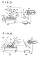
- the distance between the face 30a of the prism 30 and the metal film 12 is kept constant in the manner similar to that in the first embodiment.
Landscapes
- Physics & Mathematics (AREA)
- Health & Medical Sciences (AREA)
- Life Sciences & Earth Sciences (AREA)
- Chemical & Material Sciences (AREA)
- Analytical Chemistry (AREA)
- Biochemistry (AREA)
- General Health & Medical Sciences (AREA)
- General Physics & Mathematics (AREA)
- Immunology (AREA)
- Pathology (AREA)
- Investigating Or Analysing Materials By Optical Means (AREA)
- Length Measuring Devices By Optical Means (AREA)
Claims (3)
- Oberflächenplasinonensensor, umfassend:gekennzeichnet durch eine Abstandsmessungs-Lichtquelle (21), die einen Abstandsmessungs-Lichtstrahl (20) mit einer Wellenlänge, die von dem Metallfilm (12) absorbiert werden kann, dazu bringt, derart in den dielektrischen Block (10, 30, 60, 62) einzutreten, daß der Abstandsmessungs-Lichtstrahl (20) mit Totalreflexion an der einen Seite (10a, 30a, 62a) des dielektrischen Blocks (10, 30, 60, 62) reflektiert wird,einen dielektrischen Block (10, 30, 60, 62),einen Metallfilm (12) mit einer Probenaufnahmeseite, die einer Seite (10a; 30a, 62a) des dielektrischen Blocks (10, 30, 60, 62) mit Abstand von diesem zugewandt ist, und auf der eine Probe (11) plaziert ist,eine einen Lichtstrahl (13) emittierende Lichtquelle (14),eine Optik (15), die den Lichtstrahl (13) dazu bringt, in den dielektrischen Block (10, 30, 60, 62) einzutreten, so daß der Lichtstrahl (13) mittels Totalreflexion an der einen Seite (10a, 30a, 62a) des dielektrischen Blocks (10, 30, 60, 62) reflektiert wird und verschiedene Einfallwinkel des Lichtstrahls an der einen Seite des dielektrischen Blocks (10, 30, 60, 62) einschließlich eines Einfallwinkels, bei dem Oberflächenplasmon erzeugt wird, erhalten werden können, undeine Detektoreinrichtung (16), die den Einfallwinkel des Lichtstrahls detektiert, bei welchem Dämpfung der Totalreflexion stattfindet und die Menge reflektierten Lichts verringert ist,
eine Antriebseinrichtung (22, 23), welche den dielektrischen Block (10, 30, 60, 62) und den Metallfilm (12) relativ zueinander bewegt, so daß der Abstand zwischen der einen Seite (10a, 30a, 62a) des dielektrischen Blocks (10, 30; 60, 62) und der Probenaufnahmeseite des Metallfilms sich ändert,
einen Photodetektor (24), der das Maß des Abstandsmessungs-Lichtstrahls (20) mißt, der mit Totalreflexion an der einen Seite (10a; 30a; 62a) des dielektrischen Blocks (10; 30; 60; 62) reflektiert wird, und
eine Steuereinrichtung (26), die die Antriebseinrichtung (22, 23) so steuert, daß sie den dielektrischen Block (10; 30; 60; 62) und den Metallfilm (12) relativ zueinander derart bewegt, daß das Maß des reflektierten Abstandsmessungs-Lichtstrahls, wie es von dem Photodetektor (24) detektiert wird, konstant gehalten wird. - Sensor nach Anspruch 1, bei dem der dielektrische Block (10, 30) wie ein Prisma geformt ist.
- Sensor nach Anspruch 1, bei dem der dielektrische Block (62) mit einem Prisma (60) integriert ist, wobei zwischen den Teilen sich ein Brechungsindex-Anpaßfluid (61) befindet, wobei der dielektrische Block (62), das Prisma (60) und das Brechungsindex-Anpaßfluid (61) einander im Brechungsindex gleichen und die Lichtstrahlen (13, 20) dazu gebracht werden, in das Prisma (60) einzutreten, um mit Totalreflexion an einer Seite des dielektrischen Blocks (62) reflektiert zu werden.
Applications Claiming Priority (4)
| Application Number | Priority Date | Filing Date | Title |
|---|---|---|---|
| JP11865898 | 1998-04-28 | ||
| JP11865898 | 1998-04-28 | ||
| JP2100399A JP3343086B2 (ja) | 1998-04-28 | 1999-01-29 | 表面プラズモンセンサー |
| JP02100399 | 1999-01-29 |
Publications (3)
| Publication Number | Publication Date |
|---|---|
| EP0953836A2 EP0953836A2 (de) | 1999-11-03 |
| EP0953836A3 EP0953836A3 (de) | 2000-08-09 |
| EP0953836B1 true EP0953836B1 (de) | 2004-07-07 |
Family
ID=26358011
Family Applications (1)
| Application Number | Title | Priority Date | Filing Date |
|---|---|---|---|
| EP19990108241 Expired - Lifetime EP0953836B1 (de) | 1998-04-28 | 1999-04-27 | Oberflächenplasmonensensor |
Country Status (4)
| Country | Link |
|---|---|
| US (1) | US6208422B1 (de) |
| EP (1) | EP0953836B1 (de) |
| JP (1) | JP3343086B2 (de) |
| DE (1) | DE69918488T2 (de) |
Families Citing this family (15)
| Publication number | Priority date | Publication date | Assignee | Title |
|---|---|---|---|---|
| EP0935131A3 (de) * | 1998-02-05 | 2000-03-15 | Fuji Photo Film Co., Ltd. | Oberflächenplasmonenresonanz-Sensor mit wellenlängenstabilisierter Laserlichtquelle |
| JP3706265B2 (ja) * | 1998-12-21 | 2005-10-12 | 富士写真フイルム株式会社 | 表面プラズモンセンサー |
| US6529277B1 (en) * | 2000-07-07 | 2003-03-04 | California Institute Of Technology | Optical devices based on resonant configurational effects |
| EP1373872A4 (de) * | 2001-02-26 | 2009-04-22 | Yeda Res & Dev | Verfahren und vorrichtung zum nachweis und zur quantifizierung einer chemischen substanz unter verwendung einer spektraleigenschaft metallischer inseln |
| US6697158B2 (en) * | 2001-04-03 | 2004-02-24 | Fuji Photo Film Co., Ltd. | Measuring apparatus utilizing attenuated total reflection |
| JP2002365210A (ja) * | 2001-06-11 | 2002-12-18 | Hitachi Ltd | 生体分子検出方法 |
| DE10163657B4 (de) * | 2001-12-21 | 2008-05-08 | Gedig, Erk, Dr. | Vorrichtung und Verfahren zur Untersuchung dünner Schichten |
| DE602004025073D1 (de) | 2003-09-02 | 2010-03-04 | Fujifilm Corp | Messgerät basierend auf der Oberflächenplasmonenresonanz |
| CN102253014A (zh) * | 2011-04-15 | 2011-11-23 | 深圳大学 | 表面等离子体共振传感检测系统和方法 |
| JP6415931B2 (ja) * | 2014-10-31 | 2018-10-31 | 旭化成株式会社 | テラヘルツ波測定装置、及び、テラヘルツ波測定方法 |
| US10197793B2 (en) * | 2016-05-12 | 2019-02-05 | The Chinese University Of Hong Kong | Light modulator using total internal reflection at an interface with a tunable conductive layer |
| JP6782926B2 (ja) * | 2016-08-17 | 2020-11-11 | 国立研究開発法人産業技術総合研究所 | 被検体解析装置 |
| CN106403830B (zh) * | 2016-09-26 | 2018-11-20 | 中国科学院上海光学精密机械研究所 | 椭偏仪测量超薄膜层的精度提升方法和装置 |
| JP6843013B2 (ja) * | 2017-07-19 | 2021-03-17 | 浜松ホトニクス株式会社 | テラヘルツ波分光計測装置およびテラヘルツ波分光計測方法 |
| US12480874B2 (en) * | 2021-01-28 | 2025-11-25 | Universidad De Los Andes | Plasmonic device, system and method |
Family Cites Families (12)
| Publication number | Priority date | Publication date | Assignee | Title |
|---|---|---|---|---|
| JPS55159105A (en) * | 1979-05-29 | 1980-12-11 | Ibm | Thickness measuring method of dielectric film |
| FR2654212A1 (fr) * | 1989-11-03 | 1991-05-10 | Ardt | Procede d'analyse spectroscopique ponctuelle de la lumiere diffractee ou absorbee par une substance placee dans un champ proche, et microscopes optiques a balayage en champ proche mettant en óoeuvre ce procede. |
| US5075551A (en) * | 1990-03-12 | 1991-12-24 | Fuji Electric Co., Ltd. | Infrared absorption enhanced spectroscopic apparatus |
| JPH03261846A (ja) * | 1990-03-12 | 1991-11-21 | Fuji Electric Co Ltd | 赤外線吸収強化分光装置 |
| JP2578026B2 (ja) * | 1991-04-30 | 1997-02-05 | 大日本スクリーン製造株式会社 | 光学測定装置 |
| US5239183A (en) * | 1991-04-30 | 1993-08-24 | Dainippon Screen Mfg. Co., Ltd. | Optical gap measuring device using frustrated internal reflection |
| JPH06167443A (ja) | 1992-10-23 | 1994-06-14 | Olympus Optical Co Ltd | 表面プラズモン共鳴を利用した測定装置 |
| JP3365809B2 (ja) * | 1993-03-15 | 2003-01-14 | オリンパス光学工業株式会社 | 表面プラズモン共鳴を利用した測定装置 |
| US5633492A (en) * | 1995-04-17 | 1997-05-27 | Ceram Optec Industries, Inc. | Real time monitoring of changes in objects or media |
| JPH09257696A (ja) * | 1996-03-19 | 1997-10-03 | Toto Ltd | 表面プラズモン共鳴センサ装置 |
| US5917607A (en) * | 1996-04-25 | 1999-06-29 | Fuji Photo Film Co., Ltd. | Surface plasmon sensor for multiple channel analysis |
| EP1650550B1 (de) * | 1996-04-30 | 2012-10-17 | FUJIFILM Corporation | Oberflächenplasmonensensor |
-
1999
- 1999-01-29 JP JP2100399A patent/JP3343086B2/ja not_active Expired - Fee Related
- 1999-04-27 EP EP19990108241 patent/EP0953836B1/de not_active Expired - Lifetime
- 1999-04-27 DE DE1999618488 patent/DE69918488T2/de not_active Expired - Lifetime
- 1999-04-28 US US09/301,126 patent/US6208422B1/en not_active Expired - Lifetime
Also Published As
| Publication number | Publication date |
|---|---|
| EP0953836A2 (de) | 1999-11-03 |
| US6208422B1 (en) | 2001-03-27 |
| EP0953836A3 (de) | 2000-08-09 |
| JP2000019104A (ja) | 2000-01-21 |
| DE69918488D1 (de) | 2004-08-12 |
| JP3343086B2 (ja) | 2002-11-11 |
| DE69918488T2 (de) | 2004-11-25 |
Similar Documents
| Publication | Publication Date | Title |
|---|---|---|
| US6577396B1 (en) | Surface plasmon sensor | |
| US6208422B1 (en) | Surface plasmon sensor | |
| US6791691B2 (en) | Measuring method and apparatus using attenuation in total internal reflection | |
| US6597456B2 (en) | Measuring chip for quantitative analysis of substances | |
| US6885454B2 (en) | Measuring apparatus | |
| EP1324019B1 (de) | Sensorsystem mit evaneszenten Wellen | |
| EP1512962B1 (de) | Messgerät | |
| US7187444B2 (en) | Measuring method and apparatus using attenuation in total internal reflection | |
| US7586615B2 (en) | Measuring unit | |
| US6891620B2 (en) | Measuring plate | |
| JP2000180353A (ja) | 表面プラズモンセンサー | |
| US7317534B2 (en) | Measuring method and system | |
| US7009706B2 (en) | Measuring chip | |
| US6697158B2 (en) | Measuring apparatus utilizing attenuated total reflection | |
| US20050046854A1 (en) | Measuring apparatus and sensor unit for same | |
| EP1566628B1 (de) | Messvorrichtung | |
| JP3761080B2 (ja) | 全反射減衰を利用した測定方法および測定装置 | |
| JPH10281982A (ja) | 表面プラズモンセンサー | |
| JPH1078391A (ja) | 表面プラズモンセンサー | |
| JP2002195942A (ja) | 全反射減衰を利用したセンサー | |
| JP2002048707A (ja) | 全反射減衰を利用した測定方法および装置 | |
| JP4014805B2 (ja) | 全反射減衰を利用したセンサー | |
| CN112630194A (zh) | 一种基于扫描振镜的角度调制型spr传感器及spr检测设备 | |
| JP2003139692A (ja) | 全反射減衰を利用したセンサー | |
| JP2004085488A (ja) | 測定装置 |
Legal Events
| Date | Code | Title | Description |
|---|---|---|---|
| PUAI | Public reference made under article 153(3) epc to a published international application that has entered the european phase |
Free format text: ORIGINAL CODE: 0009012 |
|
| AK | Designated contracting states |
Kind code of ref document: A2 Designated state(s): DE FR GB |
|
| AX | Request for extension of the european patent |
Free format text: AL;LT;LV;MK;RO;SI |
|
| PUAL | Search report despatched |
Free format text: ORIGINAL CODE: 0009013 |
|
| AK | Designated contracting states |
Kind code of ref document: A3 Designated state(s): AT BE CH CY DE DK ES FI FR GB GR IE IT LI LU MC NL PT SE |
|
| AX | Request for extension of the european patent |
Free format text: AL;LT;LV;MK;RO;SI |
|
| 17P | Request for examination filed |
Effective date: 20000918 |
|
| AKX | Designation fees paid |
Free format text: DE FR GB |
|
| 17Q | First examination report despatched |
Effective date: 20020715 |
|
| GRAP | Despatch of communication of intention to grant a patent |
Free format text: ORIGINAL CODE: EPIDOSNIGR1 |
|
| GRAS | Grant fee paid |
Free format text: ORIGINAL CODE: EPIDOSNIGR3 |
|
| GRAA | (expected) grant |
Free format text: ORIGINAL CODE: 0009210 |
|
| AK | Designated contracting states |
Kind code of ref document: B1 Designated state(s): DE FR GB |
|
| REG | Reference to a national code |
Ref country code: GB Ref legal event code: FG4D |
|
| REF | Corresponds to: |
Ref document number: 69918488 Country of ref document: DE Date of ref document: 20040812 Kind code of ref document: P |
|
| ET | Fr: translation filed | ||
| PLBE | No opposition filed within time limit |
Free format text: ORIGINAL CODE: 0009261 |
|
| STAA | Information on the status of an ep patent application or granted ep patent |
Free format text: STATUS: NO OPPOSITION FILED WITHIN TIME LIMIT |
|
| 26N | No opposition filed |
Effective date: 20050408 |
|
| REG | Reference to a national code |
Ref country code: GB Ref legal event code: 732E |
|
| REG | Reference to a national code |
Ref country code: FR Ref legal event code: TP Ref country code: FR Ref legal event code: CD |
|
| PGFP | Annual fee paid to national office [announced via postgrant information from national office to epo] |
Ref country code: GB Payment date: 20140423 Year of fee payment: 16 |
|
| PGFP | Annual fee paid to national office [announced via postgrant information from national office to epo] |
Ref country code: DE Payment date: 20140430 Year of fee payment: 16 Ref country code: FR Payment date: 20140409 Year of fee payment: 16 |
|
| REG | Reference to a national code |
Ref country code: DE Ref legal event code: R119 Ref document number: 69918488 Country of ref document: DE |
|
| GBPC | Gb: european patent ceased through non-payment of renewal fee |
Effective date: 20150427 |
|
| PG25 | Lapsed in a contracting state [announced via postgrant information from national office to epo] |
Ref country code: GB Free format text: LAPSE BECAUSE OF NON-PAYMENT OF DUE FEES Effective date: 20150427 Ref country code: DE Free format text: LAPSE BECAUSE OF NON-PAYMENT OF DUE FEES Effective date: 20151103 |
|
| REG | Reference to a national code |
Ref country code: FR Ref legal event code: ST Effective date: 20151231 |
|
| PG25 | Lapsed in a contracting state [announced via postgrant information from national office to epo] |
Ref country code: FR Free format text: LAPSE BECAUSE OF NON-PAYMENT OF DUE FEES Effective date: 20150430 |