EP0954046A2 - Résonateur diélectrique, filtre diélectrique, duplexeur diélectrique, dispositif de communication, et procédé de fabrication d' un résonateur diélectrique - Google Patents
Résonateur diélectrique, filtre diélectrique, duplexeur diélectrique, dispositif de communication, et procédé de fabrication d' un résonateur diélectrique Download PDFInfo
- Publication number
- EP0954046A2 EP0954046A2 EP99108342A EP99108342A EP0954046A2 EP 0954046 A2 EP0954046 A2 EP 0954046A2 EP 99108342 A EP99108342 A EP 99108342A EP 99108342 A EP99108342 A EP 99108342A EP 0954046 A2 EP0954046 A2 EP 0954046A2
- Authority
- EP
- European Patent Office
- Prior art keywords
- dielectric
- resonator
- dielectric resonator
- thin film
- duplexer
- Prior art date
- Legal status (The legal status is an assumption and is not a legal conclusion. Google has not performed a legal analysis and makes no representation as to the accuracy of the status listed.)
- Withdrawn
Links
Images


Classifications
-
- H—ELECTRICITY
- H01—ELECTRIC ELEMENTS
- H01P—WAVEGUIDES; RESONATORS, LINES, OR OTHER DEVICES OF THE WAVEGUIDE TYPE
- H01P1/00—Auxiliary devices
- H01P1/20—Frequency-selective devices, e.g. filters
- H01P1/201—Filters for transverse electromagnetic waves
- H01P1/203—Strip line filters
- H01P1/20309—Strip line filters with dielectric resonator
- H01P1/20318—Strip line filters with dielectric resonator with dielectric resonators as non-metallised opposite openings in the metallised surfaces of a substrate
-
- H—ELECTRICITY
- H01—ELECTRIC ELEMENTS
- H01P—WAVEGUIDES; RESONATORS, LINES, OR OTHER DEVICES OF THE WAVEGUIDE TYPE
- H01P1/00—Auxiliary devices
- H01P1/20—Frequency-selective devices, e.g. filters
- H01P1/201—Filters for transverse electromagnetic waves
- H01P1/205—Comb or interdigital filters; Cascaded coaxial cavities
-
- H—ELECTRICITY
- H01—ELECTRIC ELEMENTS
- H01P—WAVEGUIDES; RESONATORS, LINES, OR OTHER DEVICES OF THE WAVEGUIDE TYPE
- H01P1/00—Auxiliary devices
- H01P1/20—Frequency-selective devices, e.g. filters
- H01P1/213—Frequency-selective devices, e.g. filters combining or separating two or more different frequencies
-
- H—ELECTRICITY
- H01—ELECTRIC ELEMENTS
- H01P—WAVEGUIDES; RESONATORS, LINES, OR OTHER DEVICES OF THE WAVEGUIDE TYPE
- H01P7/00—Resonators of the waveguide type
- H01P7/10—Dielectric resonators
Definitions
- the present invention relates to a dielectric resonator, a dielectric filter, a dielectric duplexer, and a communication device each for use in a communication base station, and a method of producing a dielectric resonator.
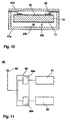
- FIG. 12 is a perspective view of the dielectric resonator.
- FIG. 13 is a partly cross sectional view of one end of the dielectric resonator.
- FIG. 14 is an exploded perspective view of the dielectric filter.
- the filter will be described by use of a two stage band-elimination dielectric filter in which two dielectrics are connected with a quarter-wave line.
- This filter was not a publicly known conventional technique when Japanese Patent Application No. 10-118933, which is a basis of claim of priority for the application of the present invention, was filed.
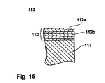
- a dielectric resonator 110 is composed of a columnar dielectric 111, and thin film multi-layers 112 formed on the opposite sides of the dielectric 111.
- the thin film multi-layer electrodes 112 are employed as the electrodes of the dielectric resonator 110, the nonloaded Q of the dielectric resonator 110 is enhanced.
- the dielectric resonator with high characteristics can be provided.
- a dielectric filter 120 is made up of a shield cavity 121 made of iron or the like, two dielectric resonators 110 arranged in the shield cavity 121, and an ground plate 122, electrical probes 123 as external coupling means, and external connectors 124 attached to the shield cavity 121.
- each dielectric resonator 110 are formed of the columnar dielectric 111 having the thin film multi-layer electrodes 112 formed on the opposite sides thereof.
- One electrode surface of the dielectric resonator 110 is soldered to the ground plate 122 having a step 122a and a hole 122b for soldering.
- the ground plate 122 is sandwiched between the body 121a of the shield cavity 121 and a lid 121b.
- the dielectric resonator 110 is arranged in the shield cavity 121.
- one ends of electrical probes 123 are connected to the center conductors of the external connectors 124, respectively, and are elongated in the spaces between the dielectric resonators 110 and the shield cavity 121.
- the center conductors of the two external connectors 124 are connected through a quarter-wave line 125.
- the dielectric filter 120 having the above-described configuration, an input signal, when it is input through the external connectors 124, is transmitted to the electrical probes 123, so that the electrical probes 123 and the dielectric resonators 110 are capacitively coupled. Then, the dielectric resonators 110 resonate at a resonant frequency determined by the shapes and sizes of the dielectric resonators 110.
- the dielectric filter 120 in which the dielectric resonators are connected through the quarter-wave line 125 for connection is provided functions as a band-elimination dielectric filter for eliminating the desired frequency.
- the dielectric resonators In general, a great number of dielectric resonators having a predetermined diameter and thickness are produced at one time. Accordingly, in order that the dielectric resonators are used in dielectric filters of which the frequency characteristics are different, it is necessary to adjust the resonant frequencies of the dielectric resonators in correspondence to the frequencies.
- the peripheral side-face of the dielectric resonator having thin film multi-layer electrodes formed on the opposite sides thereof, including the thin film multi-layer electrodes, are cut, or the thin film multi-layer electrodes are partially cut.
- the peripheral side-face of the dielectric 111 is cut, in the thin film multi-layer electrode 112 comprising metallic layers 112a made of copper or the like and dielectric layers 112b, due to the rolling properties of the metallic layers 112a, a part of the metallic layers 112a of the thin film multi-layer electrode 112 is short circuited, so that the nonloaded Q of the dielectric resonator 110 is reduced. Therefore, after the peripheral side-face is cut to adjust the resonant frequency of the dielectric resonator, etching or the like is required to remove the short circuiting portion of the thin film multi-layer electrode. Thus, the number of production processes is increased.
- a method of cutting the dielectric portion of the dielectric resonator excluding the thin film multi-layer electrode may be proposed.
- it is required to cut an amount of the dielectric.
- the dielectric of the dielectric resonator is partially removed, the symmetric structure of the dielectric resonator is unbalanced, so that the current distribution becomes uneven, and the nonloaded Q of the dielectric resonator is reduced.
- a dielectric resonator, a dielectric filter, a dielectric duplexer, a communication device, and a method of producing the dielectric resonator of the present invention have been devised. Accordingly, it is an object of the present invention to solve the above-described problems and to provide a dielectric resonator, a dielectric filter, a dielectric duplexer, and a communication device each having a high nonloaded Q, and a method of producing the dielectric resonator.
- a dielectric resonator which comprises a substantially columnar dielectric, a thin film multi-layer electrode formed on at least one of two faces opposite to each other of the dielectric, and a concave portion formed substantially evenly on the peripheral side-face of the dielectric.
- a dielectric filter of the present invention comprises a shield cavity with conductive properties, a dielectric resonator, and an external coupling means to be coupled to the dielectric resonator, the dielectric resonator including a substantially columnar dielectric arranged in the shield cavity, a thin film multi-layer electrode formed on at least one of two faces opposite to each other of the dielectric, and a concave portion formed substantially evenly on the peripheral side face of the dielectric.
- a dielectric duplexer of the present invention comprises a shield cavity with electroconductive properties, a dielectric resonator, an external coupling means to be coupled to the dielectric resonator, and an input - output connection means connected to the external coupling means and an antenna connection means, the dielectric resonator including a substantially columnar dielectric arranged in the shield cavity, a thin film multi-layer electrode formed on at least one of two faces opposite to each other of the dielectric, and a concave portion formed substantially evenly on the peripheral side face of the dielectric.
- a communication device of the present invention comprises a dielectric duplexer, one of a transmission circuit and a receiving circuit connected to the dielectric duplexer, and an antenna connected to said dielectric duplexer, the dielectric duplexer including a shield cavity with conductive properties, a dielectric resonator, an external coupling means to be coupled to the dielectric resonator, an input - output connection means connected to the external coupling means and an antenna connection means, the dielectric resonator including a substantially columnar dielectric arranged in the shield cavity, a thin film multi-layer electrode formed on at least one of two faces opposite to each other of the dielectric, and a concave portion formed substantially evenly on the peripheral side-face of the resonator.
- the symmetrical structure of the dielectric resonator is kept, the current distribution is not disturbed. Further, the thin film multi-layer electrode formed in the dielectric resonator is prevented from being short-circuited.
- a method of producing a dielectric resonator comprises the steps of: forming a thin film multi-layer electrode at least one of two faces opposite to each other of a substantially columnar dielectric and an electrode on the other face, and fixing the dielectric to a rotation apparatus, and rotating the dielectric to cut substantially evenly the peripheral side-face of the dielectric by use of a cutting means.
- the dielectric resonator of which the symmetrical structure can be easily kept can be produced without the thin film multi-layer electrode short-circuited.
- FIG. 1 is a perspective view of the dielectric resonator
- FIG. 2 is a cross sectional view taken on line X - X of FIG. 1.
- dielectric resonators 10 of the instant embodiment each is made up of a columnar dielectric 11, thin film multi-layer electrodes 12 formed on two faces opposite to each other of the dielectric 11, and a concave portion 13 substantially evenly formed on the peripheral side-face of the dielectric 11. With the depth and width of the concave portion 13, the resonant frequency of the dielectric resonator 10 is adjusted.
- the dielectric resonator 10 obtained by forming the thin film multi-layer electrodes 12 on the two faces opposite to each other of the columnar dielectric 11, is mounted on a rotation apparatus 14.
- the rotation apparatus 14 is equipped with a suction means for sucking the dielectric resonator 10 from below.
- the dielectric resonator 10 is fixed by means of the sucking means.
- the rotation apparatus 14 is rotated in the horizontal direction, and thereby, the dielectric resonator 10 is also rotated in the horizontal direction.
- a diamond bar 15 having a disk shape under rotation is pressed to the side-face of the dielectric resonator 10 which is also under rotation.
- the dielectric resonator 10 having a concave portion 13 substantially evenly formed on the peripheral side-face thereof excluding the thin film multi-layer electrodes 12, as shown in FIGS. 1 and 2, can be easily formed. If the diamond bar 15 having a spherical shape is used as the cutting means, the dielectric resonator 10c with the concave portion 13a having a concave shape as shown in the cross sectional view of FIG. 4.
- the resonant frequency of the dielectric resonator 10 can be adjusted without the thin film multi-layer electrodes 12 short-circuited, and thereby, it is unnecessary to carry out the etching of the thin film multi-layer electrodes 12 after the peripheral side-face is cut.
- the concave portion 13 on the peripheral side-face of the dielectric resonator 10 is formed substantially evenly there, the symmetric structure of the dielectric resonator 10 is not unbalanced, and the current distribution is prevented from being disturbed. Accordingly, the reduction of the nonloaded Q of the dielectric resonator 10 is prevented.
- FIG. 5 is an exploded perspective view of the dielectric filter of the instant embodiment.
- FIG. 6 is a cross sectional view taken on line Y-Y of FIG. 5.
- a two-stage band-elimination filter in which two dielectrics arranged laterally are connected through a quarter-wave line.
- a dielectric filter 20 of the instant embodiment is made up of a shield cavity 21 made of iron plated with silver, two dielectric resonators 10 having a columnar shape arranged in the shield cavities 21, an ground plate 22, electrical probes 23 as external coupling means, and external connectors 24 attached to the shield cavities 21, respectively.
- the thin film multi-layer electrodes 12 are formed on two faces opposite to each other of the dielectric resonator 10.
- the ground plate 22 made of a copper sheet plated with silver, having steps 22a and holes 22b for soldering plated with silver is soldered to one of the two faces.
- the ground plate 22 is sandwiched between the body 21a of the shield cavity 21 and the lid 21b in such a manner that the ground plate 22 is in conduction with the shield cavity 21.
- the dielectric resonators 10 are arranged in the shield cavities 21.
- Electrical probes 23 made of metallic wires are arranged, elongating in the spaces between the electric resonators 10 and the shield cavity 21, respectively. One end of the electrical probe 23 is attached to an external connector 24 fixed to the shield cavity 21.
- the center conductors of the two external connectors 24 are connected through the quarter-wave line 25.
- the concave portions 13 are substantially evenly formed on the peripheral side-faces of the dielectric resonators 10 arranged in the shield cavities 21, other than the thin film multi-layer electrodes 12.
- the resonant frequency of the dielectric resonators 10 can be adjusted while the symmetric structure of the dielectric resonators 10 is kept, namely, the current distribution of the dielectric resonators 10 is not prevented from being disturbed.
- the reduction of the nonloaded Q is prevented.
- the dielectric filter 20 having the above-described structure, an input signal when it is input through the external connector 24 is fed to the electrical probe 23, so that the electrical probe 23 and the dielectric resonator 10 are capacitive-coupled.
- the dielectric resonators 10 become resonated.
- the dielectric filter 20 in which the dielectric resonators are connected through the quarter-wave line 25 functions as a two stage band-elimination filter for eliminating desired frequency waves.
- a fine amount of the dielectric may be cut from holes 26 provided in the shield cavity 21 by means of a fluter or the like.
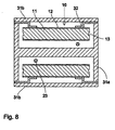
- FIG. 7 is an exploded perspective view of the dielectric filter of the instant embodiment.
- FIG. 8 is a cross sectional view taken on line Z - Z of FIG. 7.
- Like numerals refer to like parts in the instant and above-described embodiments, and detailed description of the like parts will be omitted below.
- the dielectric filter 30 is made up of a shield cavity 31 made of iron plated with silver, two columnar dielectric resonators 10 arranged in the shield cavity 31, an ground plate 32, an electrical probe 23 as an external coupling means, and an external connector 24 attached to the shield cavity 31.
- the difference between the instant and above-described embodiments lies in that the two electric resonators 10 are laterally arranged in the above-described embodiment, while in the instant embodiment, the dielectric resonators 31 are arranged on the front and back sides of the shield cavity 31.
- the height of the dielectric filter is reduced, while in the instant embodiment, the area of the dielectric filter 30 can be reduced.
- the concave portion 13 is formed substantially evenly on the peripheral side-face of the dielectric resonator 10 excluding the thin film multi-layer electrodes 12.
- the resonant frequency of the dielectric resonator 10 can be adjusted while the symmetrical structure of the dielectric resonator 10 is kept, that is, the current distribution of the dielectric resonator 10 is prevented from being disturbed.
- the reduction of the nonloaded Q is prevented.
- the dielectric filter 30 having the above configuration, an input signal when it is input through the external connector 24 is fed to the electrical probe 23, so that the electrical probe 23 and the dielectric resonator 10 are capacitive-coupled. Then, at the resonant frequency determined by the shape and size of the dielectric resonator 10, the arrangement of the dielectric resonator 10, and the like, the dielectric resonator 10 becomes resonated.
- the dielectric filter 30 in which the dielectric resonators are connected to each other through the quarter-wave line 25 functions as a two-stage band-elimination dielectric filter for eliminating desired frequency waves.
- FIG. 9 is an exploded perspective view of the dielectric duplexer of the instant embodiment.
- FIG. 10 is a cross sectional view taken on line W - W of FIG. 9.
- Like numerals refer to like parts in the instant and above-described embodiments. Detailed description of the like parts will be omitted below.
- the dielectric duplexer 40 of the instant embodiment includes a first dielectric filter 50a made up of two columnar dielectric resonators parts 10a arranged in the shield cavity 41, and a second dielectric filter 50b made up of another two columnar dielectric resonator parts 10b.
- the two dielectric resonators 10a making up the first dielectric filter part 50a are capacitive-coupled through a coupling member 27a whereby a transmission band pass filter is produced.
- the two dielectric resonators 10b making up the second dielectric filter part 50b has a resonant frequency different from the dielectric resonator 10a of the first dielectric filter part 50a, and capacitive-coupled through a coupling member 27b, whereby a receiving band-pass filter is produced.
- An electrical probe 23a as an external coupling means to be coupled to the dielectric resonator 10a is connected to an external connector 24a and further connected to an external transmission circuit.
- the electrical probe 23b to be coupled to the dielectric resonator 10b of the second dielectric filter part 50b is connected to an external connector 24b, and further connected to an external receiving circuit.
- the electrical probes 23c to be coupled to the dielectric resonator 10a of the first dielectric filter part 50a, and an electrical probe 23d to be coupled with the dielectric resonator 10b of the second dielectric filter part 50b is connected to an external connector 24c and further connected to an external antenna.
- the dielectric duplexer 40 having the above configuration, a predetermined frequency wave is made to pass through the first dielectric filter part 50a, and moreover, a frequency wave different from the above frequency wave is caused to pass through the second dielectric filter 50b.
- the dielectric duplexer 40 functions as a band-pass dielectric duplexer.
- the substantially even concave portion 13 is formed on the peripheral side-faces of the dielectric resonators 10b arranged in the shield cavity 41, excluding the thin film multi-layer electrodes 12.
- the resonant frequency of the dielectric resonators 10b can be adjusted while the symmetrical structure of the dielectric resonator 10b is kept, that is, without disturbances in the current distribution of the dielectric resonators 10b. That is, the nonloaded Q is not reduced. This is true of the dielectric resonators 10a.
- FIG. 11 is a schematic view of the communication device of the instant embodiment.
- a communication device 60 of the instant embodiment is made up of a dielectric duplexer 40, a transmitting circuit 61, a receiving circuit 62, and an antenna 63.
- the dielectric duplexer 40 is the same that is described in the above embodiment.
- the external connector 24a connected to the first dielectric filter part 50a in FIG. 9 is connected to a transmitting circuit 61.
- the external connector 24b connected to the second dielectric filter part 50b is connected to a receiving circuit 62.
- the external connector 24c is connected to an antenna 63.
- a substantially even concave portion is formed on the peripheral side-face of each dielectric resonator arranged in the shield cavity, excluding the thin film multi-layer electrode.
- the substantially even concave portion is formed on the peripheral side face of each dielectric resonator containing the columnar dielectric having the thin film multi-layer electrodes formed on the opposite sides of the dielectric, the peripheral side faces not containing the thin film multi-layer electrodes.
- the resonant frequency can be adjusted with the depth and width of the concave portion without the thin film multi-layer electrodes short-circuited.
- the dielectric resonator with a high non-loading Q factor can be provided.
- the dielectric filter, the dielectric duplexer, and the communication device each having high characteristics can be provided.
- the method of producing the dielectric resonator comprises securing the dielectric resonator to the rotation apparatus, and substantially evenly cutting the peripheral side-face of the dielectric resonator with a cutting means.
- the resonant frequency can be easily adjusted without the thin film multi-layer electrodes formed on the two side opposite to each other of the dielectric resonator short-circuited.
- processes such as etching or the like are unnecessary.
Landscapes
- Physics & Mathematics (AREA)
- Electromagnetism (AREA)
- Control Of Motors That Do Not Use Commutators (AREA)
Applications Claiming Priority (2)
| Application Number | Priority Date | Filing Date | Title |
|---|---|---|---|
| JP11893398 | 1998-04-28 | ||
| JP10118933A JPH11312910A (ja) | 1998-04-28 | 1998-04-28 | 誘電体共振器、誘電体フィルタ、誘電体デュプレクサおよび通信機装置ならびに誘電体共振器の製造方法 |
Publications (2)
| Publication Number | Publication Date |
|---|---|
| EP0954046A2 true EP0954046A2 (fr) | 1999-11-03 |
| EP0954046A3 EP0954046A3 (fr) | 2000-11-29 |
Family
ID=14748822
Family Applications (1)
| Application Number | Title | Priority Date | Filing Date |
|---|---|---|---|
| EP99108342A Withdrawn EP0954046A3 (fr) | 1998-04-28 | 1999-04-28 | Résonateur diélectrique, filtre diélectrique, duplexeur diélectrique, dispositif de communication, et procédé de fabrication d' un résonateur diélectrique |
Country Status (8)
| Country | Link |
|---|---|
| US (1) | US6211755B1 (fr) |
| EP (1) | EP0954046A3 (fr) |
| JP (1) | JPH11312910A (fr) |
| KR (1) | KR19990083562A (fr) |
| CN (1) | CN1121734C (fr) |
| CA (1) | CA2270309C (fr) |
| NO (1) | NO320930B1 (fr) |
| TW (1) | TW419855B (fr) |
Cited By (1)
| Publication number | Priority date | Publication date | Assignee | Title |
|---|---|---|---|---|
| WO2018107478A1 (fr) * | 2016-12-16 | 2018-06-21 | 华为技术有限公司 | Résonateur diélectrique et filtre diélectrique, émetteur-récepteur et station de base l'utilisant |
Families Citing this family (6)
| Publication number | Priority date | Publication date | Assignee | Title |
|---|---|---|---|---|
| US6937118B2 (en) * | 2002-04-01 | 2005-08-30 | Murata Manufacturing Co., Ltd. | High-frequency circuit device, resonator, filter, duplexer, and high-frequency circuit apparatus |
| JPWO2006062082A1 (ja) * | 2004-12-07 | 2008-06-12 | 松下電器産業株式会社 | 薄膜弾性波共振子 |
| US7777598B2 (en) * | 2008-04-14 | 2010-08-17 | Radio Frequency Systems, Inc. | Dielectric combine cavity filter having ceramic resonator rods suspended by polymer wedge mounting structures |
| GB2487872B (en) * | 2012-05-09 | 2012-12-26 | Protean Electric Ltd | An electric motor or generator system |
| WO2016047531A1 (fr) * | 2014-09-24 | 2016-03-31 | 京セラ株式会社 | Résonateur, filtre, et dispositif de communication |
| US10985435B2 (en) * | 2018-07-20 | 2021-04-20 | The Boeing Company | Tunable probe for high-performance cross-coupled RF filters |
Family Cites Families (14)
| Publication number | Priority date | Publication date | Assignee | Title |
|---|---|---|---|---|
| JPS61136302A (ja) * | 1984-12-06 | 1986-06-24 | Murata Mfg Co Ltd | 誘電体共振器 |
| US4706052A (en) * | 1984-12-10 | 1987-11-10 | Murata Manufacturing Co., Ltd. | Dielectric resonator |
| JPH02150808U (fr) * | 1989-05-22 | 1990-12-27 | ||
| JP2509162Y2 (ja) * | 1989-08-31 | 1996-08-28 | 日本特殊陶業株式会社 | 誘電体共振器装置 |
| US5004992A (en) * | 1990-05-25 | 1991-04-02 | Motorola, Inc. | Multi-resonator ceramic filter and method for tuning and adjusting the resonators thereof |
| JP2809555B2 (ja) | 1992-05-15 | 1998-10-08 | 日本特殊陶業株式会社 | 誘電体共振器の周波数調整方法 |
| WO1995006336A1 (fr) * | 1993-08-27 | 1995-03-02 | Murata Manufacturing Co., Ltd. | Electrode multicouche a couches minces utilisee pour le couplage de champs electromagnetiques a hautes frequences |
| US5714919A (en) * | 1993-10-12 | 1998-02-03 | Matsushita Electric Industrial Co., Ltd. | Dielectric notch resonator and filter having preadjusted degree of coupling |
| JPH07111404A (ja) * | 1993-10-13 | 1995-04-25 | Murata Mfg Co Ltd | 誘電体共振器 |
| JP3475555B2 (ja) | 1995-03-02 | 2003-12-08 | 株式会社村田製作所 | Tmモード誘電体共振器、tmモード誘電体共振器装置及び高周波帯域通過フィルタ装置 |
| JP3087651B2 (ja) * | 1996-06-03 | 2000-09-11 | 株式会社村田製作所 | 薄膜多層電極、高周波伝送線路、高周波共振器及び高周波フィルタ |
| JPH1056307A (ja) * | 1996-08-07 | 1998-02-24 | Taiyo Yuden Co Ltd | 誘電体共振器の製造方法 |
| JPH1070403A (ja) * | 1996-08-27 | 1998-03-10 | Fuji Elelctrochem Co Ltd | コムライン型の誘電体フィルタ |
| JPH1127016A (ja) * | 1997-06-30 | 1999-01-29 | Taiyo Yuden Co Ltd | 誘電体円筒共振器の製造方法 |
-
1998
- 1998-04-28 JP JP10118933A patent/JPH11312910A/ja active Pending
-
1999
- 1999-04-23 TW TW088106489A patent/TW419855B/zh active
- 1999-04-27 CA CA002270309A patent/CA2270309C/fr not_active Expired - Lifetime
- 1999-04-27 NO NO19992013A patent/NO320930B1/no not_active IP Right Cessation
- 1999-04-28 EP EP99108342A patent/EP0954046A3/fr not_active Withdrawn
- 1999-04-28 KR KR1019990015191A patent/KR19990083562A/ko not_active Ceased
- 1999-04-28 CN CN99105381A patent/CN1121734C/zh not_active Expired - Lifetime
- 1999-04-28 US US09/301,250 patent/US6211755B1/en not_active Expired - Lifetime
Cited By (1)
| Publication number | Priority date | Publication date | Assignee | Title |
|---|---|---|---|---|
| WO2018107478A1 (fr) * | 2016-12-16 | 2018-06-21 | 华为技术有限公司 | Résonateur diélectrique et filtre diélectrique, émetteur-récepteur et station de base l'utilisant |
Also Published As
| Publication number | Publication date |
|---|---|
| NO320930B1 (no) | 2006-02-13 |
| CN1239337A (zh) | 1999-12-22 |
| JPH11312910A (ja) | 1999-11-09 |
| CA2270309A1 (fr) | 1999-10-28 |
| NO992013D0 (no) | 1999-04-27 |
| CN1121734C (zh) | 2003-09-17 |
| CA2270309C (fr) | 2001-09-18 |
| US6211755B1 (en) | 2001-04-03 |
| NO992013L (no) | 1999-10-29 |
| KR19990083562A (ko) | 1999-11-25 |
| EP0954046A3 (fr) | 2000-11-29 |
| TW419855B (en) | 2001-01-21 |
Similar Documents
| Publication | Publication Date | Title |
|---|---|---|
| US6686815B1 (en) | Microwave filter | |
| EP0997973B1 (fr) | Antenne à filtre et appareil radio utilisant cette antenne | |
| US4827266A (en) | Antenna with lumped reactive matching elements between radiator and groundplate | |
| US6549095B2 (en) | Dielectric filter, dielectric duplexer, and communication apparatus | |
| JP3750335B2 (ja) | 帯域阻止誘電体フィルタ、誘電体デュプレクサおよび通信機装置 | |
| JPS58103202A (ja) | 誘電体フイルタ | |
| CA2270309C (fr) | Resonateur, filtre et duplexeur dielectriques, dispositif de communication et methode de fabrication d'un resonateur dielectrique | |
| US6597263B2 (en) | Dielectric filter having notch pattern | |
| EP0917231B1 (fr) | Filtre diélectrique, duplexeur diélectrique, et dispositif de communication | |
| EP0930666B1 (fr) | Filtre diélectrique et duplexeur diélectrique | |
| EP1315228A1 (fr) | Filtre dielectrique | |
| CN111430871A (zh) | 一种介质谐振器、介质滤波器、收发信机及基站 | |
| JPH11127002A (ja) | 誘電体フィルタ | |
| EP0966055A1 (fr) | Filtre diélectrique, dispositif de partage d' émission/réception, et appareil de communication | |
| JP2004364248A (ja) | 誘電体フィルタ、誘電体デュプレクサおよび通信装置 | |
| JP3468093B2 (ja) | 誘電体フィルタ、共用器および電子機器 | |
| JPS6150522B2 (fr) | ||
| JP3009331B2 (ja) | 広帯域誘電体フィルタ | |
| JPH09167902A (ja) | 誘電体フィルタ | |
| JP2842230B2 (ja) | 誘電体同軸共振器 | |
| JP2001211005A (ja) | 誘電体デュプレクサとその周波数調整方法 | |
| KR20020045228A (ko) | 유전체공진기를 이용한 듀플렉서 | |
| JPH0134402B2 (fr) | ||
| JPH05167306A (ja) | 導電性の障壁を設けた誘電体帯域通過フィルタ | |
| JP2005150927A (ja) | 誘電体フィルタ、誘電体デュプレクサおよび通信装置 |
Legal Events
| Date | Code | Title | Description |
|---|---|---|---|
| PUAI | Public reference made under article 153(3) epc to a published international application that has entered the european phase |
Free format text: ORIGINAL CODE: 0009012 |
|
| 17P | Request for examination filed |
Effective date: 19990428 |
|
| AK | Designated contracting states |
Kind code of ref document: A2 Designated state(s): DE FI GB SE |
|
| AX | Request for extension of the european patent |
Free format text: AL;LT;LV;MK;RO;SI |
|
| PUAL | Search report despatched |
Free format text: ORIGINAL CODE: 0009013 |
|
| AK | Designated contracting states |
Kind code of ref document: A3 Designated state(s): AT BE CH CY DE DK ES FI FR GB GR IE IT LI LU MC NL PT SE |
|
| AX | Request for extension of the european patent |
Free format text: AL;LT;LV;MK;RO;SI |
|
| AKX | Designation fees paid |
Free format text: DE FI GB SE |
|
| 17Q | First examination report despatched |
Effective date: 20050214 |
|
| GRAP | Despatch of communication of intention to grant a patent |
Free format text: ORIGINAL CODE: EPIDOSNIGR1 |
|
| STAA | Information on the status of an ep patent application or granted ep patent |
Free format text: STATUS: THE APPLICATION IS DEEMED TO BE WITHDRAWN |
|
| 18D | Application deemed to be withdrawn |
Effective date: 20070425 |
|
| RAP1 | Party data changed (applicant data changed or rights of an application transferred) |
Owner name: MURATA MANUFACTURING CO., LTD. |