EP0955704A2 - Dispositif de conversion photo-électrique et méthode de fabrication - Google Patents
Dispositif de conversion photo-électrique et méthode de fabrication Download PDFInfo
- Publication number
- EP0955704A2 EP0955704A2 EP99108868A EP99108868A EP0955704A2 EP 0955704 A2 EP0955704 A2 EP 0955704A2 EP 99108868 A EP99108868 A EP 99108868A EP 99108868 A EP99108868 A EP 99108868A EP 0955704 A2 EP0955704 A2 EP 0955704A2
- Authority
- EP
- European Patent Office
- Prior art keywords
- photoelectric conversion
- electrode
- contact electrode
- conversion element
- substrate
- Prior art date
- Legal status (The legal status is an assumption and is not a legal conclusion. Google has not performed a legal analysis and makes no representation as to the accuracy of the status listed.)
- Granted
Links
Images


Classifications
-
- H—ELECTRICITY
- H10—SEMICONDUCTOR DEVICES; ELECTRIC SOLID-STATE DEVICES NOT OTHERWISE PROVIDED FOR
- H10H—INORGANIC LIGHT-EMITTING SEMICONDUCTOR DEVICES HAVING POTENTIAL BARRIERS
- H10H20/00—Individual inorganic light-emitting semiconductor devices having potential barriers, e.g. light-emitting diodes [LED]
- H10H20/80—Constructional details
- H10H20/83—Electrodes
- H10H20/831—Electrodes characterised by their shape
-
- H—ELECTRICITY
- H01—ELECTRIC ELEMENTS
- H01S—DEVICES USING THE PROCESS OF LIGHT AMPLIFICATION BY STIMULATED EMISSION OF RADIATION [LASER] TO AMPLIFY OR GENERATE LIGHT; DEVICES USING STIMULATED EMISSION OF ELECTROMAGNETIC RADIATION IN WAVE RANGES OTHER THAN OPTICAL
- H01S5/00—Semiconductor lasers
- H01S5/02—Structural details or components not essential to laser action
- H01S5/022—Mountings; Housings
- H01S5/0235—Method for mounting laser chips
- H01S5/02375—Positioning of the laser chips
-
- H—ELECTRICITY
- H01—ELECTRIC ELEMENTS
- H01S—DEVICES USING THE PROCESS OF LIGHT AMPLIFICATION BY STIMULATED EMISSION OF RADIATION [LASER] TO AMPLIFY OR GENERATE LIGHT; DEVICES USING STIMULATED EMISSION OF ELECTROMAGNETIC RADIATION IN WAVE RANGES OTHER THAN OPTICAL
- H01S5/00—Semiconductor lasers
- H01S5/04—Processes or apparatus for excitation, e.g. pumping, e.g. by electron beams
- H01S5/042—Electrical excitation ; Circuits therefor
- H01S5/0425—Electrodes, e.g. characterised by the structure
- H01S5/04256—Electrodes, e.g. characterised by the structure characterised by the configuration
-
- H—ELECTRICITY
- H01—ELECTRIC ELEMENTS
- H01S—DEVICES USING THE PROCESS OF LIGHT AMPLIFICATION BY STIMULATED EMISSION OF RADIATION [LASER] TO AMPLIFY OR GENERATE LIGHT; DEVICES USING STIMULATED EMISSION OF ELECTROMAGNETIC RADIATION IN WAVE RANGES OTHER THAN OPTICAL
- H01S5/00—Semiconductor lasers
- H01S5/40—Arrangement of two or more semiconductor lasers, not provided for in groups H01S5/02 - H01S5/30
- H01S5/4025—Array arrangements, e.g. constituted by discrete laser diodes or laser bar
- H01S5/4031—Edge-emitting structures
-
- H—ELECTRICITY
- H10—SEMICONDUCTOR DEVICES; ELECTRIC SOLID-STATE DEVICES NOT OTHERWISE PROVIDED FOR
- H10H—INORGANIC LIGHT-EMITTING SEMICONDUCTOR DEVICES HAVING POTENTIAL BARRIERS
- H10H20/00—Individual inorganic light-emitting semiconductor devices having potential barriers, e.g. light-emitting diodes [LED]
- H10H20/80—Constructional details
- H10H20/85—Packages
- H10H20/857—Interconnections, e.g. lead-frames, bond wires or solder balls
-
- H—ELECTRICITY
- H01—ELECTRIC ELEMENTS
- H01S—DEVICES USING THE PROCESS OF LIGHT AMPLIFICATION BY STIMULATED EMISSION OF RADIATION [LASER] TO AMPLIFY OR GENERATE LIGHT; DEVICES USING STIMULATED EMISSION OF ELECTROMAGNETIC RADIATION IN WAVE RANGES OTHER THAN OPTICAL
- H01S5/00—Semiconductor lasers
- H01S5/02—Structural details or components not essential to laser action
- H01S5/0201—Separation of the wafer into individual elements, e.g. by dicing, cleaving, etching or directly during growth
- H01S5/0202—Cleaving
-
- H—ELECTRICITY
- H01—ELECTRIC ELEMENTS
- H01S—DEVICES USING THE PROCESS OF LIGHT AMPLIFICATION BY STIMULATED EMISSION OF RADIATION [LASER] TO AMPLIFY OR GENERATE LIGHT; DEVICES USING STIMULATED EMISSION OF ELECTROMAGNETIC RADIATION IN WAVE RANGES OTHER THAN OPTICAL
- H01S5/00—Semiconductor lasers
- H01S5/02—Structural details or components not essential to laser action
- H01S5/022—Mountings; Housings
- H01S5/0233—Mounting configuration of laser chips
- H01S5/0234—Up-side down mountings, e.g. Flip-chip, epi-side down mountings or junction down mountings
-
- H—ELECTRICITY
- H01—ELECTRIC ELEMENTS
- H01S—DEVICES USING THE PROCESS OF LIGHT AMPLIFICATION BY STIMULATED EMISSION OF RADIATION [LASER] TO AMPLIFY OR GENERATE LIGHT; DEVICES USING STIMULATED EMISSION OF ELECTROMAGNETIC RADIATION IN WAVE RANGES OTHER THAN OPTICAL
- H01S5/00—Semiconductor lasers
- H01S5/02—Structural details or components not essential to laser action
- H01S5/022—Mountings; Housings
- H01S5/0233—Mounting configuration of laser chips
- H01S5/02345—Wire-bonding
-
- H—ELECTRICITY
- H01—ELECTRIC ELEMENTS
- H01S—DEVICES USING THE PROCESS OF LIGHT AMPLIFICATION BY STIMULATED EMISSION OF RADIATION [LASER] TO AMPLIFY OR GENERATE LIGHT; DEVICES USING STIMULATED EMISSION OF ELECTROMAGNETIC RADIATION IN WAVE RANGES OTHER THAN OPTICAL
- H01S5/00—Semiconductor lasers
- H01S5/02—Structural details or components not essential to laser action
- H01S5/022—Mountings; Housings
- H01S5/0235—Method for mounting laser chips
- H01S5/02355—Fixing laser chips on mounts
- H01S5/0237—Fixing laser chips on mounts by soldering
-
- H—ELECTRICITY
- H01—ELECTRIC ELEMENTS
- H01S—DEVICES USING THE PROCESS OF LIGHT AMPLIFICATION BY STIMULATED EMISSION OF RADIATION [LASER] TO AMPLIFY OR GENERATE LIGHT; DEVICES USING STIMULATED EMISSION OF ELECTROMAGNETIC RADIATION IN WAVE RANGES OTHER THAN OPTICAL
- H01S5/00—Semiconductor lasers
- H01S5/20—Structure or shape of the semiconductor body to guide the optical wave ; Confining structures perpendicular to the optical axis, e.g. index or gain guiding, stripe geometry, broad area lasers, gain tailoring, transverse or lateral reflectors, special cladding structures, MQW barrier reflection layers
- H01S5/22—Structure or shape of the semiconductor body to guide the optical wave ; Confining structures perpendicular to the optical axis, e.g. index or gain guiding, stripe geometry, broad area lasers, gain tailoring, transverse or lateral reflectors, special cladding structures, MQW barrier reflection layers having a ridge or stripe structure
- H01S5/2205—Structure or shape of the semiconductor body to guide the optical wave ; Confining structures perpendicular to the optical axis, e.g. index or gain guiding, stripe geometry, broad area lasers, gain tailoring, transverse or lateral reflectors, special cladding structures, MQW barrier reflection layers having a ridge or stripe structure comprising special burying or current confinement layers
-
- H—ELECTRICITY
- H01—ELECTRIC ELEMENTS
- H01S—DEVICES USING THE PROCESS OF LIGHT AMPLIFICATION BY STIMULATED EMISSION OF RADIATION [LASER] TO AMPLIFY OR GENERATE LIGHT; DEVICES USING STIMULATED EMISSION OF ELECTROMAGNETIC RADIATION IN WAVE RANGES OTHER THAN OPTICAL
- H01S5/00—Semiconductor lasers
- H01S5/20—Structure or shape of the semiconductor body to guide the optical wave ; Confining structures perpendicular to the optical axis, e.g. index or gain guiding, stripe geometry, broad area lasers, gain tailoring, transverse or lateral reflectors, special cladding structures, MQW barrier reflection layers
- H01S5/22—Structure or shape of the semiconductor body to guide the optical wave ; Confining structures perpendicular to the optical axis, e.g. index or gain guiding, stripe geometry, broad area lasers, gain tailoring, transverse or lateral reflectors, special cladding structures, MQW barrier reflection layers having a ridge or stripe structure
- H01S5/227—Buried mesa structure ; Striped active layer
Definitions
- the present invention relates to a photoelectric conversion element having a contact electrode for a photoelectric conversion portions and a method for manufacturing the same. More particularly, the invention relates to a photoelectric conversion element with the plurality of photoelectric conversion portions on the same substrate and a method of manufacturing the same.
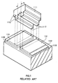
- FIGS. 1 and 2 show the disassembled construction of a conventional multi-beam laser.
- FIG. 1 shows a multi-beam laser with two laser beams.
- FIG. 2 shows a multi-beam laser with four laser beams.
- These multi-beam laser have the plurality of laser oscillators 110 on the same substrate 111.
- Each of those electrode 117 is electrically connected to each contact electrode 131 formed on a base 132 with each wiring 133 in between, respectively.
- Increase in the number of laser beams requires narrower space between each laser beam. For example, suppose the space between two laser beams is 60 ⁇ m. Then, if the number of laser beams are four, the space between each laser beam will be 20 ⁇ m. In this way, as the number of laser beams increases, the space S 1 between each laser oscillator 110 becomes narrower.
- each contact electrode 131 is connected to the whole surface of each electrode 117 on each laser oscillator 110, respectively. For that reason, when the number of the laser beams increases and the space S 1 between each laser oscillator 110 becomes narrower, extremely highly precise position matching has been required for those laser beams. That is, since each space between each electrode 117 and each contact electrode 131 are close, a small displacement of each contact electrode 131 makes one contact electrode 131 connect to the electrode 117 of two laser oscillators 110, respectively. Thus, each laser oscillator 110 can not be driven independently. Therefore, if the number of laser beams is increased to achieve more rapidity and higher performance, it causes difficulty in connecting each contact electrode 131 and each electrode 117 accurately. For that reason, mass production has been also difficult.
- the present invention has been realized in view of such problems. It is an object of this invention to provide a photoelectric conversion element which can keep easy and accurate connection of contact electrode and a method for manufacturing the same.
- the photoelectric conversion element comprises: a photoelectric conversion portion having a semiconductor layer equipped on a substrate and an electrode equipped on the semiconductor layer, a contact electrode electrically connected to the electrode of the photoelectric conversion portion, and an insulating layer formed between the contact electrode and the electrode of the photoelectric conversion portion and equipped with an opening for connecting them electrically.
- the method for manufacturing the photoelectric conversion element according to this invention includes: forming a photoelectric conversion portion having a semiconductor layer equipped on a substrate and an electrode equipped on the semiconductor layer, forming an insulating layer having an opening for the electrode of the photoelectric conversion portion, and forming a contact electrode electrically connected to the electrode of the photoelectric conversion portion through the opening of the insulating layer.
- the electrode of the photoelectric conversion portion and the contact electrode are electrically connected through the opening of the insulating layer.
- high precision is not required for the position matching of the electrode and the contact electrode, being connected easily and accurately.
- the photoelectric conversion portion having the semiconductor layer equipped on the substrate and the electrode is formed first. Then, the insulating layer with the opening for this electrode is formed. Following that, the contact electrode is formed which is electrically connected to the electrode of the photoelectric portion through the opening of this insulating layer.
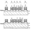
- FIG. 3 shows a whole structure of a laser diode that is a photo electric conversion element according to one embodiment of the invention.
- FIG. 4 shows a sectional structure taken on line II-II of FIG. 3.
- FIG.5 shows a structure disassembled along the line II-II of FIG. 2.
- a photoelectric conversion element refers to an element that converts optical energy and electric energy. This photoelectric conversion element converts optical energy to electric energy and vise versa.
- this laser diode has the plurality (4 in FIG. 3) of laser oscillator 10 as a photoelectric conversion portion deployed vertically to the resonator direction A.
- Each laser oscillator 10 may have the same structure each other. As shown in FIG. 4, n-type clad layer 12, active layer 13, p-type clad layer 14 and cap layer 15 are laminated successively on one surface, a surface (100), of the successive, same substrate 11.
- the size of each laser oscillator 10 may have the resonator direction A with 350 ⁇ m in length and with 12 ⁇ m in width in the vertical direction.
- a space S 1 between each laser oscillator 10 is, for example, 3 ⁇ m.
- a substrate 11 is composed of n-type GaAs with silicon, Si, or selenium, Se, as a n-type impurity, for example.
- Each n-type clad layer 12 is composed of n-type A1GaAs mixed crystal with silicon or selenium as a n-type impurity, for example.
- composition ratio in a class III chemical element of this n-type A1GaAs mixed crystal is, for example, 45% aluminum, A1, and 55% gallium (%: mole %.)
- Each active layer 13 is composed of, for example, i-A1GaAs mixed crystal without impurities ('i-' refers to no impurities.)
- the composition ratio in a class III chemical element of this n-type A1GaAs mixed crystal is, for example, 14% aluminum, A1, and 86% gallium.
- Each p-type clad layer 14 is composed of, for example, p-type A1GaAs mixed crystal with zinc, Zn, as a impurity.
- composition ratio in a class III chemical element of this p-type A1GaAs mixed crystal is, for example, 45% aluminum and 55% gallium.
- Each cap layer 15 is composed of, for example, p-type A1GaAs mixed crystal with zinc as a p-type impurity.
- Each p-type clad layer 14 has current block layers 16 inserted in both sides along the resonator direction A which is vertical to the surface of paper in FIG. 4 in part of the laminated layer direction. That is, each p-type clad layer 14 becomes narrower in width in the resonator direction A and in the vertical direction constructing a current narrowing portion.
- Each of these current block layers 16 is composed of, for example, n-type GaAs with silicon or selenium as a n-type impurity.
- Each laser oscillator 10 also has each p-side electrode 17 at the opposite side of the p-type clad layer 14 of each cap layer 15, respectively, while the other surface opposing to one surface of the substrate 11 has an n-side electrode 18, respectively.
- Each p-side electrode 17 has an alloy composition made by laminating a titanium (Ti) layer, a platinum (Pt) layer and a gold (Au) layer, for example, successively from the side of the cap layer 15 and heat is added thereon to be connected electrically to each cap layer 15.
- An n-side electrode 18 has an alloy composition made by laminating an alloy layer consisting of gold and germanium (Ge), a nickel (Ni) layer, and a gold (Au) layer, for example, successively from the side of the substrate 11 and heat is added thereon to be connected electrically to the substrate 11.
- each laser oscillator 10 has a pair of facing films 19a and 19b, respectively, which are placed successively each other on a pair of sides vertical to the resonator direction A.
- One facing film 19a is composed of oxide aluminum (A1 2 O 3 ), for example, and has a low reflection factor.
- Another facing film 19b is composed by laminating an oxide aluminum layer and an amorphous silicon layer alternately, for example, and has a high reflection factor. In other words, light occurred in each active layer 13 is amplified by traveling between a pair of facing films 19a and 19b to be injected as a laser beam from the facing film 19a , respectively.
- a mutually successive insulating layer 20 which is composed of an insulating material such as nitriding silicon (Si 3 N 4 ) is formed so as to cover each p-side electrode 17 on each laser oscillator 10. That is, this insulating layer 20 covers a pair of sides parallel with the resonator direction A of each of the laser oscillator 10, i.e. sides of each semiconductor layer and each p-side electrode 17, and the surface between each laser oscillator 10, respectively.
- the thickness of this insulating layer 20 is , for example, 0.15 ⁇ m and has the plurality of openings 21 corresponding to each p-side electrode 17.
- Each opening 21 exposes about half of one side in the resonator direction A among each p-side electrode 17 and is placed alternately not to be side by side in the arrangement direction B which is vertical to the resonator direction A between each laser oscillator 10 mutually placed side by side.
- FIG. 6 shows a sectional structure near a laser oscillator 10 taken on line II-II of FIG. 4.
- each area is divided in a grid by each line X drawn between each laser oscillator 10 in parallel with the resonator direction A and by each line Y drawn in the center of each laser oscillator 10 vertically to the resonator direction A.
- Each opening 21 is placed within each area which aligns in a slanting direction or aligns longitudinally or laterally with more than one area of space between the areas the openings are positioned.
- each opening 21 corresponding to each laser oscillator 10 placed side by side is placed within each area placed in a mutually slanting direction.
- the space S 2 between each opening 21 placed side by side in the alignment direction B has one laser oscillator 10 between each other, the space S 2 is opened wide enough as much as about 18 ⁇ m.
- the space S 3 between each opening 21 in the resonator direction A is opened widely enough as much as about 18 ⁇ m in view of a displacement while manufacturing.
- each of the contact electrode 31 is electrically connected to the p-side electrode 17 in each laser oscillator 10 through each opening 21, respectively.
- broken lines indicate each position where the insulating layer is in a contact with each contact electrode 31, and dotted areas indicate each position where each opening 21 is in a contact with.
- each contact electrode 31 extends from the center of laser oscillator 10 to the outside in parallel with the alignment direction B corresponding to each opening 21, respectively.
- each contact electrode 31 corresponding to each laser oscillator 10 placed in one side off the center of the alignment direction B is extended toward the one side while each contact electrode corresponding to each laser oscillator 10 in the other side is extended toward the other side.
- each contact electrode 31 it is preferable to form each contact electrode 31 by extending from the position corresponding to each opening 21 because it widens a contact area with a wire 33 and lowers its resistance.
- the space S 4 between each contact electrode 31 in the alignment direction B and the space S 5 in the resonator direction A are opened widely enough, respectively, matching each position of the openings 21.
- Each contact electrode 31 is formed on one surface of a base substrate 32 through each wire 33 and constructed by sequentially laminating a platinum layer and a soldered layer (an alloy layer of Pb and Sn), for example from the side of the base 32.
- the base 32 is constructed by aluminum nitride (AlN), for example.
- Each wire 33 is constructed by sequentially laminating a titan layer, a platinum layer and a gold layer from the side of the base substrate 32.
- An insulating film 34 consists of aluminum nitride is formed on the surface of each wiring 33 except on wire pad 33 a, for connecting wires.
- the semiconductor laser according to this embodiment is further equipped with a position matching portion 40 for connecting each p-side electrode 17 and each contact electrode 31 on each laser oscillator 10.
- the position matching portion 40 has two substrate side position matching portions 41 formed on one surface of the substrate 11 and two base substrate side position matching portion 42 formed on one surface of the base substrate 32.
- Each substrate side position matching portion 41 has a form of protrusion with extended parallely with the resonator direction A and is placed to catch each laser oscillator 10, respectively.
- Each substrate side position matching 41 has almost the same internal construction as the one of each laser oscillator 10 except that a current block layes is equipped all over in the p-type clad layer, and each surface is constructed by the insulating film 20, respectively.
- the opposite side of substrate 11 according to each of the substrate side position matching portion 41 is fixed in a contact with each contact electrode 31, respectively.
- the substrate side position matching portion 41 can support the connection of each p-side electrode 17 and each contact electrode 31 on each laser oscillator 10 and, furthermore, support each laser oscillator 10 supplementary.
- each side position matching portion 41 has each opening 22 on at least a part of the opposing surface to each contact electrode 31.
- Each base substrate side position matching portion 42 is constructed with two dents formed by rectangularly removing part of sides of the contact electrode 31 and the wiring 33, respectively, corresponding to each substrate side position matching portion 41.
- a semiconductor laser with such a construction is manufactured by following.
- FIG. 7A prepares the substrate 11 consisting of n-type GaAs mix crystal, for example.
- MOCVD Metal Organic Chemical Vapor Deposition
- the active layer 13 consisting of I-A1GaAs mix crystal
- the p-type clad layer 14 consisting of I-A1GaAs mix crystal sequentially on the side of one surface (100 surface) of the substrate 11.
- each p-side electrode 17 remains in order to correspond to only each laser oscillator forming area 51 and each position matching portion forming area 53, respectively.
- each p-side electrode 17 After respectively forming each p-side electrode 17, as shown in FIG. 8B, by following the RIE method, remove selectively part of the cap layer 15, the p-type clad layer 14, the current block layer 16, the active layer 13 and the n-type clad layer 12, respectively using each p-side electrode 17 as a mask. Accordingly the active layer 13, the p-type clad layer 14, and the cap layer 15 are separated respectively according to each laser oscillator forming area 51 and each position matching portion forming area 53. This separation is done using each p-side electrode 17 as a mask directly, so a lithography process is not required and precise separation can be achieved with fewer process. However, without using each p-side electrode 17 as a mask, it is possible to form a resist film on each p-side electrode 17 through a lithography process selectively and etch the resist film used as a mask by following the RIE method to separate them.
- each opening 21 corresponding to each laser oscillator forming area 51 is formed on the whole surface of one side of the substrate 11 including the p-side electrode 17.
- each opening 22 is not shown in the section view, so the position in the sectional direction is shown in broken lines.
- Each opening 21 not shown in the sectional view is also shown in broken lines.
- each opening 21 and 22 on the insulating layer 20 wrap the other surface side of the substrate 11 so that the thickness of the substrate 11 becomes 100 ⁇ m. This permits easy cleaver of the substrate 11, which is done in a process described later.
- each base substrate 32 consisting of aluminum nitride, for example.
- the base substrate 32 consisting of aluminum nitride, for example.
- form each wiring 33 so as to by extend toward the outside of each oscillator in parallel with the alignment direction B from the position corresponding to each opening 20, respectively.
- each base substrate position matching portion 42 consisting of rectangularly dented portion corresponding to each substrate side position matching portion 41 on part of the side of each wiring 33, respectively.
- each contact electrode 31 makes correspondence to each opening 21 of the insulating layer 20, respectively.
- each contact electrode 31 so as to extend toward the outside of each oscillator in parallel with the alignment direction B from the position corresponding to each opening 20, respectively.
- each base position matching portion 42 consisting of rectangularly dented portion corresponding to each wiring 33 that matches to each substrate side position matching portion 41 on part of the side of each contact electrode 31, respectively.
- CVD method for example, form the insulating film consisting of aluminum nitride on each wiring 33 except on wire pad 33a, respectively.
- each laser oscillator 10 and each contact electrode 31, respectively make each oscillator 10 contact with each contact electrode 31.
- easy and accurate position matching is performed.
- each contact electrode 31 and each p-side electrode 17 of each laser oscillator 10 electrically through each opening 21 on the insulating film 20 formed between them.
- the space S 2 and S 3 between each opening 21 on the insulating layer 20 and the space S 4 and S 5 between each contact electrode 31 are formed widely enough. Therefore, the high accuracy for their position matching is not required, and mutually corresponding each p-side electrode 17 and each contact electrode 31 can be connected easily and accurately.
- heat processing allows each p-side electrode 17 of each substrate side position matching portion 41 to be jointed with each contact electrode 31 through each opening 22, respectively. Therefore, the joint between each laser oscillator 10 and each contact electrode 31 can be supported more strongly. Accordingly, the semiconductor laser shown in FIG. 3 is formed.
- a predetermined voltage is applied to between each p-side electrode 17 and n-side electrode 18 through each contact electrode 31 at the point of the power-on to each wire pad portion 33a of each wiring 33 and each n-side electrode 18 of each laser oscillator 10. This permits current injection into each active layer 13 in each laser oscillator 10 and light emission occurs due to electron-hole recombination, respectively. Those light rays travel between a pair of the edge face films 19a and 19b to be amplified and rejected from the edge face film 19a to the outside.
- each contact electrode 31 and each p-side electrode 17 are connected through each opening 21 of the insulating layer 20, respectively.
- each opening 21 and each contact electrode 31 are formed widely enough. So, it does not require high accuracy for their positioning, and each of them is connected easily and accurately. It allows mutually independent drive for each laser oscillator 10.
- each contact electrode 31 and each p-side electrode 17 are connected through each opening 21 of the insulating layer 20, respectively. While, each opening 21 is placed within each area of the gird-divided area on the surface parallel to the substrate 11 which aligns in a slanting direction or aligns longitudinally or laterally with more than one area of space in between the areas each opening is positioned. Therefore, it does not require highly accurate position matching between each contact electrode 31 and each p-side electrode 17. Accordingly, it does not require high accuracy for their positioning, and each of them is connected easily and accurately. It allows mutually independent drive of each oscillator 10 and mass production of the laser diode.
- the substrate side position matching portion 41 is equipped on the substrate 11, while the base side position matching portion 42 is equipped on the base 32, corresponding to the substrate side position matching portion 41.
- the substrate side position matching portion 41 and the base side position matching portion 42 By using the substrate side position matching portion 41 and the base side position matching portion 42, the position of each contact electrode 31 and each laser oscillator 10 are matched easily and accurately.
- each of contact electrodes 31 and p-side electrodes 17 are connected easily and accurately.
- each substrate side position matching portion 41 is protruded and fixed to each contact electrode 31.
- it can support the junction of each laser oscillator 10 and each contact electrode 31, and, furthermore, support each laser oscillator 10.
- each substrate side position matching portion 41 is constructed almost as same construction as each laser oscillator 10 to form each p-side electrode 17, while each opening 22 is formed to be opposed to each contact electrode 31 on the insulating film 20.
- the joint between each p-side electrode 17 of each substrate side position matching portion 41 and each contact electrode 31 allows stronger joint between each laser oscillator 10 and each contact electrode 31.
- each p-side electrode 17 is etched as a mask. This permits highly accurate separation with less process and achieves simpler manufacturing steps and lower manufacturing costs. Also, it eliminates displacement between each p-side electrode 17 and each cap layer 15. This enhance accuracy of position matching between each contact electrode 31 and each laser oscillator 10. Thus, each contact electrode 31 and each p-side electrode 17 can be connected accurately.
- the present invention has been described in connection with the preferred embodiment thereof, it will be understood that it is not intended to limit the invention to that embodiment and can be modified differently.
- the embodiment specifically describes a semiconductor laser with four laser oscillators 10 on the same substrate 11.
- the present invention can be applicable widely irrespective of the number of the laser oscillator 10.
- each opening 21 on the insulating film 20 is determined depending on each area divided in a grid by each line X drawn between each laser oscillator 10 in parallel with the resonator direction A on the surface parallel with the substrate 11 and by each line Y drawn vertically to the resonator direction A in the center of each laser oscillator 10.
- the number of line Y drawn vertically to the resonator direction A can be plural depending on the number of laser oscillator 10.
- each opening 21 can be formed within each of the areas divided in a grid which aligns in a slanting direction or aligns longitudinally or laterally with more than one area of space in between the areas each opening is positioned, in accordance with each of the laser oscillator 10 irrespective of the number of the laser oscillator 10.
- each opening 21 corresponding to each laser oscillator 10 placed side by side must be placed within each area placed in a slanting direction mutually among each area divided in a grid.
- the slanting direction refers to a direction other than longitudinal and lateral directions, and angle is not related.
- each of contact electrodes 31 is extended respectively in parallel with the alignment direction B corresponding to each of the openings 21, the extention may be done vertical to the alignment direction B.
- each of contact electrodoes may be fromed according to the form of each of the openings 21.
- successive insulating layers 20 are formed between each p-side electrode 17 and each contact electrode 31.
- each of insulating layers 20 may be formed separately between each p-side electrode 17 and each contact electrode 31 making correspondence with each p-side electrode 17.
- each laser oscillator 10 materials composing each laser oscillator 10 are described specifically with examples. However, it is also applicable when each laser oscillator 10 is composed of other materials.
- the embodiment is also applicable to the clad layer composed of InP and the active layer composed of InGaAs. Alternatively, it is also applicable to each clad layer composed of A1GaInP and the active layer composed of GaInP.
- each laser oscillator 10 describes the construction of each laser oscillator 10 by referring one example.
- each laser oscillator 10 having other constructions may also be applied in the same manner.
- it is applicable to the one with a guide layer or the one with a substrate on which a p-type clad layer, an active layer and an n-type clad layer are laminated sequentially. Therefore, although the p-side electrode 17 is connected to the contact electrode 31 in the above-mentioned embodiment, the present invention is also applicable in the same manner when a contact electrode is connected to an n-side electrode.
- each p-side electrode 17 of each laser oscillator 10 is connected to each contact electrode 31 formed on the base substrate 32.
- the present invention is also applicable to the one in which each semiconductor layer, each electrode and each contact electrode are laminated sequentially on a substrate.
- the above-mentioned embodiment specifically describes the semiconductor laser with laser oscillator 10 as a photoelectric conversion portion.
- the present invention is widely applicable to a photoelectric conversion element with other photoelectric conversion portion which converts photo energy to electric energy or vise versa.
- it is applicable to other semiconductor light emitting elements such as light emitting diode, LED or semiconductor light receptive element such as a photo-detector.
- the above-mentioned embodiment specifically describes the case in which the MOCVD method is used for laminating a semiconductor layers on the substrate 11.
- other method such as the Molecular Beam Epitaxy; MBE, method can be used.
- MBE Molecular Beam Epitaxy
- the preferred embodiment specifically described the case in which the RIE method is used for selectively removing a semiconductor layer with p-side electrode 17 as a mask, other dry etching or wet etching can be used.
- an insulating layer is equipped between an electrode of a photoelectric portion and a contact electrode, and, the electrode and the contact electrode are connected electrically through the opening.
- a position matching portion is provided for connecting the electrode of the photoelectric conversion portion and the contact electrode.
- a part of a substrate side position matching portion is fixed to the contact electrode.
- connection between a laser oscillator and the contact electrode is supplemented and, furthermore, the laser oscillator can be supported supplementary.
- the connection between laser oscillator and the contact electrode can be supported more strongly.
- a photoelectric conversion element after a semiconductor layer is equipped with an electrode, it is removed selectively by using the electrode as a mask so that the photoelectric conversion portion can be formed accurately through fewer process. Accordingly simpler manufacturing processes and a decrease in the production cost can be achieved. Also, it enhances the accuracy of position matching between the photoelectric conversion portion and the contact electrode, and also the electrode and the contact electrode can be connected accurately.
Landscapes
- Physics & Mathematics (AREA)
- Condensed Matter Physics & Semiconductors (AREA)
- General Physics & Mathematics (AREA)
- Electromagnetism (AREA)
- Optics & Photonics (AREA)
- Semiconductor Lasers (AREA)
- Photovoltaic Devices (AREA)
Applications Claiming Priority (2)
| Application Number | Priority Date | Filing Date | Title |
|---|---|---|---|
| JP12652798A JP4189610B2 (ja) | 1998-05-08 | 1998-05-08 | 光電変換素子およびその製造方法 |
| JP12652798 | 1998-05-08 |
Publications (3)
| Publication Number | Publication Date |
|---|---|
| EP0955704A2 true EP0955704A2 (fr) | 1999-11-10 |
| EP0955704A3 EP0955704A3 (fr) | 2007-09-05 |
| EP0955704B1 EP0955704B1 (fr) | 2012-12-05 |
Family
ID=14937418
Family Applications (1)
| Application Number | Title | Priority Date | Filing Date |
|---|---|---|---|
| EP99108868A Expired - Lifetime EP0955704B1 (fr) | 1998-05-08 | 1999-05-04 | Dispositif de conversion d'énergie électrique en photons et son méthode de fabrication |
Country Status (3)
| Country | Link |
|---|---|
| US (2) | US6310381B1 (fr) |
| EP (1) | EP0955704B1 (fr) |
| JP (1) | JP4189610B2 (fr) |
Families Citing this family (18)
| Publication number | Priority date | Publication date | Assignee | Title |
|---|---|---|---|---|
| JP2001244540A (ja) * | 2000-02-29 | 2001-09-07 | Matsushita Electric Ind Co Ltd | 半導体レーザ |
| JP2002374029A (ja) * | 2001-06-15 | 2002-12-26 | Sony Corp | マルチビーム半導体レーザ素子 |
| US6768053B1 (en) * | 2002-01-09 | 2004-07-27 | Nanoset, Llc | Optical fiber assembly |
| US7612443B1 (en) * | 2003-09-04 | 2009-11-03 | University Of Notre Dame Du Lac | Inter-chip communication |
| JP4704703B2 (ja) * | 2004-07-07 | 2011-06-22 | 株式会社リコー | アレイ型半導体レーザ装置 |
| US7449354B2 (en) | 2006-01-05 | 2008-11-11 | Fairchild Semiconductor Corporation | Trench-gated FET for power device with active gate trenches and gate runner trench utilizing one-mask etch |
| US8174067B2 (en) * | 2008-12-08 | 2012-05-08 | Fairchild Semiconductor Corporation | Trench-based power semiconductor devices with increased breakdown voltage characteristics |
| US8304829B2 (en) | 2008-12-08 | 2012-11-06 | Fairchild Semiconductor Corporation | Trench-based power semiconductor devices with increased breakdown voltage characteristics |
| US8227855B2 (en) * | 2009-02-09 | 2012-07-24 | Fairchild Semiconductor Corporation | Semiconductor devices with stable and controlled avalanche characteristics and methods of fabricating the same |
| US8148749B2 (en) * | 2009-02-19 | 2012-04-03 | Fairchild Semiconductor Corporation | Trench-shielded semiconductor device |
| US8049276B2 (en) * | 2009-06-12 | 2011-11-01 | Fairchild Semiconductor Corporation | Reduced process sensitivity of electrode-semiconductor rectifiers |
| JP6080167B2 (ja) | 2010-10-01 | 2017-02-15 | アプライド マテリアルズ インコーポレイテッドApplied Materials,Incorporated | 薄膜トランジスタ用途に用いられる砒化ガリウムに基づく材料 |
| US9070387B1 (en) | 2013-08-23 | 2015-06-30 | Western Digital Technologies, Inc. | Integrated heat-assisted magnetic recording head/laser assembly |
| US9042048B1 (en) | 2014-09-30 | 2015-05-26 | Western Digital (Fremont), Llc | Laser-ignited reactive HAMR bonding |
| US9202478B1 (en) | 2015-02-10 | 2015-12-01 | Western Digital (Fremont), Llc | Method and structure for soldering a laser submount to a mounting face of a slider |
| US10139693B2 (en) * | 2015-06-19 | 2018-11-27 | International Business Machines Corporation | Synaptic electronic devices with electrochromic device |
| US11251134B2 (en) | 2017-05-26 | 2022-02-15 | Sharp Kabushiki Kaisha | Semiconductor module and method for manufacturing same |
| US20240275127A1 (en) * | 2021-06-11 | 2024-08-15 | Ams-Osram International Gmbh | Semiconductor chip and component |
Citations (3)
| Publication number | Priority date | Publication date | Assignee | Title |
|---|---|---|---|---|
| US4441187A (en) | 1980-07-31 | 1984-04-03 | Bouley Jean Claude | A semiconductor laser light source |
| US5474954A (en) | 1994-03-30 | 1995-12-12 | Samsung Electronics Co., Ltd. | Method of manufacturing semiconductor laser diode using self alignment |
| US5504768A (en) | 1992-12-22 | 1996-04-02 | Electronics And Telecommunications Research Institute | Semiconductor laser device and method for manufacturing the same |
Family Cites Families (13)
| Publication number | Priority date | Publication date | Assignee | Title |
|---|---|---|---|---|
| JPS5321275B2 (fr) * | 1972-03-13 | 1978-07-01 | ||
| JPS55153388A (en) * | 1979-05-18 | 1980-11-29 | Nec Corp | Semiconductor laser device for oscillating multiple wavelength |
| JPS63276279A (ja) * | 1987-05-08 | 1988-11-14 | Mitsubishi Electric Corp | 半導体装置 |
| JP2780981B2 (ja) * | 1988-06-27 | 1998-07-30 | 三菱電機株式会社 | 多点発光型半導体レーザ及びその製造方法 |
| JP3356816B2 (ja) * | 1992-03-24 | 2002-12-16 | セイコーインスツルメンツ株式会社 | 半導体光電気変換装置 |
| DE4229498A1 (de) * | 1992-09-04 | 1994-03-10 | Deutsche Aerospace | Festkörperlaser |
| US5360761A (en) * | 1993-05-07 | 1994-11-01 | Xerox Corporation | Method of fabricating closely spaced dual diode lasers |
| US5533042A (en) * | 1993-10-12 | 1996-07-02 | Fuji Xerox Co., Ltd. | Semiconductor laser device and driving method for the same as well as tracking servo system employing the same |
| JP3732551B2 (ja) * | 1995-05-15 | 2006-01-05 | 株式会社東芝 | 半導体装置の製造方法 |
| US5999269A (en) * | 1996-02-09 | 1999-12-07 | Gte Laboratories Incorporated | One-dimensional active alignment of optical or opto-electronic devices on a substrate |
| US5703394A (en) * | 1996-06-10 | 1997-12-30 | Motorola | Integrated electro-optical package |
| US6081020A (en) * | 1998-02-20 | 2000-06-27 | Lucent Technologies Inc. | Linear PIN photodiode |
| US5977571A (en) * | 1998-02-26 | 1999-11-02 | Lucent Technologies, Inc. | Low loss connecting arrangement for photodiodes |
-
1998
- 1998-05-08 JP JP12652798A patent/JP4189610B2/ja not_active Expired - Lifetime
-
1999
- 1999-05-04 EP EP99108868A patent/EP0955704B1/fr not_active Expired - Lifetime
- 1999-05-06 US US09/306,183 patent/US6310381B1/en not_active Expired - Lifetime
-
2001
- 2001-08-09 US US09/925,574 patent/US6548317B2/en not_active Expired - Lifetime
Patent Citations (3)
| Publication number | Priority date | Publication date | Assignee | Title |
|---|---|---|---|---|
| US4441187A (en) | 1980-07-31 | 1984-04-03 | Bouley Jean Claude | A semiconductor laser light source |
| US5504768A (en) | 1992-12-22 | 1996-04-02 | Electronics And Telecommunications Research Institute | Semiconductor laser device and method for manufacturing the same |
| US5474954A (en) | 1994-03-30 | 1995-12-12 | Samsung Electronics Co., Ltd. | Method of manufacturing semiconductor laser diode using self alignment |
Also Published As
| Publication number | Publication date |
|---|---|
| US20010049152A1 (en) | 2001-12-06 |
| JPH11330604A (ja) | 1999-11-30 |
| EP0955704B1 (fr) | 2012-12-05 |
| US6548317B2 (en) | 2003-04-15 |
| JP4189610B2 (ja) | 2008-12-03 |
| EP0955704A3 (fr) | 2007-09-05 |
| US6310381B1 (en) | 2001-10-30 |
Similar Documents
| Publication | Publication Date | Title |
|---|---|---|
| US6548317B2 (en) | Photoelectric conversion element and method for manufacturing the same | |
| EP0957548B1 (fr) | Réseau laser à longueurs d'onde multiples | |
| JP3748807B2 (ja) | 電気光学的特性が改善された半導体光放出装置及びその製造方法 | |
| JP4359345B2 (ja) | 不動態化垂直空洞面発光レーザ | |
| US7903709B2 (en) | Semiconductor laser device and method of manufacturing the same | |
| TW571448B (en) | Light-emitting diode array | |
| US20090262771A1 (en) | Semiconductor laser device and method of manufacturing the same | |
| US6567445B1 (en) | Method to manufacture a heat emission apparatus in a semiconductor laser | |
| US20110281382A1 (en) | Nitride-based semiconductor device and method of fabricating the same | |
| CN112152069A (zh) | 面发光激光器及其制造方法 | |
| US5642373A (en) | Monolithic semiconductor laser array of radially disposed lasers | |
| CN101656399B (zh) | 多束激光二极管 | |
| US6850547B2 (en) | Nitride based semiconductor laser device and method of fabricating the same | |
| JP2001015851A (ja) | 半導体レーザ素子及びその作製方法 | |
| US5802088A (en) | Stack type semiconductor laser device | |
| US6343087B2 (en) | Semiconductor laser | |
| JPH07111357A (ja) | 半導体レーザの製造方法 | |
| US12490540B2 (en) | Optical semiconductor array | |
| JP4816990B2 (ja) | 発光素子および半導体素子ならびにそれらの製造方法 | |
| EP1734623B1 (fr) | Laser à émission de surface avec élément de redressage integré | |
| WO1999008351A1 (fr) | Laser a semi-conducteur a emission par la surface et son procede de fabrication | |
| JPWO1999008351A1 (ja) | 面発光型半導体レーザ及びその製造方法 | |
| JP4081897B2 (ja) | 積層型半導体レーザ装置およびその製造方法 | |
| JPH04180677A (ja) | 半導体集積素子 | |
| JPS63204685A (ja) | 半導体レ−ザ素子およびその製造方法 |
Legal Events
| Date | Code | Title | Description |
|---|---|---|---|
| PUAI | Public reference made under article 153(3) epc to a published international application that has entered the european phase |
Free format text: ORIGINAL CODE: 0009012 |
|
| AK | Designated contracting states |
Kind code of ref document: A2 Designated state(s): AT BE CH CY DE DK ES FI FR GB GR IE IT LI LU MC NL PT SE |
|
| AX | Request for extension of the european patent |
Free format text: AL;LT;LV;MK;RO;SI |
|
| PUAL | Search report despatched |
Free format text: ORIGINAL CODE: 0009013 |
|
| AK | Designated contracting states |
Kind code of ref document: A3 Designated state(s): AT BE CH CY DE DK ES FI FR GB GR IE IT LI LU MC NL PT SE |
|
| AX | Request for extension of the european patent |
Extension state: AL LT LV MK RO SI |
|
| 17P | Request for examination filed |
Effective date: 20080130 |
|
| 17Q | First examination report despatched |
Effective date: 20080229 |
|
| AKX | Designation fees paid |
Designated state(s): DE FR GB |
|
| REG | Reference to a national code |
Ref country code: DE Ref legal event code: R079 Ref document number: 69944508 Country of ref document: DE Free format text: PREVIOUS MAIN CLASS: H01S0003025000 Ipc: H01L0033380000 |
|
| RIC1 | Information provided on ipc code assigned before grant |
Ipc: H01L 33/62 20100101ALI20120302BHEP Ipc: H01S 5/40 20060101ALI20120302BHEP Ipc: H01L 31/00 20060101ALI20120302BHEP Ipc: H01L 33/38 20100101AFI20120302BHEP |
|
| RTI1 | Title (correction) |
Free format text: CONVERSION ELEMENT CONVERTING ELECTRIC ENERGY TO PHOTONS AND METHOD FOR MANUFACTURING THE SAME |
|
| GRAP | Despatch of communication of intention to grant a patent |
Free format text: ORIGINAL CODE: EPIDOSNIGR1 |
|
| GRAS | Grant fee paid |
Free format text: ORIGINAL CODE: EPIDOSNIGR3 |
|
| RIN1 | Information on inventor provided before grant (corrected) |
Inventor name: TANIGUCHI, TAKEHIRO Inventor name: UENO, NORIKO Inventor name: NARUI, HIRONOBU Inventor name: OKANO, NOBUKATA |
|
| GRAA | (expected) grant |
Free format text: ORIGINAL CODE: 0009210 |
|
| AK | Designated contracting states |
Kind code of ref document: B1 Designated state(s): DE FR GB |
|
| RAP1 | Party data changed (applicant data changed or rights of an application transferred) |
Owner name: SONY CORPORATION |
|
| REG | Reference to a national code |
Ref country code: GB Ref legal event code: FG4D |
|
| REG | Reference to a national code |
Ref country code: DE Ref legal event code: R096 Ref document number: 69944508 Country of ref document: DE Effective date: 20130131 |
|
| PLBE | No opposition filed within time limit |
Free format text: ORIGINAL CODE: 0009261 |
|
| STAA | Information on the status of an ep patent application or granted ep patent |
Free format text: STATUS: NO OPPOSITION FILED WITHIN TIME LIMIT |
|
| 26N | No opposition filed |
Effective date: 20130906 |
|
| REG | Reference to a national code |
Ref country code: DE Ref legal event code: R097 Ref document number: 69944508 Country of ref document: DE Effective date: 20130906 |
|
| REG | Reference to a national code |
Ref country code: FR Ref legal event code: ST Effective date: 20140131 |
|
| PG25 | Lapsed in a contracting state [announced via postgrant information from national office to epo] |
Ref country code: FR Free format text: LAPSE BECAUSE OF NON-PAYMENT OF DUE FEES Effective date: 20130531 |
|
| REG | Reference to a national code |
Ref country code: DE Ref legal event code: R084 Ref document number: 69944508 Country of ref document: DE |
|
| REG | Reference to a national code |
Ref country code: GB Ref legal event code: 746 Effective date: 20150424 |
|
| REG | Reference to a national code |
Ref country code: DE Ref legal event code: R084 Ref document number: 69944508 Country of ref document: DE Effective date: 20150410 |
|
| PGFP | Annual fee paid to national office [announced via postgrant information from national office to epo] |
Ref country code: DE Payment date: 20180522 Year of fee payment: 20 |
|
| PGFP | Annual fee paid to national office [announced via postgrant information from national office to epo] |
Ref country code: GB Payment date: 20180518 Year of fee payment: 20 |
|
| REG | Reference to a national code |
Ref country code: DE Ref legal event code: R071 Ref document number: 69944508 Country of ref document: DE |
|
| REG | Reference to a national code |
Ref country code: GB Ref legal event code: PE20 Expiry date: 20190503 |
|
| PG25 | Lapsed in a contracting state [announced via postgrant information from national office to epo] |
Ref country code: GB Free format text: LAPSE BECAUSE OF EXPIRATION OF PROTECTION Effective date: 20190503 |