EP0957626B1 - Commutateur de batterie pour un circuit d'interface de ligne d'abonne' - Google Patents
Commutateur de batterie pour un circuit d'interface de ligne d'abonne' Download PDFInfo
- Publication number
- EP0957626B1 EP0957626B1 EP99109583A EP99109583A EP0957626B1 EP 0957626 B1 EP0957626 B1 EP 0957626B1 EP 99109583 A EP99109583 A EP 99109583A EP 99109583 A EP99109583 A EP 99109583A EP 0957626 B1 EP0957626 B1 EP 0957626B1
- Authority
- EP
- European Patent Office
- Prior art keywords
- subscriber loop
- interface circuit
- loop interface
- amplifiers
- power
- Prior art date
- Legal status (The legal status is an assumption and is not a legal conclusion. Google has not performed a legal analysis and makes no representation as to the accuracy of the status listed.)
- Expired - Lifetime
Links
- 238000000034 method Methods 0.000 claims description 13
- 230000004913 activation Effects 0.000 claims description 3
- 230000007704 transition Effects 0.000 description 4
- 238000010586 diagram Methods 0.000 description 2
- 238000005516 engineering process Methods 0.000 description 2
- 238000006243 chemical reaction Methods 0.000 description 1
- 230000008878 coupling Effects 0.000 description 1
- 238000010168 coupling process Methods 0.000 description 1
- 238000005859 coupling reaction Methods 0.000 description 1
- 230000007423 decrease Effects 0.000 description 1
- 230000003247 decreasing effect Effects 0.000 description 1
- 230000001419 dependent effect Effects 0.000 description 1
- 238000001514 detection method Methods 0.000 description 1
- 239000004065 semiconductor Substances 0.000 description 1
Images

Classifications
-
- H—ELECTRICITY
- H04—ELECTRIC COMMUNICATION TECHNIQUE
- H04Q—SELECTING
- H04Q1/00—Details of selecting apparatus or arrangements
- H04Q1/18—Electrical details
- H04Q1/28—Current-supply circuits or arrangements for selection equipment at exchanges
-
- H—ELECTRICITY
- H04—ELECTRIC COMMUNICATION TECHNIQUE
- H04M—TELEPHONIC COMMUNICATION
- H04M19/00—Current supply arrangements for telephone systems
- H04M19/001—Current supply source at the exchanger providing current to substations
- H04M19/005—Feeding arrangements without the use of line transformers
-
- Y—GENERAL TAGGING OF NEW TECHNOLOGICAL DEVELOPMENTS; GENERAL TAGGING OF CROSS-SECTIONAL TECHNOLOGIES SPANNING OVER SEVERAL SECTIONS OF THE IPC; TECHNICAL SUBJECTS COVERED BY FORMER USPC CROSS-REFERENCE ART COLLECTIONS [XRACs] AND DIGESTS
- Y02—TECHNOLOGIES OR APPLICATIONS FOR MITIGATION OR ADAPTATION AGAINST CLIMATE CHANGE
- Y02D—CLIMATE CHANGE MITIGATION TECHNOLOGIES IN INFORMATION AND COMMUNICATION TECHNOLOGIES [ICT], I.E. INFORMATION AND COMMUNICATION TECHNOLOGIES AIMING AT THE REDUCTION OF THEIR OWN ENERGY USE
- Y02D30/00—Reducing energy consumption in communication networks
- Y02D30/70—Reducing energy consumption in communication networks in wireless communication networks
Definitions
- This invention relates to semiconductor subscriber loop interface circuits (SLIC's) and, more specifically, relates to power management of subscriber loop interface circuits as mentioned in the pre-characterising portion of claim 1.
- SLIC's semiconductor subscriber loop interface circuits
- Telecommunication systems employ access products (e .g., remote terminals or subscriber interface units) for interfacing with each individual subscriber unit.
- An access product may include a SLIC for performing two to four wire conversion, battery feed, line supervision, and common-mode rejection. Together the SLIC, subscriber unit, and interface lines (e .g., TIP and RING lines) form a subscriber loop.
- the subscriber unit In a subscriber loop, the subscriber unit is generally powered from the SLIC through the interface lines. Typically, the SLIC must deliver 3 to 5 volts DC to a subscriber unit (e.g., a telephone) for off-hook states and deliver -42.5 to -56 volts DC (i.e., open circuit voltage levels) for on-hook states. SLIC's are generally powered with a -48 V power supply and are backed up with a power supply of the same magnitude.
- a SLIC may be of the type that applies a voltage signal to the TIP and RING lines in an asymmetrical manner as illustrated in Figure 1.
- the SLIC may hold the voltage signal on the TIP line essentially constant (e .g., -4 Volts) while varying the voltage signal on the RING line (e.g., -4 to -44 Volts) according to a predetermined relationship between loop current and the load resistance ( i . e ., resistance across TIP and RING).
- the predetermined relationship may be constant current or constant voltage through an internal source resistance, either physically defined or simulated via feedback.
- SLIC's When installed, SLIC's are coupled to loads of variable resistance.
- the resistance being primarily a function of loop length.
- the SLIC For short loop lengths (i.e., small resistance), the SLIC requires less than a conventional SLIC power supply to drive the subscriber loop.
- Excess power is dissipated in the output stages of line interface amplifiers on-board the SLIC. The power dissipation increases the SLIC operating temperature and decreases line interface reliability. Accordingly, the power management of SLIC's for widely variable loop lengths is a problem which has not been effectively solved since the inception of SLIC's over fifteen years ago.
- SLIC's are often installed in equipment that is located at a remote site not having access to a continuous power source. It is imperative for these technologies to have efficient and reliable SLIC operation.
- a SLIC is directly coupled to a conventional SLIC battery supply and coupled to second battery of the same magnitude through a discrete switch.
- a circuit detects loop voltage signals and compares loop voltage signals to an internal or external reference voltage.
- the circuit implementing this technique includes a loop voltage detect circuit, a comparator with hysteresis, two series high current bipolar devices (for switching), and an associated level shifter to operate the switches.
- the conventional SLIC power supply is replaced with a variable voltage power supply and complex switched mode power supply circuitry. In both techniques, the additional circuitry increases circuit complexity, size, density, operational temperature, and/or cost.
- US-A-5 737 411 discloses a telephone subscriber line interface circuit including a first circuit portion and a second circuit portion, a first battery voltage and a second battery input for receiving a second battery voltage.
- the second circuit portion is coupled to the second battery input.
- the telephone subscriber line interface circuit further includes a switch for coupling the first circuit portion to one of the first battery input and the second battery input.
- WO-A 96/15617 discloses an apparatus for automatically switching a load between different supply voltages in dependence on varying voltage demands of the load, which comprises a number of analog serious regulators.
- the supply voltage connection terminals of the serious regulators are to be connected to an individual one of that supply voltages, while the output terminals of the serious regulators are to be connected to the load to individually conduct current to/from the load in one and the same direction.
- An object of the present invention is to provide a method for efficiently powering a SLIC with a primary and a secondary voltage source, and to provide a novel SLIC having a circuit for reducing the power consumption of the SLIC, and also to provide a novel SLIC having a circuit for automatically powering a subscriber loop by steering current to a secondary power supply.
- Another object is to provide a SLIC having a circuit for varying the voltage of a secondary power supply as a function of the loop signals.
- the present invention includes a method of powering a subscriber loop interface circuit in supplying power to a subscriber loop comrising the steps of powering a subscriber loop interface circuit with a primary power supply; characterized by sensing the power requirements of said subscriber loop interface circuit; reducing the power consumption of said subscriber loop interface circuit as a function of sensed power requirements, in which step of reducing the power consumption comprises the steps of powering said subscriber loop interface circuit with a secondary power supply less than the primary power supply, wherein the subscriber loop interface circuit includes two line amplifiers and in that the step of reducing the power consumption includes the step of directing up to all the current away from the output terminal of one of said two amplifiers to said secondary power supply.
- the invention also includes a method as claimed in claim 3 wherein the step of powering the subscriber loop interface circuit includes the step of varying the voltage magnitude of said secondary power supply as a function of the sensed power requirements, and preferably the power requirement is sensed by determining the voltage across the TIP and RING lines of the subscriber loop, or the power requirement is sensed by determining the current in the subscriber loop.
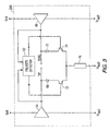
- Figure 2 refers to a SLIC 100 operating from a negative supply may include a TIP line amplifier 12, RING line amplifier 14, voltage regulator 16, and a diode 22.
- the type of SLIC 100 may be a voltage feed/current sense or a current feed/voltage sense.
- the type of amplifier 12 and 14 may be voltage follower or transconductance amplifiers.
- V bat1 e .g., -48 Volts
- V bat2 the voltage on the output terminal of the RING amplifier 14
- V d the drop across the diode 22
- V bat2 may be -24 Volts.
- the diode activation directs or steers current from the output of the amplifier 14 to the secondary power supply V bat2 through line 36 and resistive element 32.
- the current flowing in line 36 subtracts from the current flowing into the output stage of the RING amplifier 14.
- the point at which current flows in the diode is a function of diode parameters and the magnitude of the secondary power supply V bat2 .
- the secondary power supply V bat2 provides a second source of power for the SLIC in supplying power to the subscriber loop.
- the secondary power supply less than the primary supply helps to reduce SLIC power consumption.
- the secondary power supply may provide up to all of the power needed for the SLIC to drive the loop.
- the magnitude of the secondary supply V bat2 may be carefully selected to achieve minimum power consumption for a given loop length condition.
- the voltage controller 16 may generate a control signal V bat2-control on a terminal 34 for varying the magnitude of the secondary power supply V bat2 as a function of sensed loop current or voltage signals. Methods of sensing loop current or voltage signals are generally known in the art.
- the resistive element 32 may be a resistor, transistor, or equivalent.
- the transition of the current to path 36 is gradual and does not generate switching noise or sudden demands for power. Signal handling is impacted only slightly at the point of transition.
- the SLIC 100 may automatically transition to the primary voltage supply V bat1 .
- the automatic transition is inherent to the described circuit. If the loop voltage drops to zero, as it would in the on-hook condition, the diode 22 becomes reverse biased and V bat1 appears on the output terminal of the RING line amplifier 14 as controlled by one known SLIC line amplifier feedback technique.
- Whether the directing element i . e ., the diode 22 is coupled to the output terminal of the TIP line amplifier 12 or RING line amplifier 14 is dependent on the differential polarity of the TIP and RING lines and the polarity of the SLIC power supply. For a SLIC operating from a negative voltage, current from the output of the more negative amplifier is directed to the secondary power supply. For a SLIC operating from a positive voltage, current from the output of the more positive amplifier is directed to the secondary power supply.
- FIG. 3 shows a SLIC 200 of the type having polarity reversal of TIP and RING lines includes a polarity detector 62, TIP line amplifier 64, RING line amplifier 66, TIP line diode 68, RING line diode 70, TIP polarity transistor 72, and RING polarity transistor 74, and resistive element 76.
- the polarity detector 62 determines the differential polarity across the output terminals of the TIP and RING line amplifiers and provides a base current to the appropriate transistor 72 or 74.
- the polarity of the SLIC power supply dictates to which transistor the base current is provided. For a negative power supply, the base current is provided to the transistor coupled to the more negative output terminal. For a positive power supply, the base current is provided to the transistor coupled to the more positive output terminal.
- the transistor 72 or 74 conducts only if the corresponding diode 68 or 70 is forward biased.
- a base current flows to TIP polarity transistor 72.
- a base current flows to the TIP polarity transistor 72 and the TIP line diode 68 is forward biased, current flows in internal resistor 76 to V bat2 .
- a subscriber loop interface circuit includes a current directing element for directing current from the output stage of line interface amplifiers.
- the current is directed to a secondary power supply having a magnitude lower than the conventional primary power supply of a subscriber loop interface circuit in supplying power to a subscriber loop.
Landscapes
- Engineering & Computer Science (AREA)
- Power Engineering (AREA)
- Signal Processing (AREA)
- Computer Networks & Wireless Communication (AREA)
- Interface Circuits In Exchanges (AREA)
- Devices For Supply Of Signal Current (AREA)
Claims (9)
- Un procédé pour alimenter un circuit d'interface de ligne d'abonné (100) en énergie en fournissant de l'énergie à une ligne d'abonné, comprenant les étapes consistant à alimenter un circuit d'interface de ligne d'abonné (100) avec une source d'énergie primaire (Vbat1) en détectant les besoins en alimentation énergétique dudit circuit d'interface de ligne d'abonné ; réduire la consommation d'énergie dudit circuit d'interface de ligne d'abonné comme une fonction des besoins en alimentation énergétique détectés, laquelle étape de réduire la consommation d'énergie comprend les étapes d'alimenter ledit circuit d'interface de ligne d'abonné avec une source d'énergie secondaire (Vbat2) plus faible que la source d'énergie primaire (Vbat1), caractérisé en ce que le circuit d'interface de ligne d'abonné (100) comprend deux amplificateurs de ligne (12, 14) et en ce que l'étape de réduire la consommation d'énergie comprend l'étape de diriger jusqu'à la totalité de l'énergie électrique à l'écart de la borne de sortie de l'un desdits deux amplificateurs vers ladite source d'énergie secondaire (Vbat2).
- Un procédé selon la revendication 1, caractérisé par la dissipation de la puissance de l'énergie électrique dirigée à l'écart de la borne de sortie par l'écoulement de l'énergie électrique à travers un élément de résistance.
- Un procédé selon la revendication 2, dans lequel le circuit d'interface de ligne d'abonné (100) comprend deux amplificateurs de ligne (12, 14) et dans lequel les besoins en alimentation énergétique sont détectés et la consommation d'énergie est réduite en appliquant un potentiel aux bornes d'une diode (22) disposée en série entre la borne de sortie de l'un desdits deux amplificateurs de ligne (12, 14) et ladite source d'énergie secondaire (Vbat2), et dans lequel jusqu'à l'entièreté de l'énergie électrique est dirigée à l'écart en détectant le différentiel de polarité aux bornes de sortie desdits deux amplificateurs de ligne (12, 14), et en sélectionnant l'un desdits deux amplificateurs d'interface de ligne comme une fonction du différentiel de polarité détecté.
- Un procédé selon la revendication 3, dans lequel l'étape d'alimenter le circuit d'interface de ligne d'abonné (100) comprend l'étape de varier la valeur absolue de la tension de ladite source d'énergie secondaire (Vbat2) comme une fonction des besoins en alimentation énergétique détectés, et les besoins en alimentation énergétique sont détectés en déterminant la tension aux lignes TIP et RING de la ligne d'abonné, ou les besoins en alimentation énergétique sont détectés en déterminant l'énergie électrique dans la ligne d'abonné.
- Un circuit d'interface de ligne d'abonné du type possédant des besoins variables en alimentation énergétique, un dispositif pour détecter les besoins en alimentation énergétique et pour réduire l'énergie appliquée audit circuit d'interface de ligne d'abonné comme une fonction des besoins en alimentation énergétique détectés, dans lequel ledit circuit d'interface de ligne d'abonné comprend une borne d'énergie électrique primaire adaptée pour connexion avec une source d'énergie primaire (Vbat1), ledit dispositif comprend une borne d'énergie électrique secondaire adaptée pour connexion avec une source d'énergie secondaire (Vbat2) plus faible que la source d'énergie primaire (Vbat1), et ledit circuit d'interface de ligne d'abonné (100) devant être alimenté en énergie par la source d'énergie secondaire (Vbat2) à travers ladite borne d'énergie électrique secondaire pour réduire ainsi la consommation d'énergie dudit circuit d'interface de ligne d'abonné, caractérisé en ce que ledit circuit d'interface de ligne d'abonné comprend deux amplificateurs d'interface de ligne (12, 14), ledit dispositif comprend une diode (22) disposée en série entre la borne de sortie de l'un desdits deux amplificateurs de ligne et ladite source d'énergie secondaire pour détecter les besoins en alimentation énergétique et pour diriger jusqu'à la totalité de l'énergie électrique à l'écart de la borne de sortie dudit l'un desdits deux amplificateurs de ligne (12, 14) vers ladite source d'énergie secondaire (Vbat2).
- Un circuit d'interface de ligne d'abonné selon la revendication 5, comprenant un dispositif de dissipation pour dissiper la puissance de l'énergie électrique dirigée à l'écart de ladite borne de sortie, et ledit dispositif de dissipation comprend un élément de résistance (32) répondant à ladite diode pour dissiper la puissance.
- Un circuit d'interface de ligne d'abonné selon la revendication 6, dans lequel ledit circuit d'interface de ligne d'abonné comprend deux amplificateurs d'interface de ligne (12, 14) et ledit dispositif comprend des moyens de détection de polarité pour détecter le différentiel de polarité aux bornes de sortie desdits deux amplificateurs d'interface de ligne, des moyens de sélection répondant auxdits moyens de détection de polarité pour sélectionner la borne de sortie de l'un desdits deux amplificateurs d'interface ligne comme une fonction du différentiel de polarité détecté, et des moyens de direction répondant auxdits moyens de sélection pour diriger jusqu'à l'entièreté de l'énergie électrique à l'écart de la borne de sortie sélectionnée vers la source d'énergie secondaire, dans lequel les moyens de direction comprennent une diode (22) disposée en série entre la borne de sortie de chacun desdits deux amplificateurs d'interface de ligne et ladite borne d'énergie électrique secondaire.
- Un circuit d'interface de ligne d'abonné selon les revendications 6 ou 7, dans lequel ledit dispositif comprend des moyens de déclenchement répondant aux signaux de tension sur ladite borne d'énergie électrique secondaire et répondant aux signaux de tension sur la borne de sortie de l'un desdits deux amplificateurs d'interface de ligne pour diriger l'énergie électrique à l'écart de la borne de sortie dudit l'un desdits deux amplificateurs d'interface ligne (12, 14) vers ladite source d'énergie secondaire (Vbat2), de manière à réduire la consommation d'énergie dudit circuit d'interface de ligne d'abonné, lesdits moyens de déclenchement comprennent une diode (22) disposée en série entre la borne de sortie dudit l'un desdits deux amplificateurs d'interface ligne (12, 14) et ladite borne d'énergie électrique secondaire (Vbat2), et comprennent un dispositif de commande pour commander la valeur absolue de la tension de la source d'énergie secondaire externe comme une fonction des besoins en alimentation énergétique détectés.
- Un circuit d'interface de ligne d'abonné selon la revendication 8, dans lequel ledit circuit d'interface de ligne d'abonné comprend une paire de bornes adaptées pour connexion à des signaux d'abonné afin de former une ligne d'abonné à alimenter en énergie par ledit circuit d'interface de ligne d'abonné, ledit dispositif comprend des moyens pour mesurer la tension (16) afin de mesurer la tension aux bornes de ladite paire de bornes, détectant ainsi les besoins en alimentation énergétique dudit circuit d'interface de ligne d'abonné, ledit circuit d'interface de ligne d'abonné comprend une paire de bornes adaptées pour connexion à des signaux d'abonné afin de former une ligne d'abonné à alimenter en énergie par ledit circuit d'interface de ligne d'abonné ; et ledit dispositif comprend des moyens de détection d'énergie électrique pour détecter l'énergie électrique dans la ligne d'abonné, détectant ainsi les besoins en alimentation énergétique dudit circuit d'interface de ligne d'abonné.
Applications Claiming Priority (2)
| Application Number | Priority Date | Filing Date | Title |
|---|---|---|---|
| US79304 | 1998-05-15 | ||
| US09/079,304 US6233335B1 (en) | 1998-05-15 | 1998-05-15 | Battery switching subscriber loop interface circuit |
Publications (3)
| Publication Number | Publication Date |
|---|---|
| EP0957626A2 EP0957626A2 (fr) | 1999-11-17 |
| EP0957626A3 EP0957626A3 (fr) | 2003-03-05 |
| EP0957626B1 true EP0957626B1 (fr) | 2006-08-09 |
Family
ID=22149681
Family Applications (1)
| Application Number | Title | Priority Date | Filing Date |
|---|---|---|---|
| EP99109583A Expired - Lifetime EP0957626B1 (fr) | 1998-05-15 | 1999-05-14 | Commutateur de batterie pour un circuit d'interface de ligne d'abonne' |
Country Status (5)
| Country | Link |
|---|---|
| US (1) | US6233335B1 (fr) |
| EP (1) | EP0957626B1 (fr) |
| JP (1) | JP2000078622A (fr) |
| KR (1) | KR19990088319A (fr) |
| DE (1) | DE69932667T2 (fr) |
Families Citing this family (12)
| Publication number | Priority date | Publication date | Assignee | Title |
|---|---|---|---|---|
| SE512170C2 (sv) * | 1998-06-02 | 2000-02-07 | Ericsson Telefon Ab L M | Förfarande och anordning för val av matningsspänning |
| SE514853C2 (sv) * | 1999-10-04 | 2001-05-07 | Ericsson Telefon Ab L M | Anordning i en abonnentlinjekrets |
| SE0002350L (sv) * | 2000-06-21 | 2001-12-22 | Ericsson Telefon Ab L M | En metod att generera en ringsignal i en abonnentlinjekrets |
| SE520306C2 (sv) | 2001-01-31 | 2003-06-24 | Ericsson Telefon Ab L M | Regulator för en halvledarkrets |
| CA2360117A1 (fr) * | 2001-10-24 | 2003-04-24 | Catena Networks Canada Inc. | Utilisation de signaux de sonnerie de service telephonique de base sans perturbation des signaux de ligne d'acces numerique |
| US6947554B2 (en) * | 2001-11-08 | 2005-09-20 | Motorola, Inc. | Least mean power consumption in telecommunications systems |
| CA2411622A1 (fr) * | 2002-11-12 | 2004-05-12 | Catena Networks Canada Inc. | Sonnerie silencieuse avec dispositifs aux dimensions reduites |
| US20040120512A1 (en) * | 2002-12-20 | 2004-06-24 | Ploumen Franciscus Maria | System and method for optimizing power dissipation in subscriber interface line circuits (SLICS) |
| US20040151304A1 (en) * | 2003-02-05 | 2004-08-05 | George Scott A. | Method of managing power for devices requiring supply levels varying in accordance with operational state |
| US6956945B2 (en) * | 2003-03-07 | 2005-10-18 | Legerity, Inc. | Method and apparatus for phantom battery feed |
| CA2552706A1 (fr) | 2003-12-29 | 2005-07-28 | Grape Technology Group, Inc | Systeme et procede de traitement et de routage d'appels entrants pour systeme d'assistance a la communication |
| EP2638691B1 (fr) * | 2010-11-09 | 2015-07-15 | Telefonaktiebolaget L M Ericsson (Publ) | Système de distribution d'énergie à des lignes d'abonnés |
Family Cites Families (9)
| Publication number | Priority date | Publication date | Assignee | Title |
|---|---|---|---|---|
| US5511118A (en) * | 1991-01-31 | 1996-04-23 | Northern Telecom Limited | Method of providing d.c. feed to a telephone line |
| US5619567A (en) * | 1994-10-31 | 1997-04-08 | Advanced Micro Devices | Variable DC feed characteristic in a subscriber line interface circuit |
| SE503646C2 (sv) * | 1994-11-10 | 1996-07-22 | Ericsson Telefon Ab L M | Automatisk omkopplingsanordning |
| US5737411A (en) * | 1994-12-29 | 1998-04-07 | Advanced Micro Devices Inc. | Battery switching in a telephone subscriber line interface circuit |
| GB2304254B (en) * | 1995-08-04 | 1999-12-08 | Nokia Telecommunications Oy | Power supply for telecommunications devices |
| US5659608A (en) * | 1995-12-15 | 1997-08-19 | Lucent Technologies Inc. | Line feed circuit with logic level controlled ringing |
| US5721774A (en) * | 1995-12-15 | 1998-02-24 | Lucent Technologies Inc. | Longitudinally balanced, dual voltage line-feed circuit |
| US5881129A (en) * | 1996-05-10 | 1999-03-09 | Chen; Robert Kuo-Wei | Self-monitoring line interface circuit |
| US5854839A (en) * | 1996-05-10 | 1998-12-29 | Lucent Technologies Inc. | Dual voltage, self-monitoring line circuit |
-
1998
- 1998-05-15 US US09/079,304 patent/US6233335B1/en not_active Expired - Lifetime
-
1999
- 1999-05-14 EP EP99109583A patent/EP0957626B1/fr not_active Expired - Lifetime
- 1999-05-14 JP JP11134220A patent/JP2000078622A/ja active Pending
- 1999-05-14 DE DE69932667T patent/DE69932667T2/de not_active Expired - Lifetime
- 1999-05-15 KR KR1019990017477A patent/KR19990088319A/ko not_active Ceased
Also Published As
| Publication number | Publication date |
|---|---|
| JP2000078622A (ja) | 2000-03-14 |
| US6233335B1 (en) | 2001-05-15 |
| KR19990088319A (ko) | 1999-12-27 |
| EP0957626A2 (fr) | 1999-11-17 |
| EP0957626A3 (fr) | 2003-03-05 |
| DE69932667D1 (de) | 2006-09-21 |
| DE69932667T2 (de) | 2007-08-09 |
Similar Documents
| Publication | Publication Date | Title |
|---|---|---|
| US5737411A (en) | Battery switching in a telephone subscriber line interface circuit | |
| EP0615375B1 (fr) | Circuit d'interface de ligne d'abonné | |
| EP0957626B1 (fr) | Commutateur de batterie pour un circuit d'interface de ligne d'abonne' | |
| EP0435460B1 (fr) | Commande de répartition du courant pour des convertisseurs en parallèle | |
| US5721774A (en) | Longitudinally balanced, dual voltage line-feed circuit | |
| US6744151B2 (en) | Multi-channel power supply selector | |
| WO1994023489A1 (fr) | Circuit ameliore de couplage/decouplage de signaux a partage de courant pour systemes convertisseurs de puissance | |
| EP1705787B1 (fr) | Circuit d'équilibrage de courant | |
| US6229291B1 (en) | Current sharing control system of power supply and output voltage sensing circuit | |
| US5479329A (en) | Switching power supply having output terminal disconnection detecting circuit | |
| US5850137A (en) | Charging apparatus and current/voltage detector for use therein | |
| KR100391886B1 (ko) | 공급전압스위칭장치 | |
| EP0204978B1 (fr) | Dispositif de commande pour la mise hors service d'une source d'alimentation électrique | |
| US4677537A (en) | Converter device | |
| US4571460A (en) | Active impedance line feed circuit with improved ground fault protection | |
| US4423292A (en) | Detector circuit for communication lines | |
| US4631362A (en) | Low resistance origination scan circuit | |
| EP0155074B1 (fr) | Circuit d'alimentation de ligne à impédance active avec une protection contre les défauts de mise à terre | |
| KR100571016B1 (ko) | 가입자 회선 인터페이스 회로의 장치 | |
| JP3051275B2 (ja) | 加入者回路の給電方式 | |
| US6239648B1 (en) | System and method for dissipating heat in an electric device | |
| JPH0324384A (ja) | 電磁弁制御装置 | |
| JPH02143672A (ja) | 給電回路 | |
| WO1984004007A1 (fr) | Circuit de commande pour un moteur | |
| JPH01220945A (ja) | 加入者線状態監視回路 |
Legal Events
| Date | Code | Title | Description |
|---|---|---|---|
| PUAI | Public reference made under article 153(3) epc to a published international application that has entered the european phase |
Free format text: ORIGINAL CODE: 0009012 |
|
| AK | Designated contracting states |
Kind code of ref document: A2 Designated state(s): AT BE CH CY DE DK ES FI FR GB GR IE IT LI LU MC NL PT SE |
|
| AX | Request for extension of the european patent |
Free format text: AL;LT;LV;MK;RO;SI |
|
| PUAL | Search report despatched |
Free format text: ORIGINAL CODE: 0009013 |
|
| AK | Designated contracting states |
Kind code of ref document: A3 Designated state(s): AT BE CH CY DE DK ES FI FR GB GR IE IT LI LU MC NL PT SE Designated state(s): AT BE CH CY DE DK ES FI FR GB GR IE IT LI LU MC NL PT SE |
|
| AX | Request for extension of the european patent |
Extension state: AL LT LV MK RO SI |
|
| 17P | Request for examination filed |
Effective date: 20030726 |
|
| AKX | Designation fees paid |
Designated state(s): CH DE FR GB IT LI SE |
|
| 17Q | First examination report despatched |
Effective date: 20050513 |
|
| GRAP | Despatch of communication of intention to grant a patent |
Free format text: ORIGINAL CODE: EPIDOSNIGR1 |
|
| GRAC | Information related to communication of intention to grant a patent modified |
Free format text: ORIGINAL CODE: EPIDOSCIGR1 |
|
| GRAS | Grant fee paid |
Free format text: ORIGINAL CODE: EPIDOSNIGR3 |
|
| GRAA | (expected) grant |
Free format text: ORIGINAL CODE: 0009210 |
|
| AK | Designated contracting states |
Kind code of ref document: B1 Designated state(s): CH DE FR GB IT LI SE |
|
| PG25 | Lapsed in a contracting state [announced via postgrant information from national office to epo] |
Ref country code: LI Free format text: LAPSE BECAUSE OF FAILURE TO SUBMIT A TRANSLATION OF THE DESCRIPTION OR TO PAY THE FEE WITHIN THE PRESCRIBED TIME-LIMIT Effective date: 20060809 Ref country code: IT Free format text: LAPSE BECAUSE OF FAILURE TO SUBMIT A TRANSLATION OF THE DESCRIPTION OR TO PAY THE FEE WITHIN THE PRESCRIBED TIME-LIMIT;WARNING: LAPSES OF ITALIAN PATENTS WITH EFFECTIVE DATE BEFORE 2007 MAY HAVE OCCURRED AT ANY TIME BEFORE 2007. THE CORRECT EFFECTIVE DATE MAY BE DIFFERENT FROM THE ONE RECORDED. Effective date: 20060809 Ref country code: CH Free format text: LAPSE BECAUSE OF FAILURE TO SUBMIT A TRANSLATION OF THE DESCRIPTION OR TO PAY THE FEE WITHIN THE PRESCRIBED TIME-LIMIT Effective date: 20060809 |
|
| REG | Reference to a national code |
Ref country code: GB Ref legal event code: FG4D |
|
| REG | Reference to a national code |
Ref country code: CH Ref legal event code: EP |
|
| REF | Corresponds to: |
Ref document number: 69932667 Country of ref document: DE Date of ref document: 20060921 Kind code of ref document: P |
|
| PG25 | Lapsed in a contracting state [announced via postgrant information from national office to epo] |
Ref country code: SE Free format text: LAPSE BECAUSE OF FAILURE TO SUBMIT A TRANSLATION OF THE DESCRIPTION OR TO PAY THE FEE WITHIN THE PRESCRIBED TIME-LIMIT Effective date: 20061109 |
|
| REG | Reference to a national code |
Ref country code: CH Ref legal event code: PL |
|
| EN | Fr: translation not filed | ||
| PLBE | No opposition filed within time limit |
Free format text: ORIGINAL CODE: 0009261 |
|
| STAA | Information on the status of an ep patent application or granted ep patent |
Free format text: STATUS: NO OPPOSITION FILED WITHIN TIME LIMIT |
|
| 26N | No opposition filed |
Effective date: 20070510 |
|
| GBPC | Gb: european patent ceased through non-payment of renewal fee |
Effective date: 20070514 |
|
| PG25 | Lapsed in a contracting state [announced via postgrant information from national office to epo] |
Ref country code: FR Free format text: LAPSE BECAUSE OF FAILURE TO SUBMIT A TRANSLATION OF THE DESCRIPTION OR TO PAY THE FEE WITHIN THE PRESCRIBED TIME-LIMIT Effective date: 20070511 |
|
| PG25 | Lapsed in a contracting state [announced via postgrant information from national office to epo] |
Ref country code: GB Free format text: LAPSE BECAUSE OF NON-PAYMENT OF DUE FEES Effective date: 20070514 |
|
| PG25 | Lapsed in a contracting state [announced via postgrant information from national office to epo] |
Ref country code: FR Free format text: LAPSE BECAUSE OF FAILURE TO SUBMIT A TRANSLATION OF THE DESCRIPTION OR TO PAY THE FEE WITHIN THE PRESCRIBED TIME-LIMIT Effective date: 20060809 |
|
| PGFP | Annual fee paid to national office [announced via postgrant information from national office to epo] |
Ref country code: DE Payment date: 20130530 Year of fee payment: 15 |
|
| REG | Reference to a national code |
Ref country code: DE Ref legal event code: R119 Ref document number: 69932667 Country of ref document: DE |
|
| REG | Reference to a national code |
Ref country code: DE Ref legal event code: R119 Ref document number: 69932667 Country of ref document: DE Effective date: 20141202 |
|
| PG25 | Lapsed in a contracting state [announced via postgrant information from national office to epo] |
Ref country code: DE Free format text: LAPSE BECAUSE OF NON-PAYMENT OF DUE FEES Effective date: 20141202 |