EP0957634A2 - Caméra à bord - Google Patents
Caméra à bord Download PDFInfo
- Publication number
- EP0957634A2 EP0957634A2 EP99303730A EP99303730A EP0957634A2 EP 0957634 A2 EP0957634 A2 EP 0957634A2 EP 99303730 A EP99303730 A EP 99303730A EP 99303730 A EP99303730 A EP 99303730A EP 0957634 A2 EP0957634 A2 EP 0957634A2
- Authority
- EP
- European Patent Office
- Prior art keywords
- image pickup
- range
- normally
- pickup surface
- electronic signals
- Prior art date
- Legal status (The legal status is an assumption and is not a legal conclusion. Google has not performed a legal analysis and makes no representation as to the accuracy of the status listed.)
- Withdrawn
Links
- 230000003287 optical effect Effects 0.000 claims abstract description 32
- 238000003384 imaging method Methods 0.000 claims abstract description 17
- 238000000034 method Methods 0.000 claims abstract description 3
- 238000006243 chemical reaction Methods 0.000 description 13
- 230000000903 blocking effect Effects 0.000 description 3
- 239000002131 composite material Substances 0.000 description 2
- 238000010586 diagram Methods 0.000 description 2
- 230000000694 effects Effects 0.000 description 1
- 230000000873 masking effect Effects 0.000 description 1
- 239000000203 mixture Substances 0.000 description 1
- 230000002194 synthesizing effect Effects 0.000 description 1
Images
Classifications
-
- H—ELECTRICITY
- H04—ELECTRIC COMMUNICATION TECHNIQUE
- H04N—PICTORIAL COMMUNICATION, e.g. TELEVISION
- H04N25/00—Circuitry of solid-state image sensors [SSIS]; Control thereof
- H04N25/60—Noise processing, e.g. detecting, correcting, reducing or removing noise
- H04N25/62—Detection or reduction of noise due to excess charges produced by the exposure, e.g. smear, blooming, ghost image, crosstalk or leakage between pixels
- H04N25/625—Detection or reduction of noise due to excess charges produced by the exposure, e.g. smear, blooming, ghost image, crosstalk or leakage between pixels for the control of smear
-
- H—ELECTRICITY
- H04—ELECTRIC COMMUNICATION TECHNIQUE
- H04N—PICTORIAL COMMUNICATION, e.g. TELEVISION
- H04N25/00—Circuitry of solid-state image sensors [SSIS]; Control thereof
- H04N25/70—SSIS architectures; Circuits associated therewith
- H04N25/71—Charge-coupled device [CCD] sensors; Charge-transfer registers specially adapted for CCD sensors
- H04N25/73—Charge-coupled device [CCD] sensors; Charge-transfer registers specially adapted for CCD sensors using interline transfer [IT]
Definitions
- the present invention relates to an onboard camera including an image pickup element which photoelectrically converts light having passed through an optical system to store signal electric charges, and outputs the stored signal electric charges through a vertical transfer path and a horizontal transfer path.
- an image pickup element for converting an optically formed image of an object into an electric signal there is generally adopted an image pickup element such as a CCD element in which light is converted into electric signals at a photoelectric conversion portion, and stored signal electric charges are read out from a vertical transfer path through a horizontal transfer path.
- an interline transfer system CCD element in which a photoelectric conversion portion and a vertical transfer path are arranged to be two-dimensionally adjacent to each other, has come into wide use.
- the interline transfer system CCD element when an image of a highly bright object is taken, a white line appearing on a picture in a vertical scanning direction, a so-called smear occurs, which becomes a cause of erroneous recognition in picture recognition processing or the like.
- this smear occurs because electric charges overflowed by intense light at the photoelectric conversion portion enter the vertical transfer path, and smear resistance can be improved by using, for example, a frame interline transfer system CCD element provided with a memory region for storing signal electric charges below the vertical transfer path.
- the frame interline transfer system CCD element is used mainly in a field in which high picture quality is required, for example, for broadcasting, and is very expensive.
- the present invention has been made in view of the above circumstances, and an object is to provide an onboard camera capable of obtaining a picture with little influence of a smear by using a generally used inexpensive image pickup element which has an image pickup surface on which a photoelectric conversion portion for photoelectrically converting light having passed through an optical system to store signal electric charges, and a vertical transfer path for transferring the signal electric charges stored in the photoelectric conversion portion are arranged to be two-dimensionally adjacent to each other, and outputs the signal electric charges transferred to the vertical transfer path through a horizontal transfer path.
- an onboard camera comprising a built-in image pickup.
- element which has an image pickup surface on which a photoelectric conversion portion for photoelectrically converting light having passed through an optical system to store signal electric charges, and a vertical transfer path for transferring the signal electric charges stored in the photoelectric conversion portion are arranged to be two-dimensionally adjacent to each other, and outputs the signal electric charges transferred to the vertical transfer path through a horizontal transfer path, wherein the image pickup surface of the image pickup element is divided and set into two regions of a use region and a nonuse region in an up-and-down direction with respect to the vertical transfer path, and the image pickup element is disposed to be offset with respect to an imaging range of the optical system so that the use region is positioned within the imaging range of the optical system and the nonuse region is positioned outside of the imaging range of the optical system and at a head side.
- a member for blocking off incident light onto the nonuse region is disposed between the optical system and the image pickup element.
- the onboard camera of the invention preferably includes means for sheltering the signal electric charges stored in the use region through the vertical transfer path into the nonuse region at high speed just before or after exposure timing to the image pickup element.
- the member for blocking off the incident light onto the nonuse region between the optical system and the image pickup element it is preferable to shelter the signal electric charges stored in the use region through the vertical transfer path into the nonuse region at high speed just before or after the exposure timing to the image pickup element.
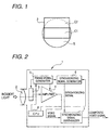
- Fig. 1 relates to a first embodiment of the present invention, and is an explanatory view showing an arrangement of a CCD element with respect to an imaging range of an optical image.
- Fig. 2 relates to a first embodiment of the present invention, and is a structural view of a camera.
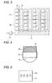
- Fig. 3 relates to a first embodiment of the present invention, and is a block diagram showing a structure of the CCD element.
- Fig. 4 relates to a second embodiment of the present invention, and is an explanatory view showing a light-shielding range to the CCD element.
- Fig. 5 relates to a second embodiment of the present invention, and is an explanatory view showing sheltering of signal electric charges of the CCD element into a nonuse region.
- Figs. 1 to 3 relates to a first embodiment of the invention
- Fig. 1 is an explanatory view showing an arrangement of a CCD element with respect to an imaging range of an optical image
- Fig. 2 is a structural view of a camera
- Fig. 3 is a block diagram showing a structure of the CCD element.
- reference numeral 1 denotes a camera which is mounted on a vehicle such as an automobile and takes a view outside of the vehicle to recognize a lane/road shape, an obstacle, and the like by picture recognition.
- This camera 1 is equipped with a CCD element 3 as an image pickup element for converting an image formed by an optical system 2 made of a lens group into an electric signal, an amplifier 4 for amplifying the signal from the CCD element 3, a timing signal generator 5 for generating timing signals to control the CCD element 3 and the amplifier 4, a synchronizing signal generator 6 for generating synchronizing signals (horizontal synchronizing signal and vertical synchronizing signal), a synchronizing signal synthesizer 7 for outputting a composite video signal (video signal) obtained by synthesizing a video signal outputted from the amplifier 4 and the synchronizing signals, a CPU 8 for collectively controlling circuits such as the timing signal generator 5 and the synchronizing signal generator 6 to make exposure control of the CCD element 3, and the like.
- the foregoing CCD element 3 is a well-known interline transfer system CCD element which is constituted by, as shown in Fig. 3, photodiodes 10 two-dimensionally arranged in the horizontal , direction and the vertical direction as photoelectric conversion portions for storing electric charges by receiving light, vertical shift registers 12 forming vertical transfer paths for sequentially transferring the electric charges stored in the photodiodes 10 by receiving light in the vertical direction through transfer gates 11, a horizontal shift register 13 forming a horizontal transfer path for sequentially transferring the electric charges transferred by the vertical shift registers 12 in the horizontal direction, an amplifier 14 for amplifying an output signal from the horizontal shift register 13 and outputting, and the like.
- the image pickup surface of the CCD element 3 can be divided into two regions C1 and C2 with reference to the upper region and lower region of the vertical shift register 12 as schematically indicated by broken lines in Fig. 3.
- a picture range in the vertical direction which is actually required is about one half of the whole image pickup surface.
- the one region C1 of the image pickup surface of the CCD element 3 is made a region which is used for normal picture recognition
- the other region C2 is made a region which is not normally used
- the CCD element 3 is disposed to be offset with respect to an imaging range R of the optical system 2 so that the use region C1 of the image pickup surface of the CCD element 3 is positioned within the imaging range R of the optical system 2 and the nonuse region C2 is positioned outside of the optical system 2 and at the head side.
- the upper and lower relation of the use region C1 and the nonuse region C2 may be opposite to the positional relation in Fig. 3.
- a pulse for controlling a signal electric charge storage period to the photodiode 10 a pulse for driving the vertical shift register 12, and a pulse for driving the horizontal shift register 13 are supplied from the timing signal generator 5 to the CCD element 3, and imaging light is changed into signal electric charges which are read out in, for example, a field storage mode.
- the video signal from the CCD element 3 is amplified by the amplifier 4, it is synthesized with the horizontal synchronizing signal and the vertical synchronizing signal from the synchronizing signal generator 6 so that the composite video signal is generated and is outputted to a not-shown picture processing device.
- the oblong picture generated on the image pickup surface of the use region C1 of the CCD element 3 becomes the picture in which influence of a smear is reduced.
- Figs. 4 and 5 relates to a second embodiment of the present invention
- Fig. 4 is an explanatory view showing a light-shielding range to a CCD element
- Fig. 5 is an explanatory view showing sheltering of signal electric charges of the CCD element into a nonuse region.
- this embodiment further strengthens measures against the smear, and a masking member 15 for blocking off incident light onto the image pickup surface of the nonuse region C2 of the CCD element 3 is disposed between the optical system 2 of the camera 1 and the CCD element 3.
- the image pickup surface on which the photoelectric conversion portion for photoelectrically converting light having passed through the optical system to store signal electric charges, and the vertical transfer path for transferring the signal electric charges stored in the photoelectric conversion portion are disposed to be two-dimensionally adjacent to each other, is divided into the two regions of the use region and the nonuse region in the up-and-down direction of the vertical transfer path, and the image pickup element is arranged to be offset with respect to the imaging range of the optical system so that the use region is positioned within the imaging range of the optical system and the nonuse region is positioned outside of the imaging range of the optical system and at the head side, whereby it is possible to prevent the occurrence of the smear caused by the incidence of intense light from a highly bright object such as the sun onto the image pickup surface.
Landscapes
- Engineering & Computer Science (AREA)
- Multimedia (AREA)
- Signal Processing (AREA)
- Transforming Light Signals Into Electric Signals (AREA)
- Studio Devices (AREA)
- Closed-Circuit Television Systems (AREA)
Applications Claiming Priority (2)
| Application Number | Priority Date | Filing Date | Title |
|---|---|---|---|
| JP13226798 | 1998-05-14 | ||
| JP13226798A JP3455423B2 (ja) | 1998-05-14 | 1998-05-14 | カメラ |
Publications (2)
| Publication Number | Publication Date |
|---|---|
| EP0957634A2 true EP0957634A2 (fr) | 1999-11-17 |
| EP0957634A3 EP0957634A3 (fr) | 2001-12-05 |
Family
ID=15077295
Family Applications (1)
| Application Number | Title | Priority Date | Filing Date |
|---|---|---|---|
| EP99303730A Withdrawn EP0957634A3 (fr) | 1998-05-14 | 1999-05-13 | Caméra à bord |
Country Status (2)
| Country | Link |
|---|---|
| EP (1) | EP0957634A3 (fr) |
| JP (1) | JP3455423B2 (fr) |
Cited By (3)
| Publication number | Priority date | Publication date | Assignee | Title |
|---|---|---|---|---|
| US8013901B2 (en) * | 2003-10-16 | 2011-09-06 | Hitachi Automotive Systems, Ltd. | Imaging apparatus and a camera for vehicles |
| FR2983295A1 (fr) * | 2011-11-29 | 2013-05-31 | Renault Sa | Systeme de detection de l'eblouissement, par les rayons du soleil, d'une camera equipant un vehicule automobile et procede correspondant |
| CN113225485A (zh) * | 2021-03-19 | 2021-08-06 | 浙江大华技术股份有限公司 | 图像采集组件、融合方法、电子设备及存储介质 |
Families Citing this family (1)
| Publication number | Priority date | Publication date | Assignee | Title |
|---|---|---|---|---|
| JP2007243336A (ja) * | 2006-03-06 | 2007-09-20 | Fujifilm Corp | 撮像装置 |
Family Cites Families (5)
| Publication number | Priority date | Publication date | Assignee | Title |
|---|---|---|---|---|
| FR2598019B1 (fr) * | 1986-04-25 | 1992-09-11 | Thomson Csf | Procede d'utilisation d'une matrice photosensible a transfert de charge, et matrice photosensible ainsi utilisee |
| JPH02216133A (ja) * | 1989-02-17 | 1990-08-29 | Toshiba Corp | 撮像装置 |
| JPH0467873U (fr) * | 1990-10-23 | 1992-06-16 | ||
| JPH09214827A (ja) * | 1996-02-02 | 1997-08-15 | Mitsubishi Electric Corp | 車載カメラ装置 |
| JPH1042199A (ja) * | 1996-07-19 | 1998-02-13 | Canon Inc | 撮像装置 |
-
1998
- 1998-05-14 JP JP13226798A patent/JP3455423B2/ja not_active Expired - Lifetime
-
1999
- 1999-05-13 EP EP99303730A patent/EP0957634A3/fr not_active Withdrawn
Cited By (3)
| Publication number | Priority date | Publication date | Assignee | Title |
|---|---|---|---|---|
| US8013901B2 (en) * | 2003-10-16 | 2011-09-06 | Hitachi Automotive Systems, Ltd. | Imaging apparatus and a camera for vehicles |
| FR2983295A1 (fr) * | 2011-11-29 | 2013-05-31 | Renault Sa | Systeme de detection de l'eblouissement, par les rayons du soleil, d'une camera equipant un vehicule automobile et procede correspondant |
| CN113225485A (zh) * | 2021-03-19 | 2021-08-06 | 浙江大华技术股份有限公司 | 图像采集组件、融合方法、电子设备及存储介质 |
Also Published As
| Publication number | Publication date |
|---|---|
| JPH11331712A (ja) | 1999-11-30 |
| EP0957634A3 (fr) | 2001-12-05 |
| JP3455423B2 (ja) | 2003-10-14 |
Similar Documents
| Publication | Publication Date | Title |
|---|---|---|
| US8063978B2 (en) | Image pickup device, focus detection device, image pickup apparatus, method for manufacturing image pickup device, method for manufacturing focus detection device, and method for manufacturing image pickup apparatus | |
| US7884871B2 (en) | Images with high speed digital frame transfer and frame processing | |
| KR20210098978A (ko) | 고체 촬상 장치 및 전자 기기 | |
| US7471329B2 (en) | Digital camera that performs autofocusing according to chromatic and achromatic sensing elements | |
| JPH07115643A (ja) | 車載用撮像装置 | |
| WO2020105634A1 (fr) | Dispositif d'imagerie à semi-conducteurs et équipement électronique | |
| US5631705A (en) | Video camera having circuit for setting exposure compensation value | |
| US4547807A (en) | CCD Imager | |
| EP0957634A2 (fr) | Caméra à bord | |
| US5978021A (en) | Apparatus producing a high definition picture and method thereof | |
| JP2001346095A (ja) | デジタルスチルカメラ | |
| WO2023067961A1 (fr) | Élément d'imagerie à semi-conducteurs, dispositif d'imagerie, et procédé de contrôle d'élément d'imagerie à semi-conducteurs | |
| EP2061235B1 (fr) | Procédé de correction de sensibilité et dispositif imageur | |
| US20260122373A1 (en) | Solid-state imaging element, imaging device, and control method of solid-state imaging element | |
| JPH1013748A (ja) | 固体撮像装置およびその駆動方法、並びに固体撮像装置を用いたカメラ | |
| JP2004228847A (ja) | 車載用カメラ装置 | |
| US6930724B1 (en) | Solid-state image sensing apparatus with a relative positional light shift | |
| WO2026088813A1 (fr) | Dispositif de détection de lumière | |
| Yamada et al. | Effectiveness of video camera dynamic range expansion for lane mark detection | |
| US12316993B2 (en) | Photoelectric conversion apparatus | |
| WO2020149181A1 (fr) | Dispositif d'imagerie | |
| US12621582B2 (en) | Solid-state image sensor, imaging apparatus, and control method for solid-state image sensor | |
| WO2025197332A1 (fr) | Dispositif d'imagerie et appareil électronique | |
| US20240292130A1 (en) | Imaging device and electronic apparatus | |
| JP2682450B2 (ja) | Ccdテレビカメラ |
Legal Events
| Date | Code | Title | Description |
|---|---|---|---|
| PUAI | Public reference made under article 153(3) epc to a published international application that has entered the european phase |
Free format text: ORIGINAL CODE: 0009012 |
|
| AK | Designated contracting states |
Kind code of ref document: A2 Designated state(s): AT BE CH CY DE DK ES FI FR GB GR IE IT LI LU MC NL PT SE Kind code of ref document: A2 Designated state(s): DE GB |
|
| AX | Request for extension of the european patent |
Free format text: AL;LT;LV;MK;RO;SI |
|
| PUAL | Search report despatched |
Free format text: ORIGINAL CODE: 0009013 |
|
| AK | Designated contracting states |
Kind code of ref document: A3 Designated state(s): AT BE CH CY DE DK ES FI FR GB GR IE IT LI LU MC NL PT SE |
|
| AX | Request for extension of the european patent |
Free format text: AL;LT;LV;MK;RO;SI |
|
| 17P | Request for examination filed |
Effective date: 20020305 |
|
| AKX | Designation fees paid |
Free format text: DE GB |
|
| 17Q | First examination report despatched |
Effective date: 20050118 |
|
| STAA | Information on the status of an ep patent application or granted ep patent |
Free format text: STATUS: THE APPLICATION HAS BEEN WITHDRAWN |
|
| 18W | Application withdrawn |
Effective date: 20061010 |