EP0958686B1 - Demodulation a branches phase et amplitude distinctes - Google Patents
Demodulation a branches phase et amplitude distinctes Download PDFInfo
- Publication number
- EP0958686B1 EP0958686B1 EP98903136A EP98903136A EP0958686B1 EP 0958686 B1 EP0958686 B1 EP 0958686B1 EP 98903136 A EP98903136 A EP 98903136A EP 98903136 A EP98903136 A EP 98903136A EP 0958686 B1 EP0958686 B1 EP 0958686B1
- Authority
- EP
- European Patent Office
- Prior art keywords
- samples
- sequence
- signal
- received signal
- phase
- Prior art date
- Legal status (The legal status is an assumption and is not a legal conclusion. Google has not performed a legal analysis and makes no representation as to the accuracy of the status listed.)
- Expired - Lifetime
Links
- 238000000034 method Methods 0.000 claims description 30
- 238000001514 detection method Methods 0.000 claims description 25
- 239000002131 composite material Substances 0.000 claims description 8
- 230000010363 phase shift Effects 0.000 claims description 8
- 230000001360 synchronised effect Effects 0.000 claims description 5
- 230000001427 coherent effect Effects 0.000 description 28
- 238000012545 processing Methods 0.000 description 14
- 230000004044 response Effects 0.000 description 13
- 238000000819 phase cycle Methods 0.000 description 11
- 239000013598 vector Substances 0.000 description 11
- 238000011084 recovery Methods 0.000 description 10
- 238000010586 diagram Methods 0.000 description 9
- 230000008901 benefit Effects 0.000 description 8
- 238000006243 chemical reaction Methods 0.000 description 8
- 230000000694 effects Effects 0.000 description 8
- 230000008569 process Effects 0.000 description 8
- 238000005562 fading Methods 0.000 description 6
- 238000003780 insertion Methods 0.000 description 6
- 230000037431 insertion Effects 0.000 description 6
- 238000013459 approach Methods 0.000 description 5
- 238000010606 normalization Methods 0.000 description 5
- 239000000872 buffer Substances 0.000 description 4
- 230000006870 function Effects 0.000 description 4
- 238000005070 sampling Methods 0.000 description 4
- 230000007704 transition Effects 0.000 description 4
- 230000009471 action Effects 0.000 description 3
- 230000005540 biological transmission Effects 0.000 description 3
- 238000004891 communication Methods 0.000 description 3
- 239000006185 dispersion Substances 0.000 description 3
- 230000001747 exhibiting effect Effects 0.000 description 3
- 230000003321 amplification Effects 0.000 description 2
- 238000004458 analytical method Methods 0.000 description 2
- 238000002592 echocardiography Methods 0.000 description 2
- 238000000605 extraction Methods 0.000 description 2
- 230000010354 integration Effects 0.000 description 2
- 230000007774 longterm Effects 0.000 description 2
- 230000007246 mechanism Effects 0.000 description 2
- 238000003199 nucleic acid amplification method Methods 0.000 description 2
- 238000001303 quality assessment method Methods 0.000 description 2
- 230000035945 sensitivity Effects 0.000 description 2
- 238000012546 transfer Methods 0.000 description 2
- 238000007476 Maximum Likelihood Methods 0.000 description 1
- 230000003044 adaptive effect Effects 0.000 description 1
- 230000003190 augmentative effect Effects 0.000 description 1
- 230000001413 cellular effect Effects 0.000 description 1
- 230000008859 change Effects 0.000 description 1
- 230000001010 compromised effect Effects 0.000 description 1
- 239000000470 constituent Substances 0.000 description 1
- 238000011217 control strategy Methods 0.000 description 1
- 230000001934 delay Effects 0.000 description 1
- 230000003111 delayed effect Effects 0.000 description 1
- 238000009795 derivation Methods 0.000 description 1
- 238000013461 design Methods 0.000 description 1
- 238000011161 development Methods 0.000 description 1
- 230000018109 developmental process Effects 0.000 description 1
- 230000014759 maintenance of location Effects 0.000 description 1
- 238000005259 measurement Methods 0.000 description 1
- 230000000116 mitigating effect Effects 0.000 description 1
- 230000008450 motivation Effects 0.000 description 1
- 238000003672 processing method Methods 0.000 description 1
- 230000006798 recombination Effects 0.000 description 1
- 238000005215 recombination Methods 0.000 description 1
- 230000000717 retained effect Effects 0.000 description 1
- 238000000926 separation method Methods 0.000 description 1
- 230000011664 signaling Effects 0.000 description 1
Images



Classifications
-
- H—ELECTRICITY
- H04—ELECTRIC COMMUNICATION TECHNIQUE
- H04L—TRANSMISSION OF DIGITAL INFORMATION, e.g. TELEGRAPHIC COMMUNICATION
- H04L27/00—Modulated-carrier systems
- H04L27/32—Carrier systems characterised by combinations of two or more of the types covered by groups H04L27/02, H04L27/10, H04L27/18 or H04L27/26
- H04L27/34—Amplitude- and phase-modulated carrier systems, e.g. quadrature-amplitude modulated carrier systems
- H04L27/38—Demodulator circuits; Receiver circuits
- H04L27/389—Demodulator circuits; Receiver circuits with separate demodulation for the phase and amplitude components
Definitions
- the present invention relates generally to the reception of digitally-modulated TDMA radio signals and in particular to those which have passed through a time-varying and dispersive channel. It facilitates the digitisation. normalisation and subsequent demodulation (both coherent and non-coherent) of such signals.
- Digital 'Cordless' telephones using Time-Division Multiple Access (TDMA) protocols are now commonplace throughout the world with a range of national and international protocol standards providing a basis for a range of low-cost. low-power products to cater for most short-range office and domestic applications.
- TDMA Time-Division Multiple Access
- time is divided up into a series of notional.
- fixed-duration frames which are themselves sub-divided into a number of fixed-duration timeslots
- Transmitting equipment samples and temporarily stores user information (which might be speech and/or a digital data stream and then sends it at high burst data rates over a channel defined by a unique pairing of timeslot and a radio frequency carrier.
- Receiving equipment demodulates the bursts of timeslot data from received radio frequency carrier and, assuming errors are not introduced during transmission process, regenerates the original user information at the original sample rate.
- a key functional block within any Cordless telephone is the demodulator which typically sits at the boundary between the analogue radio frequency (RF) and digital baseband sections of the receiver.
- RF radio frequency
- demodulator There are basically two types of demodulator: those that generate and maintain a local carrier phase reference and demodulate incoming symbols by comparing samples of the received signal phase with that of the local reference; and those that demodulate incoming symbols by making phase shift measurements directly from the received signal itself.
- the first demodulation method is generally referred to as 'coherent' and the second 'non-coherent', reflecting the role played by the carrier phase reference.
- non-coherent detection methods are inherently more noisy than their coherent counterparts which reduces receiver sensitivity.
- most channel equalisation methods rely on the existence of a linear channel between transmitter and demodulator and the differential phase detection process of the non-coherent detector introduces a non-linearity which is difficult to overcome without compromising equalisation performance. This basically means that even in only moderately dispersive channels (where multipath causes more than 1 ⁇ 2 symbol of time dispersion) coherent demodulation can be the only option.
- a common method for realising a digital non-coherent demodulator is by means of a differential detection algorithm implemented on a digital signal processor wherein the modulating symbol sequence is recovered from the received carrier by determining the phase shift over a short period of time (typically a symbol period) and relating the determined phase shift to one of an alphabet of candidate phase shifts each of which denotes a particular transmitted bit or N-bit symbol.
- One aspect of the present invention is the integration of a such a detector within a receiver architecture.
- the ADC is preceded by one or more stages of variable-gain amplification which are jointly controlled in such a way that the signal level applied to the ADC is high enough to exceed the ADC's quantisation noise floor by a margin appropriate for satisfactory data recovery, but low enough to avoid driving the ADC into saturation. It will be apparent that the wider the dynamic range of the ADC the simpler it is for the gain control circuits to achieve a satisfactory operating condition.
- Gain control may be applied entirely in hardware for example as an integral part of the analogue RF section or by means of a two-stage mechanism employing a level sensing algorithm in the baseband section coupled to digitally-programmable amplifiers in the radio.
- the second gain control strategy involves fast-acting automatic gain control.
- the receiver gain is established independently for each receive TDMA burst from the signal level sensed during the preamble portion of the burst (in this context preamble can be considered to be any non-information-bearing symbol sequence prepended to the portion of the burst carrying user data).
- preamble can be considered to be any non-information-bearing symbol sequence prepended to the portion of the burst carrying user data.
- the response times of the circuits in the AGC circuit must be tailored to ensure that the desired set point is achieved early in the preamble since otherwise the performance of the other receiver synchronisation functions (which also rely on a stable receive preamble) will be compromised. Of particular concern in this respect are the functions of symbol timing recovery and carrier frequency recovery.
- variable gain stages in the analogue RF section are replaced by one or more fixed gain stages organised in such a way that the signal presented to the ADC is always clipped (hard limited) irrespective of the level applied at the antenna.
- This is not normally a problem except at longer ranges when a degree of equalisation may be necessary to mitigate the fast (symbol-rate) fading effects caused by multipath propagation.
- the Linear receiver provides the demodulator with a faithful representation of the signal received at the antenna allowing application of all conventional demodulation and equalisation techniques but suffers the disadvantage of needing level sensing and gain control functionality which limits its applicability to slow-fading environments - for which frame-by-frame gain tracking is appropriate- and to TDMA protocols featuring redundant burst headers - where burst-by-burst gain acquisition can be considered.
- the Limiting receiver avoids the gain control issue completely but, due to the loss of signal amplitude information, is inappropriate for use in dispersive, multipath channels requiring equalisation.
- the nature of the propagation environment between the antennas of the transmitter and receiver is crucial to the performance of the TDMA radio link and thus the service quality perceived by the user.
- a particular concern, especially at long ranges, is the effect of what is known in the art as multipath propagation. This is caused when signals reflect from walls, hills, buildings and high-sided vehicles at different ranges resulting in the creation of echoes of the wanted signal at the receiver.
- the echoes can cause a number of undesirable effects depending upon their amplitude, phase and delay relative to the wanted component of the signal and each other. These effects range from simple power fades, in channels subject to only small amounts of dispersion, to inter-symbol interference in highly dispersive multipath channels.
- the symbol rate, modulation scheme, transmit power and operating range are deliberately chosen to ensure that, where multipath propagation exists, the delay interval between the arrival of the earliest and latest echo is sufficiently small as a proportion of the transmitted symbol period to cause, at worst, power fades.
- an equaliser models the radio channel as a superposition of variable-delay and variable-phase signal paths and mitigates its effects using one of two strategies.
- the equaliser derives and then applies a filter to the received signal which compensates for the time dispersion introduced during transmission.
- the composite channel formed by concatenating the radio channel with the equalisation filter has a unit impulse response allowing the original transmit symbol sequence to be regenerated at its output.
- Demodulation is then a simple case of comparing received symbols one-by-one with the candidates known to have been transmitted and choosing the most likely according to some predefined selection criterion.
- Decision feedback equalisers and tapped delay line (also known as linear) equalisers fall into this category.
- the second equalisation approach is to derive an estimate of the channel impulse response from the received signal (using known properties of the transmitted sequence) and then to modify the receiver's modulation symbol alphabet to account for its effects.
- demodulation involves comparing the distorted received symbol samples with the (distorted) transmit prototypes formed by combining the undistorted transmit symbols with the estimated channel impulse response.
- US-A-5,521,548 discloses a phase detector apparatus in which an I signal and a Q signal are derived and compressed by logarithmic conversion. Based on the compressed I and Q signals phase detection of the input signal is effected. In order to achieve the required dynamic range a number of logarithmic converters are provided to deal with respective portions of the input amplitude range. The input amplitude level is then used to determine which converter is active.
- the present invention provides a method of demodulating a received phase and/or amplitude modulated sig comprising:
- the present invention also provides apparatus arranged to receive a phase and/or amplitude modulated signal comprising:
- the second sequence of samples mentioned above is derived by firstly deriving from said received signal a continuous time signal representative of the instantaneous amplitude or power of the received signal, digitising said continuous time signal and storing the digital samples so generated, determining a reference value of the stored samples over a predetermined time duration, and normalising the stored digital samples utilising the reference value to output the second sequence of samples.
- this reference value is the peak amplitude or power value in the predetermined time duration.
- the first sequence of samples mentioned above is derived by hard limit amplifying the received signal and performing phase detection on the amplified signals to generate a continuous time signal representative of the absolute phase of the received signal and digitising the continuous time signal to output a sequence of samples of the absolute phase of the receive signal as said first sequence of samples.
- the first sequence of samples is derived by hard limit amplifying the receive signal and performing phase detection on the amplified signal to generate a continuous time signal representative of the absolute phase of the receive signal, digitising said continuous time signal to produce a sequence of absolute phase samples, and performing differential phase detection on said sequence of samples to output a sequence of samples each of which characterises the phase shift between pairs of samples of the absolute phase a predetermined number of digitising sample periods apart as said first sequence of samples.
- receiver architectures for use in Time-Division Multiple Access (TDMA) and related digital radio applications which combine the principal benefits of the conventional Limiting and Linear receiver architectures to support switched-antenna diversity and multipath equalisation without the need for receiver gain control.
- TDMA Time-Division Multiple Access
- the (TDMA) radio frequency signal is separated into two components by the analogue section of the radio receiver; one component characterising the signal's instantaneous phase the second component characterising the signal's instantaneous magnitude.
- the (constant-envelope) absolute phase component is digitised by an analogue-to-digital converter (ADC) and then digitally processed to form a sequence of differential phase samples.
- ADC analogue-to-digital converter
- the (constant envelope) phase component is digitised by an ADC to form a sequence of absolute phase samples.
- a parallel path in which the magnitude component of the signal is digitised by a further, synchronised ADC, digitally processed to obtain a sequence of envelope coefficients and this is then combined with corresponding (time) samples in the phase sequence to form a single, composite sequence characterising both the phase and amplitude variations of the received radio frequency signal.
- This composite sequence is then processed by a digital demodulator to recover the transmitted data. The retention of the amplitude information permits equalisation etc. to be performed in the demodulator for both the coherent and non-coherent arrangements.
- the receiver is provided with a pair of antennas separated (in space) by a few wavelengths of the radio frequency carrier.
- the antenna separation is chosen to minimise the statistical dependency (correlation) between signals arriving at the two antennas so that there is a low probability of both antennas sitting in a power fade simultaneously.
- the receiver is then configured to select the antenna exhibiting the highest signal strength or highest signal quality at any particular time.
- a sequence of symbols which has properties specifically chosen to facilitate simple and rapid symbol synchronisation of the TDMA time reference used by receiving equipment;
- Non-coherent (differential phase) detector 9 operating at the output of ADC 8 generates a baseband signal representation of the modulating symbol sequence which is fed to phase-locked loop 12 and demodulator 10 .
- the phase-locked-loop is enabled to recover a symbol clock from the incoming preamble sequence and this clock is then used to synchronise the transfer of demodulated symbols from the demodulator to the downstream symbol processing hardware.
- Demodulated symbols are initially applied to Sync correlator 11 which establishes the position of the Sync Word in the receive data stream and uses detection events to synchronise the processing and capture of demodulated data from the burst payload.
- the receiver is attached to a single antenna 1 and RF signal strength information, derived by the signal strength detector 13 , is used by the higher layers of the TDMA protocol for link quality assessment and channel selection but plays no part in the burst demodulation process itself. Accordingly, the response time of the circuits associated with received signal strength indication (RSSI) need not be particularly fast and are generally designed to provide a long-term (burst) measure of received power.
- RSSI received signal strength indication
- the enhanced receiver system shown in Figure 3 uses a pair of antennas. rapidly-responding RSSI and a considerably revised synchronisation strategy to support pre-emptive selection diversity in the manner described.
- the radio frequency TDMA signal is received by antennas 1 and 16 which are connected to the analogue section of the receiver through switch 201.
- the signal strength from each antenna is sampled alternately during two short RSSI analysis windows positioned within the burst preamble. At the end of the later of the two windows, a signal strength comparison is performed by the diversity processing block 19 and the antenna exhibiting the highest signal strength is selected for reception of the Sync Word and remainder of the TDMA burst.
- the received Sync Word is used for both slot and symbol synchronisation and the response time of the RSSI circuit is designed to be fast enough to switch from one antenna to the other and settle within a few preamble symbols.
- RSSI provides a burst-by-burst measure of signal strength.
- the response time of the RSSI was faster than in Figure 2 to allow rapid switching between signals from two independent antennas and signal strength assessment within short windows positioned within the burst preamble sequence.
- the receive circuitry is activated just prior to the selected TDMA receive timeslot.
- the radio frequency signal is isolated, amplified and downconverted by the action of circuit and filter blocks a2, a3, a4 and a5.
- the gain of intermediate amplifier chain a6 is set such that on receipt of a suitably modulated signal, at any arbitrary level within the dynamic range of the radio receiver, the output is driven into saturation (hard-limited) and stripped of its amplitude variations. Accordingly, at the output of amplifier chain a6 the signal approximates a variable duty cycle square-wave whose absolute phase is defined implicitly by the timings of its high-to-low and low-to-high transitions.
- Interpolation filter a7 performs time-to-voltage conversion from transitions applied at its input and in so doing regenerates the continuous phase/time characteristic of the down-converted radio frequency TDMA signal received at the input to amplifier chain a6.
- ADC analogue-to-digital converter
- the symbol timing recovery block is enabled to recover a symbol clock from the incoming preamble sequence and this clock is then used to synchronise the transfer of demodulated symbols from the demodulator to the downstream symbol processing hardware.
- Demodulated symbols are initially applied to Sync correlator a10 which establishes the position of the Sync Word in the receive data stream and uses detection events to synchronise the processing and capture of demodulated data from the burst payload.
- the receiver is attached to a single antenna a1 and RF signal strength information, derived by the signal strength detector a12, is used by the higher layers of the TDMA protocol for link quality assessment and channel selection but plays no part in the burst demodulation process itself. Accordingly, the response time of the circuits associated with received signal strength indication (RSSI) needn't be particularly fast and are generally designed to provide a long-term (burst) measure of received power.
- RSSI received signal strength indication
- the enhanced receiver system shown in Figure 5 uses a pair of antennas, rapidly-responding RSSI and a considerably revised synchronisation strategy to support pre-emptive selection diversity in the manner described previously.
- the radio frequency TDMA signal is now received by two antennas (b1, b2) which are connected to the analogue section of the receiver through switch b3.
- the signal strength from each antenna is sampled alternately during two short RSSI analysis windows positioned, by the receiver's timing recovery and synchronisation circuits, to be within the preamble portion of the received slot.
- a signal strength comparison is performed by the diversity processing block b15 and the antenna exhibiting the highest signal strength is selected for reception of the Sync Word and remainder of the TDMA burst.
- the received Sync Word is used for both slot and symbol synchronisation in Correlator b12 and the response time of the RSSI circuit is designed to be fast enough to switch from one antenna to the other and settle within a few preamble symbols.
- RSSI provides a burst-by-burst measure of signal strength.
- the response time of the RSSI must be faster than the basic receiver of Figure 2 to allow rapid switching between signals from two independent antennas and signal strength assessment within short windows positioned within the burst preamble sequence.
- the Limiting receiver removes amplitude variations from the digitised signal and this prevents the demodulator from mitigating the effects of intersymbol interference using known equalisation methods.
- the RSSI response time is made faster still - commensurate with the radio channel bandwidth - such that it is possible to devise a signal processing method wherein the signal phase information provided by the normal Limiting signal path is augmented with signal amplitude information derived from the RSSI signal path to form a single, composite signal with characteristics similar to those provided at the output of a Linear receiver and thus suitable for equalisation.
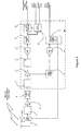
- FIG. 6 shows a receiver in accordance with the first embodiment of the present invention. The salient features of this new architecture will now be described in detail.
- a radio frequency TDMA signal is received by antenna 1 which is connected to the chain of filters 2/5/7 , amplifiers 3/6 and down-conversion stages 4 which comprise the analogue section of the receiver and which correspond to the like-numbered parts of Figure 2 and 3.
- the gain of amplifier chain 6 is set such that on receipt of a suitably modulated signal, at any arbitrary level within the dynamic range of the radio receiver, the output is driven into saturation (hard-limited) and stripped of its amplitude variations. Accordingly, at the output of amplifier 6 the signal approximates a variable duty cycle square-wave whose absolute phase is defined implicitly by the timings of its high-to-low and low-to-high transitions.
- Interpolation filter 7 performs time-to-voltage conversion from transitions applied at its input and in so doing regenerates the continuous phase/time characteristic of the down-converted radio frequency TDMA signal received at the input to amplifier chain 6 .
- this signal will be referred to as the 'Absolute Phase signal' and other signal names are allocated as appropriate.
- a signal characterising the received signal strength is also derived from circuits associated with the limiting amplifier chain 6 .
- this 'Amplitude signal' normally has a logarithmic relationship with applied input signal level a feature which, whilst not essential for the present purpose, can be exploited to reduce the dynamic range required of subsequent circuit blocks most notably the analogue-to-digital converter (ADC) 14 used for digitisation.
- ADC analogue-to-digital converter
- ADCs 8 and 14 digitise the Absolute Phase and Amplitude signals respectively to form corresponding sequences of digital Absolute Phase and Amplitude samples.
- the ADCs' sampling clocks are synchronised from a common time reference although they needn't necessarily operate at a common sampling frequency or phase.
- Samples from the Absolute Phase sequence are numerically processed by Differential Phase Detector 9 to form a 'Differential Phase sequence'.
- the Differential Phase sequence characterises the phase shift between adjacent samples in the Absolute Phase sequence or between samples separated by more than 1 digitising sample period.
- One algorithm for computing a complex Differential Phase sequence from the source Absolute Phase sequence is illustrated by the signal flow diagram in Figure 8. It will be recognised that there are several other methods for deriving the former from the latter and that all such methods may be used within the scope of the present invention.
- the Envelope Extractor 22 numerically processes the samples from the Amplitude sequence to derive a new sequence of what are hereafter referred to as Envelope Coefficients. This will be described in detail below, after an outline of the second embodiment has been given.
- FIG. 7 shows a receiver in accordance with the second embodiment of the present invention.
- the salient features of this new architecture will now be described in detail.
- the analogue section of the receiver is similar to that described previously in Figure 3.
- the limiting amplifier block c8 produces a constant-envelope, 'Phase' signal component at the output of interpolation filter c9 together with an 'Amplitude' signal component at the output of the signal strength detector c15 which has a response time commensurate with channel bandwidth thereby allowing symbol-rate variations in the received signal amplitude to be followed.
- this Amplitude signal has a logarithmic relationship with applied input signal level a feature which, whilst not essential for the present purpose, can be exploited to reduce the dynamic range, and thus complexity and power consumption, required of subsequent circuit blocks most notably the ADC c16 used for digitisation.
- ADCs c10 and c16 digitise the Phase and Amplitude signals respectively to form corresponding sequences of Phase and Amplitude samples.
- the ADCs' sampling clocks are synchronised from a common time reference although they needn't necessarily operate at a common sampling frequency or phase.
- derivation of the "Phase” signal may be achieved by providing one or more cascaded amplifiers, a quadratune down-mixing circuit and analogue filters such that the "Phase” signal is produced as a complex baseband signal having two components, preferably orthogonal, which are subsequently digitised separately.
- the combined purpose of the Envelope Extraction 22 , c13 and subsequent Envelope Modulation 21 or Envelope Insertion c11 processes, and the main aspect of the present invention, is to introduce the amplitude variations on the Phase sequence (either differential or absolute phase) which would have been present had the received radio frequency TDMA signal been digitised at the output of a Linear receiver with its amplitude information intact and with the receiver gain set to use all of the available ADC dynamic range.
- the Envelope Extractor 22, c13 numerically processes the samples from the Amplitude sequence to derive a new sequence of what are hereafter referred to as Envelope Coefficients. At least one such Envelope Coefficient is generated for each sample in the digitised Phase sequence and the scheduling of the ADCs and subsequent numerical processing is organised in such a way that the time correspondence between Phase and Amplitude signals at the input to the Limiting amplifier is restored prior to recombination.
- Analogue delay stage 23 , c18 is included to compensate for differential signal path delays which can not be removed by other means.
- the processing performed by the Envelope Extractor depends upon the relationship between the Amplitude signal and the instantaneous magnitude of the received radio frequency TDMA signal.
- the following description considers the common case of a logarithmic power detector and derives the mathematical relationships underlying the numerical processing carried out by the Envelope Extractor and Envelope Modulator or Insertion.
- a pk is the sample of the Amplitude sequence corresponding to the peak received signal amplitude r Pk occurring over a particular segment of the TDMA burst and a n ( norm ) is the normalised value of an arbitrary Amplitude sample a n . Note that according to (4) the maximum value of a n (norm) is zero, all other values being negative.
- the relevant signal segment is stored in sequential, first-in-first-out (FIFO) buffer d 4 implemented with either a circular buffer or shift register.
- FIFO first-in-first-out
- a second such buffer d6 is necessary for the storage of corresponding Phase samples received during the same signal segment.
- the duration of the signal segment used for peak detection governs the delay through the receiver (RF input to data output), the amount of storage needed for Magnitude and Phase samples and the accuracy of the Envelope Insertion step to be described.
- the presence of preamble and Sync Word fields on the TDMA burst provide two main options in this respect:
- the first option is to detect the peak across the entire burst. This implies storing a complete burst's worth of Magnitude and Phase samples in the FIFO buffers and a decoding delay of at least 1 burst.
- Figure 9 depicts the second option, which exploits the presence of the preamble and Sync Word to reduce the delay and storage requirements as follows: Peak detector d2 is enabled to operate during the Sync Word segment of the received signal only which, due to the random nature of the sequence, is sufficient to provide an accurate estimate of the peak value across the burst as a whole. The detector is reset prior to the Sync Word window in the received timeslot and its value held at the end of the Sync Word window. Thereafter received Magnitude samples are normalised with respect to the held peak whether or not they exceed the peak value. Values of a n received after the end of the Sync Word and which do exceed a pk are clipped to give 0 after normalisation.
- the action of the hard-limiting amplifier prior to digitisation removes amplitude variations from the Absolute Phase signal and accordingly the magnitude of both the current and delayed samples in the preceding expression can be considered constant.
- the sequence ⁇ n of Differential Phase vectors form one input to the Envelope modulator 21 .
- This sequence which due to the action of the differential phase detector, can not be considered a linear representation of the received radio frequency TDMA signal, but again contains sufficient amplitude and phase information to allow a subsequent non-coherent demodulator/equaliser to mitigate intersymbol interference induced by a multipath channel.
Landscapes
- Engineering & Computer Science (AREA)
- Computer Networks & Wireless Communication (AREA)
- Signal Processing (AREA)
- Digital Transmission Methods That Use Modulated Carrier Waves (AREA)
- Radio Transmission System (AREA)
- Time-Division Multiplex Systems (AREA)
Claims (19)
- Procédé de démodulation d'un signal à modulation de phase et/ou d'amplitude reçu comprenant les étapes consistant à :dériver dudit signal reçu une première séquence d'échantillons représentatifs de la phase du signal reçu ;dériver dudit signal reçu une seconde séquence d'échantillons représentatifs de l'enveloppe du signal reçu ;combiner les échantillons respectifs de ladite première séquence et de ladite seconde séquence pour produire une séquence composite d'échantillons représentatifs dudit signal reçu ; etdémoduler ladite séquence composite d'échantillons.
- Procédé selon la revendication 1, dans lequel ladite seconde séquence d'échantillons est dérivée d'un signal de temps continu ayant une relation logarithmique avec le niveau du signal reçu.
- Procédé selon la revendication 1 ou 2, dans lequel ladite étape de dérivation de ladite seconde séquence d'échantillons comprend les étapes consistant à :dériver dudit signal reçu un signal de temps continu représentatif de l'amplitude ou de la puissance instantanée du signal reçu ;numériser ledit signal de temps continu et stocker les échantillons numériques générés par lui ;déterminer une valeur de référence des échantillons stockés pendant une durée prédéterminée ; etnormaliser lesdits échantillons numériques stockés en utilisant ladite valeur de référence pour produire ladite seconde séquence d'échantillons.
- Procédé selon la revendication 3, dans lequel ladite valeur de référence est la valeur d'amplitude ou de puissance de pointe dans ladite durée prédéterminée.
- Procédé selon la revendication 1, 2, 3 ou 4, dans lequel ladite étape de dérivation de ladite première séquence d'échantillons comprend
l'amplification à limitation stricte dudit signal reçu et l'exécution de la détection de phase sur le signal amplifié pour générer un signal de temps continu représentatif de la phase absolue du signal reçu ; et
la numérisation dudit signal de temps continu pour produire ladite première séquence d'échantillons, de telle sorte que ladite première séquence d'échantillons soit une séquence d'échantillons représentant la phase absolue du signal reçu. - Procédé selon la revendication 1, 2, 3 ou 4, dans lequel ladite étape de dérivation de ladite première séquence d'échantillons comprend
l'amplification à limitation stricte dudit signal reçu et l'exécution de la détection de phase sur le signal amplifié pour générer un signal de temps continu représentatif de la phase absolue du signal reçu ; et
la numérisation dudit signal de temps continu pour produire une séquence d'échantillons de phase absolue ; et
l'exécution de la détection de phase différentielle sur ladite séquence d'échantillons de phase absolue pour produire ladite première séquence d'échantillons, de telle sorte que les échantillons dans ladite première séquence caractérise le déphasage entre paires d'échantillons avec un écart d'un nombre prédéterminé de périodes de numérisation d'échantillons. - Procédé selon la revendication 5 ou 6, comprenant en outre le stockage de ladite première séquence d'échantillons et la fourniture de chacun de ladite première séquence d'échantillons pour ladite étape de combinaison à des moments synchronisés avec ladite seconde séquence d'échantillons.
- Procédé selon l'une quelconque des revendications précédentes, ledit signal reçu étant un signal TDMA.
- Dispositif agencé pour recevoir un signal modulé en phase et/ou en amplitude comprenant :un moyen (6, 7, 8, c8, c9, c10) agencé pour dériver dudit signal reçu une première séquence d'échantillons représentatifs de la phase du signal reçu ;un moyen (6, 17, 14, c8, c15, c16) agencé pour dériver dudit signal reçu une seconde séquence d'échantillons représentatifs de l'enveloppe du signal reçu ; etun moyen (21, 22, c11, c13) agencé pour combiner les échantillons respectifs de ladite première séquence et de ladite seconde séquence d'échantillons et pour produire une représentation démodulée dudit signal reçu.
- Dispositif selon la revendication 9, dans lequel ledit moyen agencé pour dériver ladite seconde séquence d'échantillons est agencé pour dériver ladite seconde séquence d'un signal de temps continu ayant une relation logarithmique avec le niveau de signal reçu.
- Dispositif selon la revendication 9 ou 10 dans lequel ledit moyen agencé pour dériver ladite seconde séquence d'échantillons comprend
un moyen (17 ; c15) agencé pour dériver dudit signal reçu un signal de temps continu représentatif de l'amplitude ou de la puissance instantanée dudit signal reçu ;
un moyen de numérisation (14 ; c16) agencé pour numériser ledit signal de temps continu ;
un moyen de stockage agencé pour stocker les échantillons numériques dudit moyen de numérisation ;
un moyen de détermination (22 ; c13) agencé pour déterminer une valeur de référence des échantillons stockés sur une durée prédéterminée ; et un moyen de normalisation agencé pour normaliser lesdits échantillons stockés dans ledit moyen de stockage en utilisant ladite valeur de référence pour produire ladite seconde séquence d'échantillons. - Dispositif selon la revendication 11 dans lequel ledit moyen de détermination est agencé pour déterminer ladite valeur de référence de telle sorte qu'elle soit la valeur d'amplitude ou de puissance de pointe dans ladite durée prédéterminée.
- Dispositif selon la revendication 9, 10, 11 ou 12 dans lequel ledit moyen agencé pour dériver ladite première séquence d'échantillons comprend :un moyen d'amplification à limitation stricte et de détection de phase (c8) agencé pour générer un signal de temps continu représentatif de la phase absolue du signal reçu ; etun moyen de numérisation (c10) agencé pour numériser ledit signal de temps continu pour produire ladite première séquence d'échantillons, de telle sorte que ladite première séquence d'échantillons soit une séquence d'échantillons représentant la phase absolue du signal reçu.
- Dispositif selon la revendication 9, 10, 11 ou 12, dans lequel ledit moyen agencé pour dériver ladite première séquence d'échantillons comprend :un moyen d'amplification à limitation stricte et de détection de phase (6) agencé pour générer un signal de temps continu représentatif de la phase absolue du signal reçu ;un moyen de numérisation (8) agencé pour numériser ledit signal de temps continu pour produire une séquence d'échantillons de phase absolue ; etun moyen de détection de phase différentielle (9) agencé pour exécuter la détection de phase différentielle sur ladite séquence d'échantillons de phase absolue pour produire ladite première séquence d'échantillons, de telle sorte que les échantillons dans la première séquence caractérisent le déphasage entre les paires d'échantillons avec un écart d'un nombre prédéterminé de périodes de numérisation d'échantillons.
- Dispositif selon la revendication 13 ou 14, comprenant en outre un moyen de stockage agencé pour stocker ladite première séquence d'échantillons et pour produire chacun desdits échantillons de la première séquence à des moments synchronisés avec ladite seconde séquence d'échantillons.
- Dispositif selon la revendication 13, 14 ou 15, dans lequel ledit moyen d'amplification à limitation stricte et de détection de phase comprend un ou plusieurs amplificateurs en cascades et filtres analogiques agencés pour produire ledit signal de temps continu à une fréquence intermédiaire réelle.
- Dispositif selon la revendication 13, 14 ou 15, dans lequel ledit moyen d'amplification à limitation stricte et de détection de phase comprend un ou plusieurs amplificateurs en cascade, un circuit de réduction par mixage en quadrature et des filtres analogiques agencés pour produire ledit signal de temps continu sous forme de signal dans la bande de base complexe ayant deux composantes.
- Dispositif selon la revendication 17, dans lequel lesdites deux composantes sont orthogonales.
- Dispositif selon l'une quelconque des revendications 9 à 18 agencé pour recevoir et démoduler un signal TDMA.
Applications Claiming Priority (5)
| Application Number | Priority Date | Filing Date | Title |
|---|---|---|---|
| GBGB9702304.8A GB9702304D0 (en) | 1997-02-05 | 1997-02-05 | Non-coherent digital demodulator |
| GB9702304 | 1997-02-05 | ||
| GBGB9709713.3A GB9709713D0 (en) | 1997-05-13 | 1997-05-13 | Digital demodulator |
| GB9709713 | 1997-05-13 | ||
| PCT/GB1998/000355 WO1998035477A1 (fr) | 1997-02-05 | 1998-02-05 | Demodulation a branches phase et amplitude distinctes |
Publications (2)
| Publication Number | Publication Date |
|---|---|
| EP0958686A1 EP0958686A1 (fr) | 1999-11-24 |
| EP0958686B1 true EP0958686B1 (fr) | 2003-08-27 |
Family
ID=26310935
Family Applications (1)
| Application Number | Title | Priority Date | Filing Date |
|---|---|---|---|
| EP98903136A Expired - Lifetime EP0958686B1 (fr) | 1997-02-05 | 1998-02-05 | Demodulation a branches phase et amplitude distinctes |
Country Status (5)
| Country | Link |
|---|---|
| US (1) | US7349493B2 (fr) |
| EP (1) | EP0958686B1 (fr) |
| JP (1) | JP2001510661A (fr) |
| DE (1) | DE69817534T2 (fr) |
| WO (1) | WO1998035477A1 (fr) |
Families Citing this family (13)
| Publication number | Priority date | Publication date | Assignee | Title |
|---|---|---|---|---|
| JP3468287B2 (ja) | 1999-10-13 | 2003-11-17 | 日本電気株式会社 | Cdma受信agc回路およびcdma復調装置 |
| GB0130842D0 (en) * | 2001-12-21 | 2002-02-06 | Fizzle Holdings Ltd | Antenna measurement system |
| DE10208415B4 (de) | 2002-02-27 | 2006-03-16 | Advanced Micro Devices, Inc., Sunnyvale | Verstärkungsregelung in WLAN-Geräten |
| KR100459715B1 (ko) * | 2002-08-09 | 2004-12-03 | 삼성전자주식회사 | 고속의 디지털 RSSI(Received Signal Strength Indicator) 회로 |
| US8098778B2 (en) * | 2007-11-27 | 2012-01-17 | Infineon Technologies Ag | Controlled transmission of data in a data transmission system |
| KR101179126B1 (ko) * | 2010-03-31 | 2012-09-07 | 전자부품연구원 | 자기장 통신 방법 및 이에 의해 동작하는 노드 |
| US8149529B2 (en) * | 2010-07-28 | 2012-04-03 | Lsi Corporation | Dibit extraction for estimation of channel parameters |
| EP2755341B1 (fr) * | 2013-01-11 | 2016-01-06 | Telefonaktiebolaget L M Ericsson (publ) | Synchronisation pour reconfiguration radio |
| US9129650B2 (en) * | 2013-07-25 | 2015-09-08 | Avago Technologies General Ip (Singapore) Pte. Ltd. | Array-reader based magnetic recording systems with frequency division multiplexing |
| US9129651B2 (en) * | 2013-08-30 | 2015-09-08 | Avago Technologies General Ip (Singapore) Pte. Ltd. | Array-reader based magnetic recording systems with quadrature amplitude modulation |
| CN108572469B (zh) * | 2018-07-20 | 2023-09-26 | 中国人民解放军国防科技大学 | 多路不同频点激光同步相位调制光谱展宽装置及方法 |
| US10785015B1 (en) * | 2019-04-30 | 2020-09-22 | Keyssa Systems, Inc. | Multiple phase symbol synchronization for amplifier sampler accepting modulated signal |
| JP7680491B2 (ja) * | 2023-04-13 | 2025-05-20 | 日本無線株式会社 | 無線受信装置およびバースト検出方法 |
Family Cites Families (5)
| Publication number | Priority date | Publication date | Assignee | Title |
|---|---|---|---|---|
| US5001727A (en) * | 1989-02-15 | 1991-03-19 | Terra Marine Engineering, Inc. | Carrier and data recovery and demodulation system |
| US5608763A (en) * | 1993-12-30 | 1997-03-04 | Motorola, Inc. | Method and apparatus for decoding a radio frequency signal containing a sequence of phase values |
| JPH088987A (ja) * | 1994-06-23 | 1996-01-12 | Toshiba Corp | 位相検出装置 |
| JP3455934B2 (ja) * | 1995-04-11 | 2003-10-14 | 日本電信電話株式会社 | 変調器 |
| TW297965B (fr) * | 1995-06-26 | 1997-02-11 | Hitachi Ltd |
-
1998
- 1998-02-05 EP EP98903136A patent/EP0958686B1/fr not_active Expired - Lifetime
- 1998-02-05 WO PCT/GB1998/000355 patent/WO1998035477A1/fr not_active Ceased
- 1998-02-05 JP JP53399298A patent/JP2001510661A/ja active Pending
- 1998-02-05 DE DE69817534T patent/DE69817534T2/de not_active Expired - Lifetime
-
2003
- 2003-09-10 US US10/658,379 patent/US7349493B2/en not_active Expired - Lifetime
Also Published As
| Publication number | Publication date |
|---|---|
| EP0958686A1 (fr) | 1999-11-24 |
| JP2001510661A (ja) | 2001-07-31 |
| WO1998035477A1 (fr) | 1998-08-13 |
| US7349493B2 (en) | 2008-03-25 |
| DE69817534T2 (de) | 2004-05-27 |
| US20050073944A1 (en) | 2005-04-07 |
| DE69817534D1 (de) | 2003-10-02 |
Similar Documents
| Publication | Publication Date | Title |
|---|---|---|
| EP0842568B1 (fr) | Dispositif adaptatif de desetalement de spectre | |
| US8583067B2 (en) | Apparatus and method for improved wireless communication reliability and performance in process control systems | |
| CA1288878C (fr) | Extraction sans sequence de synchronisation initiale du signal d'horloge etde la porteuse faisant partie d'un signal amrt | |
| EP0474491B1 (fr) | Procédé et dispositif de traitement d'un signal de donnée reçu par voie radio | |
| US4291410A (en) | Multipath diversity spread spectrum receiver | |
| US5127025A (en) | Space diversity tdma receiver | |
| EP1072105B1 (fr) | Emetteur-recepteur a etalement de spectre d'un reseau local sans fil a attenuation multivoies | |
| US4873683A (en) | TDMA radio system employing BPSK synchronization for QPSK signals subject to random phase variation and multipath fading | |
| EP0958686B1 (fr) | Demodulation a branches phase et amplitude distinctes | |
| MXPA98000853A (en) | Des-extendedor adapta | |
| JP3168610B2 (ja) | 受信機 | |
| JP3723653B2 (ja) | デジタル移動電話装置 | |
| KR0172967B1 (ko) | 직렬 데이타 시스템에서 신호 패킷을 회복하는 장치 및 방법 | |
| KR100255726B1 (ko) | 자동 주파수 제어방법 및 장치 | |
| US8625564B2 (en) | Contact detection based radio channel selection apparatus and method | |
| JP2008530951A (ja) | 予め符号化された部分応答信号用の復調器および受信器 | |
| JP2977396B2 (ja) | 無線受信機 | |
| Metaxakis et al. | A low complexity baseband receiver for direct conversion DECT-based portable communication systems | |
| Wymeersch et al. | Blind symbol rate detection for low-complexity multi-rate receivers | |
| JP3718577B2 (ja) | 無線受信機及び無線受信方法 | |
| WO2001011844A1 (fr) | Demodulateur orthogonal et procede de demodulation orthogonale | |
| JP2591263B2 (ja) | 適応型受信機 | |
| Dimitriou et al. | Timing recovery scheme for CV-CCMA receiver | |
| JPH0697973A (ja) | 無線受信機 | |
| Tzimas et al. | A low complexity baseband receiver for direct conversion burst-type radio systems |
Legal Events
| Date | Code | Title | Description |
|---|---|---|---|
| PUAI | Public reference made under article 153(3) epc to a published international application that has entered the european phase |
Free format text: ORIGINAL CODE: 0009012 |
|
| 17P | Request for examination filed |
Effective date: 19990825 |
|
| AK | Designated contracting states |
Kind code of ref document: A1 Designated state(s): DE FI FR GB SE |
|
| GRAG | Despatch of communication of intention to grant |
Free format text: ORIGINAL CODE: EPIDOS AGRA |
|
| 17Q | First examination report despatched |
Effective date: 20020125 |
|
| GRAG | Despatch of communication of intention to grant |
Free format text: ORIGINAL CODE: EPIDOS AGRA |
|
| GRAH | Despatch of communication of intention to grant a patent |
Free format text: ORIGINAL CODE: EPIDOS IGRA |
|
| GRAS | Grant fee paid |
Free format text: ORIGINAL CODE: EPIDOSNIGR3 |
|
| GRAA | (expected) grant |
Free format text: ORIGINAL CODE: 0009210 |
|
| AK | Designated contracting states |
Designated state(s): DE FI FR GB SE |
|
| REG | Reference to a national code |
Ref country code: GB Ref legal event code: FG4D |
|
| REF | Corresponds to: |
Ref document number: 69817534 Country of ref document: DE Date of ref document: 20031002 Kind code of ref document: P |
|
| REG | Reference to a national code |
Ref country code: SE Ref legal event code: TRGR |
|
| ET | Fr: translation filed | ||
| PLBE | No opposition filed within time limit |
Free format text: ORIGINAL CODE: 0009261 |
|
| STAA | Information on the status of an ep patent application or granted ep patent |
Free format text: STATUS: NO OPPOSITION FILED WITHIN TIME LIMIT |
|
| 26N | No opposition filed |
Effective date: 20040528 |
|
| PGFP | Annual fee paid to national office [announced via postgrant information from national office to epo] |
Ref country code: FI Payment date: 20130227 Year of fee payment: 16 Ref country code: DE Payment date: 20130227 Year of fee payment: 16 Ref country code: FR Payment date: 20130311 Year of fee payment: 16 Ref country code: GB Payment date: 20130227 Year of fee payment: 16 Ref country code: SE Payment date: 20130227 Year of fee payment: 16 |
|
| REG | Reference to a national code |
Ref country code: DE Ref legal event code: R119 Ref document number: 69817534 Country of ref document: DE |
|
| REG | Reference to a national code |
Ref country code: SE Ref legal event code: EUG |
|
| GBPC | Gb: european patent ceased through non-payment of renewal fee |
Effective date: 20140205 |
|
| PG25 | Lapsed in a contracting state [announced via postgrant information from national office to epo] |
Ref country code: FI Free format text: LAPSE BECAUSE OF NON-PAYMENT OF DUE FEES Effective date: 20140205 |
|
| REG | Reference to a national code |
Ref country code: FR Ref legal event code: ST Effective date: 20141031 |
|
| PG25 | Lapsed in a contracting state [announced via postgrant information from national office to epo] |
Ref country code: SE Free format text: LAPSE BECAUSE OF NON-PAYMENT OF DUE FEES Effective date: 20140206 |
|
| REG | Reference to a national code |
Ref country code: DE Ref legal event code: R119 Ref document number: 69817534 Country of ref document: DE Effective date: 20140902 |
|
| PG25 | Lapsed in a contracting state [announced via postgrant information from national office to epo] |
Ref country code: GB Free format text: LAPSE BECAUSE OF NON-PAYMENT OF DUE FEES Effective date: 20140205 Ref country code: FR Free format text: LAPSE BECAUSE OF NON-PAYMENT OF DUE FEES Effective date: 20140228 Ref country code: DE Free format text: LAPSE BECAUSE OF NON-PAYMENT OF DUE FEES Effective date: 20140902 |