EP0959540A2 - Laser à semi-conducteur à puissance élevée - Google Patents
Laser à semi-conducteur à puissance élevée Download PDFInfo
- Publication number
- EP0959540A2 EP0959540A2 EP99109559A EP99109559A EP0959540A2 EP 0959540 A2 EP0959540 A2 EP 0959540A2 EP 99109559 A EP99109559 A EP 99109559A EP 99109559 A EP99109559 A EP 99109559A EP 0959540 A2 EP0959540 A2 EP 0959540A2
- Authority
- EP
- European Patent Office
- Prior art keywords
- layer
- active layer
- type
- type dopant
- semiconductor laser
- Prior art date
- Legal status (The legal status is an assumption and is not a legal conclusion. Google has not performed a legal analysis and makes no representation as to the accuracy of the status listed.)
- Granted
Links
Images
Classifications
-
- H—ELECTRICITY
- H10—SEMICONDUCTOR DEVICES; ELECTRIC SOLID-STATE DEVICES NOT OTHERWISE PROVIDED FOR
- H10H—INORGANIC LIGHT-EMITTING SEMICONDUCTOR DEVICES HAVING POTENTIAL BARRIERS
- H10H20/00—Individual inorganic light-emitting semiconductor devices having potential barriers, e.g. light-emitting diodes [LED]
- H10H20/80—Constructional details
- H10H20/81—Bodies
- H10H20/822—Materials of the light-emitting regions
- H10H20/824—Materials of the light-emitting regions comprising only Group III-V materials, e.g. GaP
- H10H20/8242—Materials of the light-emitting regions comprising only Group III-V materials, e.g. GaP characterised by the dopants
-
- H—ELECTRICITY
- H01—ELECTRIC ELEMENTS
- H01S—DEVICES USING THE PROCESS OF LIGHT AMPLIFICATION BY STIMULATED EMISSION OF RADIATION [LASER] TO AMPLIFY OR GENERATE LIGHT; DEVICES USING STIMULATED EMISSION OF ELECTROMAGNETIC RADIATION IN WAVE RANGES OTHER THAN OPTICAL
- H01S5/00—Semiconductor lasers
- H01S5/20—Structure or shape of the semiconductor body to guide the optical wave ; Confining structures perpendicular to the optical axis, e.g. index or gain guiding, stripe geometry, broad area lasers, gain tailoring, transverse or lateral reflectors, special cladding structures, MQW barrier reflection layers
- H01S5/22—Structure or shape of the semiconductor body to guide the optical wave ; Confining structures perpendicular to the optical axis, e.g. index or gain guiding, stripe geometry, broad area lasers, gain tailoring, transverse or lateral reflectors, special cladding structures, MQW barrier reflection layers having a ridge or stripe structure
- H01S5/227—Buried mesa structure ; Striped active layer
-
- H—ELECTRICITY
- H01—ELECTRIC ELEMENTS
- H01S—DEVICES USING THE PROCESS OF LIGHT AMPLIFICATION BY STIMULATED EMISSION OF RADIATION [LASER] TO AMPLIFY OR GENERATE LIGHT; DEVICES USING STIMULATED EMISSION OF ELECTROMAGNETIC RADIATION IN WAVE RANGES OTHER THAN OPTICAL
- H01S5/00—Semiconductor lasers
- H01S5/30—Structure or shape of the active region; Materials used for the active region
- H01S5/305—Structure or shape of the active region; Materials used for the active region characterised by the doping materials used in the laser structure
-
- H—ELECTRICITY
- H01—ELECTRIC ELEMENTS
- H01S—DEVICES USING THE PROCESS OF LIGHT AMPLIFICATION BY STIMULATED EMISSION OF RADIATION [LASER] TO AMPLIFY OR GENERATE LIGHT; DEVICES USING STIMULATED EMISSION OF ELECTROMAGNETIC RADIATION IN WAVE RANGES OTHER THAN OPTICAL
- H01S5/00—Semiconductor lasers
- H01S5/20—Structure or shape of the semiconductor body to guide the optical wave ; Confining structures perpendicular to the optical axis, e.g. index or gain guiding, stripe geometry, broad area lasers, gain tailoring, transverse or lateral reflectors, special cladding structures, MQW barrier reflection layers
- H01S5/22—Structure or shape of the semiconductor body to guide the optical wave ; Confining structures perpendicular to the optical axis, e.g. index or gain guiding, stripe geometry, broad area lasers, gain tailoring, transverse or lateral reflectors, special cladding structures, MQW barrier reflection layers having a ridge or stripe structure
- H01S5/227—Buried mesa structure ; Striped active layer
- H01S5/2275—Buried mesa structure ; Striped active layer mesa created by etching
-
- H—ELECTRICITY
- H01—ELECTRIC ELEMENTS
- H01S—DEVICES USING THE PROCESS OF LIGHT AMPLIFICATION BY STIMULATED EMISSION OF RADIATION [LASER] TO AMPLIFY OR GENERATE LIGHT; DEVICES USING STIMULATED EMISSION OF ELECTROMAGNETIC RADIATION IN WAVE RANGES OTHER THAN OPTICAL
- H01S5/00—Semiconductor lasers
- H01S5/30—Structure or shape of the active region; Materials used for the active region
- H01S5/305—Structure or shape of the active region; Materials used for the active region characterised by the doping materials used in the laser structure
- H01S5/3054—Structure or shape of the active region; Materials used for the active region characterised by the doping materials used in the laser structure p-doping
-
- H—ELECTRICITY
- H01—ELECTRIC ELEMENTS
- H01S—DEVICES USING THE PROCESS OF LIGHT AMPLIFICATION BY STIMULATED EMISSION OF RADIATION [LASER] TO AMPLIFY OR GENERATE LIGHT; DEVICES USING STIMULATED EMISSION OF ELECTROMAGNETIC RADIATION IN WAVE RANGES OTHER THAN OPTICAL
- H01S5/00—Semiconductor lasers
- H01S5/30—Structure or shape of the active region; Materials used for the active region
- H01S5/32—Structure or shape of the active region; Materials used for the active region comprising PN junctions, e.g. hetero- or double- heterostructures
- H01S5/3211—Structure or shape of the active region; Materials used for the active region comprising PN junctions, e.g. hetero- or double- heterostructures characterised by special cladding layers, e.g. details on band-discontinuities
Definitions
- the present invention relates to a semiconductor laser and, more particularly, to a semiconductor laser characterized by a carrier block portion for an active layer.
- a semiconductor laser is a light emitting device used in a broad range of fields such as optical communication, various optical measurements, and optical recording.
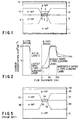
- FIG. 5 shows the structure of a 1.48- ⁇ m semiconductor laser for exciting an erbium-doped fiber amplifier used in the field of optical fiber communication.
- a mesa structure is formed on an n-type InP substrate 51.
- an InGaAsP separate confinement heterostructure (SCH) layer 52 an InGaAsP active layer 53, an InGaAsP SCH layer 54, and a p-type InP cladding layer 55 are stacked in this order.
- SCH separate confinement heterostructure
- the InGaAsP SCH layers 52 and 54 have a bandgap intermediate between the active layer 53 and the InP layers 51 and 55 and can have either a uniform structure or an internal refractive index distribution (to be referred to as a GRIN structure hereinafter).
- the InGaAsP active layer 53 often has a multiple quantum well structure (MQW) in which quantum well layers and barrier layers are stacked, rather than a bulk structure.
- MQW multiple quantum well structure
- active layer when a term "active layer" is used it doesn't matter whether the active layer has a bulk structure or an MQW structure.
- SCH layer has a uniform refractive index or a GRIN structure.
- a p-type InP buried layer 56 and an n-type InP buried layer 57 are buried in the two sides of the mesa to contribute to the constriction of a current path and the formation of a stripe optical waveguide.
- a p-type InGaAs contact layer 58 is formed on the p-type InP cladding layer 55 in many instances.
- a semiconductor layer is completed by forming metal electrodes on the two surfaces of the semiconductor crystal thus formed.
- Output of a semiconductor laser like this can be increased by many factors. Among other factors, it is important to allow radiative recombination at high probability of carriers (electrons and holes) injected into the active layer.
- a semiconductor laser like this often uses metal organic vapor phase epitaxy (MOVPE) having high mass productivity for crystal growth, Zn as a p-type dopant, and Si as an n-type dopant.
- MOVPE metal organic vapor phase epitaxy
- the doping amounts of these dopants control the carrier concentration in a semiconductor.
- Jpn. Pat. Appln. KOKAI Publication No. 7-193321 has disclosed a technique which decreases the doping concentration near an active layer and increases the doping concentration in a direction away from the active layer.
- Jpn. Pat. Appln. KOKAI Publication No. 9-45989 uses a method in which only a thin layer near an active layer is heavily doped and layers above this thin layer are lightly doped.
- This method uses C or Mg as a dopant instead of Zn which is readily diffusible.
- C or Mg must be used to suppress diffusion of a dopant to an active layer.
- the present invention has been made in consideration of the above situation, and has as its object to provide a semiconductor laser capable of preventing diffusion of a p-type dopant to an active layer while performing sufficient carrier blocking, even when Zn is used as a p-type dopant, and obtaining high emission efficiency and high output by minimizing light absorption in a p-type cladding layer.
- a semiconductor laser having a stacked structure including an n-type semiconductor substrate, an active layer, and a p-type cladding layer formed on the active layer, wherein the p-type cladding layer is formed such that regions doped with a p-type dopant are formed in an order of a first lightly doped region, a heavily doped region, and a second lightly doped region from a region closest to the active layer in a stacking direction, and a maximum value of concentration of the p-type dopant exists in the heavily doped region within a range of 50 to 250 nm in the stacking direction from the active layer.
- a semiconductor laser comprising:
- a method of fabricating a semiconductor laser comprising the steps of:
- an invention corresponding to the first aspect is a semiconductor laser having an active layer and a p-type cladding layer on an n-type semiconductor substrate, wherein the concentration distribution of a p-type dopant from the active layer to the p-type cladding layer has a maximum value at a distance of 50 to 250 nm from the end of the active layer.
- the present invention can perform carrier blocking for the active layer in the portion where the p-type dopant concentration has a maximum value.
- the distance from the position of this maximum value to the end of the active layer is at least 50 nm, so diffusion of the p-type dopant to the active layer can be prevented. Additionally, since the p-type dopant concentration decreases at least once after the position of the maximum value, light absorption in the p-type cladding layer can be minimized.
- the p-type dopant is zinc (Zn) in the invention corresponding to the first aspect.
- a lightly doped dopant region is formed between the active layer and the maximum value. Therefore, even when the p-type dopant is zinc which is readily diffusible, this dopant does not enter the active layer.
- the invention corresponding to this second aspect can achieve the same effects as in the invention corresponding to the first aspect and can also prevent degradation of the laser characteristics caused by an increase in non-radiative recombination resulting from mixing of zinc. It is also possible to use, as a dopant, a material which is inexpensive and pure, has been actually used in many applications, and hence is highly reliable.
- the material system of the semiconductor is InGaAsP/InP in the invention corresponding to the first or second aspect.
- the present invention can achieve the same effects as in the invention corresponding to the first or second aspect and can also provide a semiconductor laser required to have high output, e.g., a semiconductor laser usable to excite a fiber amplifier in the field of optical communication.
- the maximum value of the p-type dopant concentration is 1 ⁇ 10 18 /cm 3 or more in the inventions corresponding to the first to third aspects.
- the present invention can achieve the same effects as in the inventions corresponding to the first to third aspects and can also perform sufficient carrier blocking.
- the minimum value of the p-type dopant concentration from the end of the active layer to the heavily doped region maximum value is 3 ⁇ 10 17 /cm 3 or less in the inventions corresponding to the first to fourth aspects.
- the present invention can achieve the same effects as in the inventions corresponding to the first to fourth aspects and can also more effectively prevent mixing of the p-type dopant into the active layer.
- An invention corresponding to the sixth aspect has a separate confinement heterostructure layer between the active layer and the p-type cladding layer in the inventions corresponding to the first to fifth aspects.
- the present invention can achieve the same effects as in the inventions corresponding to the first to fifth aspects even when the separate confinement heterostructure layer is formed.
- the maximum value of the dopant concentration can exist in this separate confinement heterostructure layer.
- the active layer has a multiple quantum well structure in the inventions corresponding to the first to sixth aspects.
- the present invention can achieve the same effects as in the inventions corresponding to the first to sixth aspects and can also further improve the characteristics.
- An invention corresponding to the eighth aspect is a semiconductor laser having an active layer and a p-type cladding layer using zinc as a p-type dopant on an n-type semiconductor substrate, wherein a concentration distribution of the p-type dopant from the end of the active layer to the p-type cladding layer has at least one maximum value with the undoped region or lightly doped region sandwiched between the end of the active layer and the heavily doped region.
- the present invention can achieve the same effects as in the invention corresponding to the second aspect.
- FIG. 1 is a sectional view showing the arrangement of a semiconductor laser according to the embodiment of the present invention.
- This semiconductor laser is constructed in the same manner as the semiconductor laser explained in "BACKGROUND OF THE INVENTION” except for the concentration distribution in p-type cladding layers.
- an InGaAsP separate confinement heterostructure (SHC) layer 2 an InGaAsP active layer 3
- InGaAsP SCH layer 4 an InGaAsP SCH layer 4, and p-type InP cladding layers 5, 6, and 7 are stacked in this order.
- SHC InGaAsP separate confinement heterostructure
- the p-type cladding layers are three layers, i.e., the lightly doped p-type cladding layer 5, the heavily doped p-type cladding layer 6, and the moderately doped p-type cladding layer 7 formed in the order named from a layer closest to the active layer 3.
- a p-type contact layer 8 is stacked on the moderately doped p-type cladding layer 7.
- a p-type InP buried layer 9 and an n-type InP buried layer 10 are buried in the two sides of the mesa to contribute to the constriction of a current path and the formation of a stripe optical waveguide.
- an n-type electrode 11 and a p-type electrode 12 are formed on the n-type InP substrate 1 and the p-type contact layer 8, respectively, to complete the semiconductor laser.
- the dopant used in the p-type cladding layers 5, 6, and 7 is zinc (Zn), and the carrier concentrations in these layers 5, 6, and 7 and the carrier concentration distribution in the direction of thickness of these layers are important.
- FIG. 2 shows an example of the carrier concentration distribution in the p-type cladding layers in the semiconductor laser of this embodiment.
- a first portion 50 nm thick from the end portion of the active layer is lightly doped (the lightly doped p-type cladding layer 5).
- a portion 100 nm thick from the end of this lightly doped p-type cladding layer 5 (i.e., a portion within the range of 50 to 150 nm from the end portion of the active layer 3) is heavily doped (the heavily doped p-type cladding layer 6).
- the solid line indicates the carrier concentration distribution when the cladding layers are stacked.
- the alternate long and short dashed line indicates the carrier concentration in the finally obtained semiconductor laser.
- the first 50-nm thick portion from the end portion of the active layer 3 is lightly doped as described above, and this distance of 50 nm includes the thickness of the SCH layer 4.
- the subsequent heavily doped portion need not exist in the cladding layer, i.e., the heavily doped portion can exist in the SCH layer 4.
- the lightly doped p-type cladding layer 5, the heavily doped p-type cladding layer 6, and the moderately doped p-type cladding layer 7 are formed in the order named" in this specification means that layers lightly, heavily, and moderately doped with zinc (Zn) are formed in this order from the upper end of the active layer, regardless of whether each doped layer actually exists in the SCH layer 4 or the cladding layer (this relationship holds in the remainder of this specification).
- the heavily doped p-type cladding layer 6 functions as a carrier block for blocking electrons overflowing from the active layer 3.
- this heavily doped p-type cladding layer 6 is formed near the active layer 3, effective carrier blocking is performed, and a high-efficiency, high-output semiconductor laser is realized.
- the heavily doped p-type cladding layer 6 is formed near the active layer 3 as described above and, more importantly, the lightly doped p-type cladding layer 5 is formed between this heavily doped p-type cladding layer 6 and the active layer 3.
- the lightly doped p-type cladding layer 5 is desirably undoped or doped at a low concentration of about 3 ⁇ 10 17 /cm 3 or less.
- the formation of the moderately doped p-type cladding layer 7 having a medium carrier concentration in the portion following the heavily doped p-type cladding layer 6 also contributes to the realization of high emission efficiency and high output.
- a portion heavily doped with Zn is necessary to block carriers.
- the region moderately doped with Zn (the moderately doped p-type cladding layer 7) is formed after the heavily doped p-type cladding layer 6 as a carrier blocking layer.
- the hole concentration in the whole cladding layers is prevented from becoming too high, thereby suppressing light absorption by holes.
- the moderately doped p-type cladding layer 7 occupying the most part of the cladding layers preferably has a carrier concentration of about 5 ⁇ 10 17 /cm 3 as a whole.
- the carrier concentration distribution has a concentration peak (maximum value) as indicated by the alternate long and short dashed line in FIG. 2.
- the concentration decreases at least once from the position of this maximum value in a direction away from the active layer 3.
- the concentrations in the layers 5, 6, and 7 are so adjusted that the position of this p-type dopant concentration peak (maximum value) is at a distance of 50 to 250 nm (preferably 50 to 150 nm) from the end of the active layer 3.
- this maximum value point is at a distance of about 50 to 250 nm (preferably 50 to 150 nm) from the active layer 3, diffusion of Zn does not reach the active layer 3.
- the semiconductor laser of this embodiment constructed as above high emission efficiency can be obtained because electrons are well confined in the active layer and light loss caused by holes is small. Accordingly, the laser beam of this semiconductor laser has high output.
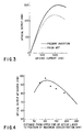
- FIG. 3 is a graph showing the output characteristic of the semiconductor laser of this embodiment.
- the semiconductor laser of this embodiment realizes output higher by 20% or more than a semiconductor laser of prior art.
- the aforementioned maximum value need not probably be the maximum value of the carrier concentration in the cladding layers.
- FIG. 4 is a graph showing the relationship between the distance of the maximum value of the carrier concentration in the p-type cladding layers from the upper end of the active layer.
- FIG. 4 shows the result of measurement of optical output for an injected current of 500 mA.
- the lightly doped p-type cladding layer 5 is an undoped layer, and neither a low- nor high-reflecting coating are formed.
- the semiconductor laser shown in FIG. 3 has low-and high-reflecting coatings, and output light from the low-reflecting coating is measured. Therefore, the apparent optical output is larger than in FIG. 4.
- an optimum distance from the upper end of the active layer to the position of the maximum value is about 100 nm.
- this distance is about 50 to 250 nm, a semiconductor laser having high light emission efficiency and high output can be obtained. More preferably, a considerably large output increasing effect can be obtained when the distance to the maximum value is about 50 to 150 nm.
- the lightly doped p-type cladding layer 5 is an undoped layer.
- the optical output does not become lower than that shown in FIG. 4 even if the position of the maximum concentration is farther from the upper end of the active layer.
- the heavily doped p-type cladding layer 6 is formed near the active layer 3 with the lightly doped p-type cladding layer 5 sandwiched between them. Therefore, even when Zn is used as a p-type dopant, this p-type dopant does not diffuse to the active layer 3. Additionally, electrons are well confined in the active layer 3 by blocking by the heavily doped layer 6. Consequently, high emission efficiency and high output can be realized.
- the moderately doped p-type cladding layer 7 is formed subsequently to the heavily doped p-type cladding layer 6 so that the final carrier concentration distribution takes a maximum value in the heavily doped p-type cladding layer 6. Additionally, the position of this maximum value is set within a predetermined range from the upper end of the active layer. Consequently, in addition to the above effects, absorption of light in the p-type cladding layers by holes can be minimized. This further increases the laser output.
- This practical example relates to steps of fabricating a 1.48- ⁇ m semiconductor laser for exciting an erbium-doped fiber amplifier used in the field of optical fiber communication.
- the structure of this semiconductor laser is the same as shown in FIG. 1.
- InGaAsP layers having compositions by which the bandgap wavelengths are 1.15, 1.08, and 0.99 ⁇ m and each having a thickness of 30 nm are stacked on an n-type InP substrate 1 having a carrier concentration of 1 ⁇ 10 18 /cm 3 by using MOVPE, thereby forming an SCH layer 2.
- a multiple quantum well structure active layer 3 having four well layers are grown on the SCH layer 2 by forming InGaAsP layers, in which -0.5% of tensile strain is introduced to a composition by which the bandgap wavelength is 1.25 ⁇ m with no strain, as barrier layers, and InGaAsP layers, in which +1% of compression strain is introduced to a composition by which the bandgap wavelength is 1.55 ⁇ m, as well layers.
- InGaAsP layers having compositions by which the bandgap wavelengths are 0.99, 1.08, and 1.15 ⁇ m and each having a thickness of 30 nm are stacked on the active layer 3, thereby forming an SCH layer 4.
- an undoped 50-nm thick InP layer, a p-type 100-nm thick InP layer having a carrier concentration of 1 ⁇ 10 18 /cm 3 , and a p-type 300-nm thick InP layer having a carrier concentration of 5 ⁇ 10 17 /cm 3 are stacked in this order as a lightly doped p-type cladding layer 5, a heavily doped p-type cladding layer 6, and a moderately doped p-type cladding layer 7, respectively, thereby forming the p-type cladding layers 5, 6, and 7.
- the dopant is zinc (Zn), and the carrier concentration of the lightly doped p-type cladding layer 5 can be about 3 ⁇ 10 17 /cm 3 .
- SiO 2 film about a few tens of nm thick is deposited on the p-type cladding layer 7 by plasma CVD or the like. This SiO 2 film is formed into a stripe about 2 ⁇ m wide by photolithography to form an etching mask.
- the resultant structure is dipped into an etching solution consisting of sulfuric acid, oxalic acid, and hydrochloric acid using this stripe SiO 2 film as an etching mask, thereby forming a mesa shape.
- the SiO 2 film is used as a growth inhibiting mask to sequentially stack and bury a p-type InP buried layer 9 and an n-type InP buried layer 10 in the mesa by MOVPE.
- a 2- ⁇ m thick p-type InP cladding layer 7 having a carrier concentration of 5 ⁇ 10 17 /cm 3 is grown on the entire surface from which the SiO 2 film is removed.
- a 0.5- ⁇ m thick p-type InGaAs contact layer 8 having a carrier concentration of 5 ⁇ 10 18 /cm 3 is grown.
- the n-type InP substrate 1 is polished to have a thickness of about 100 ⁇ m, a p-type electrode 12 containing Au and Zn is formed on the growth surface by vapor deposition, and an n-type electrode 11 containing Au and Ge is formed on the substrate surface by vapor deposition.
- n- and p-type electrodes 11 and 12 are plated with Au.
- the end faces on the two sides are cleaved, and a dielectric film as a low-reflecting coating or high-reflecting coating is formed on the cleaved end faces by vapor deposition or the like.
- the injected current-optical output characteristic of the present invention shown in FIG. 3 of the above embodiment is the characteristic measured for the semiconductor laser fabricated as above.
- the characteristic of the semiconductor laser according to the prior art shown in FIG. 3 is measured for a device fabricated by setting the carrier concentrations of all p-type cladding layers to a fixed value of 5 ⁇ 10 17 /cm 3 for comparison.
- FIG. 3 shows that the optical output of the semiconductor laser according to the embodiment of the present invention is higher by 20% or more than that of the semiconductor laser of the prior art when the injected current is 500A.
- the present invention has three GRIN SCH layers and a strained MQW structure active layer having four well layers.
- the present invention is not limited to these structures and is applicable to semiconductor lasers having various structures.
- a heavily doped region is formed with a lightly doped region sandwiched between an active layer and the heavily doped region. Therefore, it is possible to provide a semiconductor laser capable of preventing diffusion of a p-type dopant to an active layer while performing sufficient carrier blocking, even when Zn is used as a p-type dopant, and obtaining high emission efficiency and high output by minimizing light absorption in a p-type cladding layer.
Landscapes
- Physics & Mathematics (AREA)
- Condensed Matter Physics & Semiconductors (AREA)
- General Physics & Mathematics (AREA)
- Electromagnetism (AREA)
- Optics & Photonics (AREA)
- Geometry (AREA)
- Semiconductor Lasers (AREA)
Applications Claiming Priority (2)
| Application Number | Priority Date | Filing Date | Title |
|---|---|---|---|
| JP13180098A JP3481458B2 (ja) | 1998-05-14 | 1998-05-14 | 半導体レーザ |
| JP13180098 | 1998-05-14 |
Publications (3)
| Publication Number | Publication Date |
|---|---|
| EP0959540A2 true EP0959540A2 (fr) | 1999-11-24 |
| EP0959540A3 EP0959540A3 (fr) | 2000-02-02 |
| EP0959540B1 EP0959540B1 (fr) | 2002-08-07 |
Family
ID=15066414
Family Applications (1)
| Application Number | Title | Priority Date | Filing Date |
|---|---|---|---|
| EP99109559A Expired - Lifetime EP0959540B1 (fr) | 1998-05-14 | 1999-05-12 | Laser à semi-conducteur à puissance élevée |
Country Status (4)
| Country | Link |
|---|---|
| US (1) | US6351479B1 (fr) |
| EP (1) | EP0959540B1 (fr) |
| JP (1) | JP3481458B2 (fr) |
| DE (1) | DE69902421T2 (fr) |
Cited By (9)
| Publication number | Priority date | Publication date | Assignee | Title |
|---|---|---|---|---|
| EP0978912A3 (fr) * | 1998-08-07 | 2001-12-12 | Agere Systems Optoelectronics Guardian Corporation | Laser à puits quantiques multiples avec barrières à dopage sélective |
| WO2002019479A3 (fr) * | 2000-08-30 | 2003-02-13 | Federalnoe G Unitarnoe Predpr | Laser a injection |
| WO2002019480A3 (fr) * | 2000-08-30 | 2003-02-13 | Federalnoe G Unitarnoe Predpr | Procede de fabrication d'un laser a injection |
| WO2002019483A3 (fr) * | 2000-08-30 | 2003-02-13 | Federalnoe G Unitarnoe Predpr | Amelioration d'une bande de frequence utile de modulation laser |
| EP1168540A3 (fr) * | 2000-06-20 | 2003-04-02 | The Furukawa Electric Co., Ltd. | Dispositif laser à semiconducteur |
| EP1380077A4 (fr) * | 2001-03-19 | 2005-12-07 | Trumpf Photonics Inc | Procedes et appareils ameliorant l'efficacite de dispositifs sources de rayonnement optoelectronique |
| US7084444B2 (en) | 2001-03-19 | 2006-08-01 | Trumpf Photonics, Inc. | Method and apparatus for improving efficiency in opto-electronic radiation source devices |
| EP1717918A4 (fr) * | 2004-02-16 | 2007-05-16 | Anritsu Corp | Laser semi-conducteur longueur donde variable et capteur de gaz utilisant ledit laser |
| EP2053668A3 (fr) * | 2007-06-21 | 2010-04-07 | Sumitomo Electric Industries, Ltd. | Dispositif électroluminescent à semi-conducteur de nitrure de groupe III |
Families Citing this family (22)
| Publication number | Priority date | Publication date | Assignee | Title |
|---|---|---|---|---|
| FR2820891B1 (fr) * | 2001-02-13 | 2004-08-27 | Cit Alcatel | Laser semi conducteur a ruban enterre et procede de fabrication |
| JP2002299762A (ja) * | 2001-03-30 | 2002-10-11 | Nichia Chem Ind Ltd | 窒化物半導体素子 |
| KR100602973B1 (ko) * | 2003-10-30 | 2006-07-20 | 한국과학기술연구원 | 스트레인 보상 다층양자우물을 이용하는 단일모드형 레이저 다이오드 및 그 제조 방법 |
| JPWO2005074047A1 (ja) * | 2004-01-28 | 2008-01-10 | アンリツ株式会社 | 光半導体素子およびその製造方法 |
| JP2006128151A (ja) * | 2004-10-26 | 2006-05-18 | Mitsubishi Electric Corp | 半導体レーザ装置およびその製造方法 |
| JP2006253212A (ja) * | 2005-03-08 | 2006-09-21 | Sumitomo Electric Ind Ltd | 半導体レーザ |
| KR20070084973A (ko) * | 2006-02-22 | 2007-08-27 | 삼성전기주식회사 | 고출력 반도체 레이저소자 |
| JP4834690B2 (ja) * | 2008-04-24 | 2011-12-14 | アンリツ株式会社 | ガス検知装置用波長可変型半導体レーザ及びガス検知装置 |
| JP2010169625A (ja) * | 2009-01-26 | 2010-08-05 | Anritsu Corp | ガス検知装置 |
| JP2010192528A (ja) * | 2009-02-16 | 2010-09-02 | Anritsu Corp | 半導体光素子とそれを用いた波長掃引光源 |
| JP6291849B2 (ja) | 2014-01-10 | 2018-03-14 | 三菱電機株式会社 | 半導体装置の製造方法、半導体装置 |
| JP6519921B2 (ja) * | 2014-07-07 | 2019-05-29 | 住友電工デバイス・イノベーション株式会社 | 光半導体素子及び光半導体素子の製造方法 |
| US11056434B2 (en) * | 2017-01-26 | 2021-07-06 | Epistar Corporation | Semiconductor device having specified p-type dopant concentration profile |
| US10971652B2 (en) | 2017-01-26 | 2021-04-06 | Epistar Corporation | Semiconductor device comprising electron blocking layers |
| US10084282B1 (en) | 2017-08-14 | 2018-09-25 | The United States Of America As Represented By The Secretary Of The Air Force | Fundamental mode operation in broad area quantum cascade lasers |
| JP6414306B2 (ja) * | 2017-09-27 | 2018-10-31 | 三菱電機株式会社 | 半導体装置の製造方法、半導体装置 |
| US11031753B1 (en) | 2017-11-13 | 2021-06-08 | The Government Of The United States Of America As Represented By The Secretary Of The Air Force | Extracting the fundamental mode in broad area quantum cascade lasers |
| US10833480B2 (en) * | 2018-07-03 | 2020-11-10 | Skorpios Technologies, Inc. | Diffusion blocking layer for a compound semiconductor structure |
| CN112398003B (zh) * | 2019-08-19 | 2023-01-06 | 朗美通日本株式会社 | 调制掺杂半导体激光器及其制造方法 |
| US12489275B2 (en) * | 2020-01-28 | 2025-12-02 | Mitsubishi Electric Corporation | Method for manufacturing optical semiconductor device |
| JP7421989B2 (ja) * | 2020-04-02 | 2024-01-25 | 浜松ホトニクス株式会社 | 量子カスケードレーザ素子及び量子カスケードレーザ装置 |
| JP7330128B2 (ja) * | 2020-04-02 | 2023-08-21 | 浜松ホトニクス株式会社 | 量子カスケードレーザ素子及び量子カスケードレーザ装置 |
Family Cites Families (10)
| Publication number | Priority date | Publication date | Assignee | Title |
|---|---|---|---|---|
| EP0259026B1 (fr) | 1986-08-08 | 1994-04-27 | Kabushiki Kaisha Toshiba | Laser à semi-conducteur à double-hétérostructure avec un guide d'ondes à ruban mesa |
| DE69023956T2 (de) | 1989-06-16 | 1996-04-25 | Toshiba Kawasaki Kk | Verfahren zur Herstellung eines III-V-Verbindungshalbleiterbauelementes. |
| EP0571021B1 (fr) | 1992-05-18 | 1997-08-06 | Koninklijke Philips Electronics N.V. | Dispositif semiconducteur optoélectronique |
| JPH06222406A (ja) | 1993-01-26 | 1994-08-12 | Nippon Telegr & Teleph Corp <Ntt> | 半導体光デバイス |
| JP2699848B2 (ja) | 1993-12-27 | 1998-01-19 | 日本電気株式会社 | 半導体レーザの製造方法 |
| JP2778454B2 (ja) * | 1994-03-07 | 1998-07-23 | 日本電気株式会社 | 半導体レーザ |
| JPH07249575A (ja) * | 1994-03-09 | 1995-09-26 | Nippon Telegr & Teleph Corp <Ntt> | 半導体光素子の製造方法 |
| WO1996020522A1 (fr) | 1994-12-28 | 1996-07-04 | Mitsui Petrochemical Industries, Ltd. | Element de laser a semi-conducteur |
| JP3645320B2 (ja) | 1995-07-31 | 2005-05-11 | 三井化学株式会社 | 半導体レーザ素子 |
| JP3652072B2 (ja) * | 1997-07-30 | 2005-05-25 | シャープ株式会社 | 半導体レーザ素子 |
-
1998
- 1998-05-14 JP JP13180098A patent/JP3481458B2/ja not_active Expired - Lifetime
-
1999
- 1999-05-10 US US09/307,438 patent/US6351479B1/en not_active Expired - Lifetime
- 1999-05-12 DE DE69902421T patent/DE69902421T2/de not_active Expired - Lifetime
- 1999-05-12 EP EP99109559A patent/EP0959540B1/fr not_active Expired - Lifetime
Cited By (10)
| Publication number | Priority date | Publication date | Assignee | Title |
|---|---|---|---|---|
| EP0978912A3 (fr) * | 1998-08-07 | 2001-12-12 | Agere Systems Optoelectronics Guardian Corporation | Laser à puits quantiques multiples avec barrières à dopage sélective |
| EP1168540A3 (fr) * | 2000-06-20 | 2003-04-02 | The Furukawa Electric Co., Ltd. | Dispositif laser à semiconducteur |
| WO2002019479A3 (fr) * | 2000-08-30 | 2003-02-13 | Federalnoe G Unitarnoe Predpr | Laser a injection |
| WO2002019480A3 (fr) * | 2000-08-30 | 2003-02-13 | Federalnoe G Unitarnoe Predpr | Procede de fabrication d'un laser a injection |
| WO2002019483A3 (fr) * | 2000-08-30 | 2003-02-13 | Federalnoe G Unitarnoe Predpr | Amelioration d'une bande de frequence utile de modulation laser |
| EP1380077A4 (fr) * | 2001-03-19 | 2005-12-07 | Trumpf Photonics Inc | Procedes et appareils ameliorant l'efficacite de dispositifs sources de rayonnement optoelectronique |
| US7084444B2 (en) | 2001-03-19 | 2006-08-01 | Trumpf Photonics, Inc. | Method and apparatus for improving efficiency in opto-electronic radiation source devices |
| EP1717918A4 (fr) * | 2004-02-16 | 2007-05-16 | Anritsu Corp | Laser semi-conducteur longueur donde variable et capteur de gaz utilisant ledit laser |
| EP2053668A3 (fr) * | 2007-06-21 | 2010-04-07 | Sumitomo Electric Industries, Ltd. | Dispositif électroluminescent à semi-conducteur de nitrure de groupe III |
| US8829545B2 (en) | 2007-06-21 | 2014-09-09 | Sumitomo Electric Industries, Ltd. | Group III nitride semiconductor light-emitting device |
Also Published As
| Publication number | Publication date |
|---|---|
| EP0959540B1 (fr) | 2002-08-07 |
| EP0959540A3 (fr) | 2000-02-02 |
| DE69902421D1 (de) | 2002-09-12 |
| DE69902421T2 (de) | 2003-04-24 |
| JPH11330605A (ja) | 1999-11-30 |
| JP3481458B2 (ja) | 2003-12-22 |
| US6351479B1 (en) | 2002-02-26 |
Similar Documents
| Publication | Publication Date | Title |
|---|---|---|
| EP0959540B1 (fr) | Laser à semi-conducteur à puissance élevée | |
| US4928285A (en) | Impurity-doped semiconductor laser device for single wavelength oscillation | |
| US20090203161A1 (en) | Semiconductor laser diode with a ridge structure buried by a current blocking layer made of un-doped semiconductor grown at a low temperature and method for producing the same | |
| EP0805533B1 (fr) | Element de laser a semi-conducteur | |
| JPH0656906B2 (ja) | 半導体レ−ザ装置 | |
| JPH10200190A (ja) | 半導体レーザ及びその製造方法 | |
| CN118299928A (zh) | 一种半导体激光器及其制备方法 | |
| KR100232993B1 (ko) | 반도체 레이저장치 및 그 제조방법 | |
| US7430228B2 (en) | Semiconductor laser device and method of producing the same | |
| JP3135109B2 (ja) | 半導体発光素子 | |
| US5446753A (en) | Current block type semiconductor laser | |
| US7405421B2 (en) | Optical integrated device | |
| CN111129945B (zh) | 整片制作省隔离器边发射激光器芯片的方法 | |
| US7957442B2 (en) | Semiconductor optical device | |
| EP1981138A1 (fr) | Dispositif optique à semi-conducteur et son procédé de fabrication | |
| JP3658048B2 (ja) | 半導体レーザ素子 | |
| JP3645320B2 (ja) | 半導体レーザ素子 | |
| JP3645343B2 (ja) | 半導体レーザ素子 | |
| JP2000208870A (ja) | 半導体レ―ザおよびその製造方法 | |
| US20040095979A1 (en) | Semiconductor device and method for producing the same | |
| US7298769B2 (en) | Semiconductor laser | |
| JPH11233874A (ja) | 半導体レーザ装置およびその製造方法 | |
| JPH09232666A (ja) | 半導体レーザ及び並列伝送用光送信モジュール | |
| US20030063644A1 (en) | Semiconductor laser element having great bandgap difference between active layer and optical waveguide layers, and including arrow structure formed without P-As interdiffusion | |
| JPH0823139A (ja) | 半導体レーザ |
Legal Events
| Date | Code | Title | Description |
|---|---|---|---|
| PUAI | Public reference made under article 153(3) epc to a published international application that has entered the european phase |
Free format text: ORIGINAL CODE: 0009012 |
|
| 17P | Request for examination filed |
Effective date: 19990512 |
|
| AK | Designated contracting states |
Kind code of ref document: A2 Designated state(s): DE FR GB IT |
|
| AX | Request for extension of the european patent |
Free format text: AL;LT;LV;MK;RO;SI |
|
| PUAL | Search report despatched |
Free format text: ORIGINAL CODE: 0009013 |
|
| AK | Designated contracting states |
Kind code of ref document: A3 Designated state(s): AT BE CH CY DE DK ES FI FR GB GR IE IT LI LU MC NL PT SE |
|
| AX | Request for extension of the european patent |
Free format text: AL;LT;LV;MK;RO;SI |
|
| 17Q | First examination report despatched |
Effective date: 20000529 |
|
| AKX | Designation fees paid |
Free format text: DE FR GB IT |
|
| RIC1 | Information provided on ipc code assigned before grant |
Free format text: 7H 01S 5/32 A, 7H 01L 33/00 B |
|
| RIC1 | Information provided on ipc code assigned before grant |
Free format text: 7H 01S 5/32 A, 7H 01L 33/00 B |
|
| GRAG | Despatch of communication of intention to grant |
Free format text: ORIGINAL CODE: EPIDOS AGRA |
|
| GRAG | Despatch of communication of intention to grant |
Free format text: ORIGINAL CODE: EPIDOS AGRA |
|
| GRAH | Despatch of communication of intention to grant a patent |
Free format text: ORIGINAL CODE: EPIDOS IGRA |
|
| GRAH | Despatch of communication of intention to grant a patent |
Free format text: ORIGINAL CODE: EPIDOS IGRA |
|
| GRAA | (expected) grant |
Free format text: ORIGINAL CODE: 0009210 |
|
| AK | Designated contracting states |
Kind code of ref document: B1 Designated state(s): DE FR GB IT |
|
| REG | Reference to a national code |
Ref country code: GB Ref legal event code: FG4D |
|
| REF | Corresponds to: |
Ref document number: 69902421 Country of ref document: DE Date of ref document: 20020912 |
|
| ET | Fr: translation filed | ||
| PLBE | No opposition filed within time limit |
Free format text: ORIGINAL CODE: 0009261 |
|
| STAA | Information on the status of an ep patent application or granted ep patent |
Free format text: STATUS: NO OPPOSITION FILED WITHIN TIME LIMIT |
|
| 26N | No opposition filed |
Effective date: 20030508 |
|
| PGFP | Annual fee paid to national office [announced via postgrant information from national office to epo] |
Ref country code: GB Payment date: 20130508 Year of fee payment: 15 Ref country code: DE Payment date: 20130515 Year of fee payment: 15 |
|
| PGFP | Annual fee paid to national office [announced via postgrant information from national office to epo] |
Ref country code: IT Payment date: 20130522 Year of fee payment: 15 Ref country code: FR Payment date: 20130531 Year of fee payment: 15 |
|
| REG | Reference to a national code |
Ref country code: DE Ref legal event code: R119 Ref document number: 69902421 Country of ref document: DE |
|
| GBPC | Gb: european patent ceased through non-payment of renewal fee |
Effective date: 20140512 |
|
| REG | Reference to a national code |
Ref country code: DE Ref legal event code: R119 Ref document number: 69902421 Country of ref document: DE Effective date: 20141202 |
|
| REG | Reference to a national code |
Ref country code: FR Ref legal event code: ST Effective date: 20150130 |
|
| PG25 | Lapsed in a contracting state [announced via postgrant information from national office to epo] |
Ref country code: DE Free format text: LAPSE BECAUSE OF NON-PAYMENT OF DUE FEES Effective date: 20141202 Ref country code: IT Free format text: LAPSE BECAUSE OF NON-PAYMENT OF DUE FEES Effective date: 20140512 |
|
| PG25 | Lapsed in a contracting state [announced via postgrant information from national office to epo] |
Ref country code: GB Free format text: LAPSE BECAUSE OF NON-PAYMENT OF DUE FEES Effective date: 20140512 Ref country code: FR Free format text: LAPSE BECAUSE OF NON-PAYMENT OF DUE FEES Effective date: 20140602 |