EP0959568A1 - Recepteur avec fonction de correction du decalage de frequence - Google Patents
Recepteur avec fonction de correction du decalage de frequence Download PDFInfo
- Publication number
- EP0959568A1 EP0959568A1 EP97905438A EP97905438A EP0959568A1 EP 0959568 A1 EP0959568 A1 EP 0959568A1 EP 97905438 A EP97905438 A EP 97905438A EP 97905438 A EP97905438 A EP 97905438A EP 0959568 A1 EP0959568 A1 EP 0959568A1
- Authority
- EP
- European Patent Office
- Prior art keywords
- impulse response
- channel impulse
- estimated
- estimated value
- value
- Prior art date
- Legal status (The legal status is an assumption and is not a legal conclusion. Google has not performed a legal analysis and makes no representation as to the accuracy of the status listed.)
- Withdrawn
Links
Images






Classifications
-
- H—ELECTRICITY
- H04—ELECTRIC COMMUNICATION TECHNIQUE
- H04L—TRANSMISSION OF DIGITAL INFORMATION, e.g. TELEGRAPHIC COMMUNICATION
- H04L25/00—Baseband systems
- H04L25/02—Details ; arrangements for supplying electrical power along data transmission lines
- H04L25/0202—Channel estimation
- H04L25/0224—Channel estimation using sounding signals
- H04L25/0228—Channel estimation using sounding signals with direct estimation from sounding signals
- H04L25/023—Channel estimation using sounding signals with direct estimation from sounding signals with extension to other symbols
- H04L25/0236—Channel estimation using sounding signals with direct estimation from sounding signals with extension to other symbols using estimation of the other symbols
-
- H—ELECTRICITY
- H04—ELECTRIC COMMUNICATION TECHNIQUE
- H04B—TRANSMISSION
- H04B7/00—Radio transmission systems, i.e. using radiation field
- H04B7/01—Reducing phase shift
-
- H—ELECTRICITY
- H04—ELECTRIC COMMUNICATION TECHNIQUE
- H04L—TRANSMISSION OF DIGITAL INFORMATION, e.g. TELEGRAPHIC COMMUNICATION
- H04L25/00—Baseband systems
- H04L25/02—Details ; arrangements for supplying electrical power along data transmission lines
- H04L25/0202—Channel estimation
- H04L25/0212—Channel estimation of impulse response
-
- H—ELECTRICITY
- H04—ELECTRIC COMMUNICATION TECHNIQUE
- H04L—TRANSMISSION OF DIGITAL INFORMATION, e.g. TELEGRAPHIC COMMUNICATION
- H04L25/00—Baseband systems
- H04L25/02—Details ; arrangements for supplying electrical power along data transmission lines
- H04L25/0202—Channel estimation
- H04L25/0224—Channel estimation using sounding signals
- H04L25/0226—Channel estimation using sounding signals sounding signals per se
-
- H—ELECTRICITY
- H04—ELECTRIC COMMUNICATION TECHNIQUE
- H04L—TRANSMISSION OF DIGITAL INFORMATION, e.g. TELEGRAPHIC COMMUNICATION
- H04L25/00—Baseband systems
- H04L25/02—Details ; arrangements for supplying electrical power along data transmission lines
- H04L25/0202—Channel estimation
- H04L25/024—Channel estimation channel estimation algorithms
- H04L25/025—Channel estimation channel estimation algorithms using least-mean-square [LMS] method
-
- H—ELECTRICITY
- H04—ELECTRIC COMMUNICATION TECHNIQUE
- H04L—TRANSMISSION OF DIGITAL INFORMATION, e.g. TELEGRAPHIC COMMUNICATION
- H04L27/00—Modulated-carrier systems
- H04L27/0014—Carrier regulation
-
- H—ELECTRICITY
- H03—ELECTRONIC CIRCUITRY
- H03J—TUNING RESONANT CIRCUITS; SELECTING RESONANT CIRCUITS
- H03J7/00—Automatic frequency control; Automatic scanning over a band of frequencies
- H03J7/02—Automatic frequency control
-
- H—ELECTRICITY
- H04—ELECTRIC COMMUNICATION TECHNIQUE
- H04L—TRANSMISSION OF DIGITAL INFORMATION, e.g. TELEGRAPHIC COMMUNICATION
- H04L27/00—Modulated-carrier systems
- H04L27/0014—Carrier regulation
- H04L2027/0024—Carrier regulation at the receiver end
- H04L2027/0026—Correction of carrier offset
- H04L2027/0038—Correction of carrier offset using an equaliser
-
- H—ELECTRICITY
- H04—ELECTRIC COMMUNICATION TECHNIQUE
- H04L—TRANSMISSION OF DIGITAL INFORMATION, e.g. TELEGRAPHIC COMMUNICATION
- H04L27/00—Modulated-carrier systems
- H04L27/0014—Carrier regulation
- H04L2027/0044—Control loops for carrier regulation
- H04L2027/0053—Closed loops
- H04L2027/0055—Closed loops single phase
-
- H—ELECTRICITY
- H04—ELECTRIC COMMUNICATION TECHNIQUE
- H04L—TRANSMISSION OF DIGITAL INFORMATION, e.g. TELEGRAPHIC COMMUNICATION
- H04L27/00—Modulated-carrier systems
- H04L27/0014—Carrier regulation
- H04L2027/0044—Control loops for carrier regulation
- H04L2027/0053—Closed loops
- H04L2027/0059—Closed loops more than two phases
-
- H—ELECTRICITY
- H04—ELECTRIC COMMUNICATION TECHNIQUE
- H04L—TRANSMISSION OF DIGITAL INFORMATION, e.g. TELEGRAPHIC COMMUNICATION
- H04L27/00—Modulated-carrier systems
- H04L27/0014—Carrier regulation
- H04L2027/0044—Control loops for carrier regulation
- H04L2027/0063—Elements of loops
- H04L2027/0067—Phase error detectors
-
- H—ELECTRICITY
- H04—ELECTRIC COMMUNICATION TECHNIQUE
- H04L—TRANSMISSION OF DIGITAL INFORMATION, e.g. TELEGRAPHIC COMMUNICATION
- H04L25/00—Baseband systems
- H04L25/02—Details ; arrangements for supplying electrical power along data transmission lines
- H04L25/03—Shaping networks in transmitter or receiver, e.g. adaptive shaping networks
- H04L25/03006—Arrangements for removing intersymbol interference
- H04L25/03178—Arrangements involving sequence estimation techniques
- H04L25/03248—Arrangements for operating in conjunction with other apparatus
- H04L25/03273—Arrangements for operating in conjunction with other apparatus with carrier recovery circuitry
-
- H—ELECTRICITY
- H04—ELECTRIC COMMUNICATION TECHNIQUE
- H04L—TRANSMISSION OF DIGITAL INFORMATION, e.g. TELEGRAPHIC COMMUNICATION
- H04L25/00—Baseband systems
- H04L25/02—Details ; arrangements for supplying electrical power along data transmission lines
- H04L25/03—Shaping networks in transmitter or receiver, e.g. adaptive shaping networks
- H04L25/03006—Arrangements for removing intersymbol interference
- H04L25/03178—Arrangements involving sequence estimation techniques
- H04L25/03248—Arrangements for operating in conjunction with other apparatus
- H04L25/03292—Arrangements for operating in conjunction with other apparatus with channel estimation circuitry
Definitions
- the present invention relates to a receiver with a frequency offset correcting function used for radio digital data transfer such as that for an automobile telephone.
- Fig. 14 shows a model of a channel with intersymbol interference (ISI) therein.
- ISI intersymbol interference
- the model expresses a channel with a finite impulse response (FIR) filter.
- a received signal is a synthesized signal synthesized from a lead signal with the output thereof directly received and a delay signal with the output thereof received with a delay due to its reflection or so.
- a time difference between delay signals is given by a delay circuit DELAY comprising L-segmented shift register.
- the lead signal is obtained by multiplying a transmitted signal I n by channel impulse response (CIR) c 0, n as a tap coefficient with a multiplier MULT0.
- CIR channel impulse response
- a subscript n of CIR c 0, n indicates a time of data received during TDMA communications.
- delay signals are obtained by multiplying delayed transmitted signals I n-1 to I n-L by tap coefficients c 1, n to c L, n with multipliers MULT1 to L respectively. Then, outputs of delay signals from the multipliers MULT0 to L are summed up by a summing device SUM, and an adder (ADD) adds noise W n to the summed wave outputted from the summing device (SUM) to output the added wave as a received signal r n .
- SUM summing device
- c 0, n is a known value, so that a transmitted signal I n can easily be estimated from a received signal r n on condition that a noise W n is small.
- the received signal r n includes not only a time n but also a transmitting sequence I n in the past before that time.
- the transmitted sequence I n includes a range from time n to time (n-L).
- An equalizer is often used for the channel described above as a device for estimating a transmitted sequence I n from a received signal r n .
- the performance of a receiver is deteriorated due to distortion caused by frequency offset ⁇ ⁇ in addition to intersymbol interference (ISI). And for this reason, the receiver needs to correct the intersymbol interference (ISI) and also the distortion caused by frequency offset ⁇ ⁇ .
- ISI intersymbol interference
- Fig. 15 is a block diagram showing the conventional type of receiver for correcting frequency offset.
- the receiver in this example is the same as that described in "Method and Device for Compensating Carrier Frequency Offset in TDMA Communication System (Japanese Patent Laid-open Publication No. HEI 6-508244)" disclosed by Lin Yuphan et al.
- a CIR estimating circuit for estimating CIR according to a training sequence in a received signal
- a phase deviation detecting circuit for computing a phase deviation according to the CIR estimated value estimated by the CIR estimating circuit 211 and a tail bit described later of the received signal
- at 213 an averaging circuit for averaging the phase deviations outputted from the phase deviation detecting circuit 212 and computing a frequency offset estimated value
- at 214 a frequency offset correcting circuit for correcting the received signal r n according to the frequency offset estimated value outputted from the averaging circuit 213, and at 215 an equalizer for equalizing a data sequence in the received signal according to the received signal r' n corrected by the frequency offset correcting circuit 214 as well as to the CIR estimated value outputted from the CIR estimating circuit 211, and determining, when a binary signal, for instance, 1 or -1 is transmitted, which value of 1 and -1 is the received signal r n or the like.
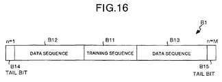
- Fig. 16 shows a burst B1 of received signals received during TDMA communications based on the conventional technology shown in Fig. 15.
- this burst B1 comprises a training sequence B11, data sequence B12, B13, and tail bits B14, B15, and the training sequence B11 and the tail bits B14, B15 are known in the receiver side.
- the CIR estimating circuit 211 computes, when having received a received signal r n , CIR estimated values g 0 , g 1 , ..., g L according to the training sequence B11 in the received burst B1 as shown in Fig. 16 as well as to the training sequence having previously been known in the receiver side.
- the phase deviation detecting circuit 212 first computes a phase deviation ⁇ m with the following equation according to the CIR estimated values g 0 , g 1 , ..., g L estimated with the known training sequence in the received burst B1 by the CIR estimating circuit 211 as well as to the known tail bits I n-L , I n-L+1 , ..., I n . It should be noted that a subscript m in the equation indicates a phase deviation in the burst of a m-th received signal.
- L indicates, as shown in the channel model in Fig. 14, a time length affected by intersymbol interference (ISI), namely a channel memory length, and corresponds to the number of stages in the delay circuit DELAY.
- ISI intersymbol interference
- s n is a replica (estimated value) of a received signal, at Re[a] a real part of a complex number a, at Im[a] an imaginary part of the complex number a, and at ABS[a] an absolute value of the complex number a respectively.
- phase deviation detecting circuit 212 computes a phase deviation per symbol ⁇ ⁇ m through the following equation according to the phase deviation ⁇ m as described above, and outputs a result of the computing to the averaging circuit 213.
- ⁇ ⁇ m ⁇ m ⁇ 2/(M - 1) ⁇ wherein M indicates a total number of symbols of a received burst B1.
- the averaging circuit 213 averages the phase deviation per symbol ⁇ ⁇ m estimated for each burst B1, and outputs a result of averaging to the frequency offset correcting circuit 214 as a frequency-offset estimated value ⁇ ⁇ m .
- the equalizer 215 determines data according to the received signal r' n having been subjected to offset correction outputted from the frequency offset correcting circuit 214 as well as to the CIR estimated value outputted from the CIR estimating circuit 211, and outputs a result of the decision as a decision value.
- tail bits other than the training sequence is required to compute a frequency-offset estimated value
- a length of tail bits in a received signal is generally required to be longer than a memory length L of the channel, so that transmission efficiency is worse in turn by the length required for the tail bits.
- a phase deviation is computed according to the CIR estimated value, the tail bits in the received signal and the estimated value (replica) of the bits, so that the phase deviation to be detected largely varies with noises. Accordingly, in order to estimate frequency offset with sufficient precision, it is required to suppress variation by making a time constant larger for averaging phase deviations, and for this reason, when frequency offset varies with time, it is difficult to follow the variation in the method described above.
- an error rate in decision is higher as compared to the case where diversity reception is performed.
- the present invention has been made for solving the problems as described above, and it is an object of the present invention to provide a receiver with a frequency offset correcting function which has improved the capabilities of being excellent in transmission efficiency without requiring known data other than a training sequence, precisely estimating time-varying frequency offset, and further enabling performance of diversity reception and determination of data at a low error rate.
- the present invention comprises a frequency offset correcting means for receiving a received signal as well as a frequency-offset estimated value and correcting phase rotation due to frequency offset of the received signal according to the frequency-offset estimated value; a first channel impulse response estimating means for estimating channel impulse response at a first position of the corrected received signal according to a known training sequence included in the received signal corrected by the frequency offset correcting means; a determining means for determining the received signal corrected by the frequency offset correcting means according to the channel impulse response estimated value at the first position thereof estimated by the first channel impulse response estimating means; a second channel impulse response estimating means for estimating channel impulse response at a second position apart from the first position of the corrected received signal according to the received signal corrected by the frequency offset correcting means, the channel impulse response estimated value at the first position thereof estimated by the first channel impulse response estimating means, and to the value determined by the determining means; and a frequency-offset estimated value computing means for computing a frequency-offset estimated value of the received signal according to the channel impulse impulse
- different channel-impulse estimated values at the first and second positions are obtained according to the training sequence having been known in the received signal, and a frequency-offset estimated value is computed according to those phase deviations, so that frequency offset of a received signal can be corrected and also data can be determined without using known data such as tail bits other than the training sequence.
- tail bits are not needed as a burst structure of a received signal, so that transmission efficiency is improved, and also a phase deviation can be computed not according to an estimated value (replica) of the received signal computed only with tail bits in a transmission sequence but according to channel impulse response estimated by sufficiently suppressing a noise element with an appropriate algorithm (e.g., LMS algorithm), and for this reason a phase deviation to be detected does not largely varies with noises, time-varying frequency offset can be compensated with high precision, and data can be determined at a low error rate.
- an appropriate algorithm e.g., LMS algorithm
- the another present invention comprises a frequency offset correcting means for receiving a received signal as well as a frequency-offset estimated value and correcting phase rotation due to frequency offset of the received signal according to the frequency-offset estimated value; a first channel impulse response estimating means for estimating channel impulse response at a first position of the corrected received signal according to a known training sequence included in the received signal corrected by the frequency offset correcting means; a determining means for determining the received signal corrected by the frequency offset correcting means; a second channel impulse response estimating means for estimating channel impulse response at a second position apart from the first position of the corrected received signal by updating the channel impulse response estimated value at the first position according to the received signal corrected by the frequency offset correcting means, the channel impulse response estimated value at the first position thereof estimated by the first channel impulse response estimating means, and to the value determined by the determining means; and a frequency-offset estimated value computing means for computing a frequency-offset estimated value of the received signal according to the channel impulse response estimated value at the first position thereof estimated by the first channel impulse response estimating
- determination of the received signal after the second time and on is made according to values obtained, by successively updating the channel impulse response estimated value at the first position, outputted from the second estimating means, so that, even when the channel impulse response estimated value varies with time, the variation can be followed, and data can be determined at a low error rate.
- the another present invention comprises a first channel impulse response estimating means for estimating channel impulse response at a first position of the received signal according to a known training sequence included in the received signal; a determining means for determining the received signal corrected by the frequency offset correcting means according to the channel impulse response estimated value at the first position thereof estimated by the first channel impulse response estimating means; a second channel impulse response estimating means for estimating channel impulse response at a second position apart from the first position of the received signal according to the received signal corrected by the frequency offset correcting means, the channel impulse response estimated value at the first position thereof estimated by the first channel impulse response estimating means, and to the value determined by the determining means; a frequency-offset estimated value computing means for computing a frequency-offset estimated value of the received signal according to the channel impulse response estimated value at the first position thereof estimated by the first channel impulse response estimating means as well as to the channel impulse response estimated value at the second position thereof estimated by the second channel impulse response estimating means; and a local oscillator correcting means for correcting a frequency from a local
- the another present invention comprises a frequency offset correcting means for receiving a plurality of received signals as well as frequency-offset estimated value, and correcting each phase rotation due to frequency offset for the plurality of received signals according to the frequency-offset estimated value respectively; a first channel impulse response estimating means for estimating each channel impulse response at a first position of the plurality of corrected received signals according to each known training sequence included in the plurality of received signals corrected by the frequency offset correcting means; a determining means for determining the plurality of received signals corrected by the frequency offset correcting means according to the channel impulse response estimated values each at the first position thereof estimated by the first channel impulse response estimating means; a second channel impulse response estimating means for estimating each channel impulse response at a second position apart from the first position of the plurality of corrected received signals according to the plurality of received signals corrected by the frequency offset correcting means, each channel impulse response estimated value at the first position of the plurality of corrected received signals estimated by the first channel impulse response estimating means, and to the value of the plurality of received signals determined by the determining
- the frequency-offset estimated value computing means comprises a phase deviation detecting means for detecting a phase deviation between the first position and the second position according to the channel impulse response estimated value at the first position estimated by the first channel impulse response estimating means as well as to the channel impulse response estimated value at the second position estimated by the second channel impulse response estimating means; and an averaging means for averaging phase deviations obtained by computing a phase deviation per symbol according to the phase deviation between the first position and the second position detected by the phase deviation detecting means to compute a frequency-offset estimated value, and outputting the computed value to the frequency offset correcting circuit.
- the phase deviation detecting means selects a value of which the absolute value is the maximum among the channel impulse response estimated values at the first position estimated by the first channel impulse response estimating means, and also selects a value corresponding to the channel impulse response estimated value at the first position of which the absolute value is the maximum among the channel impulse response estimated values at the second position estimated by the second channel impulse response estimating means; and detects a phase deviation of the received signal according to the product of complex conjugate of the channel impulse response estimated value at the first position of which the absolute value is the maximum and the channel impulse response estimated value at the second position corresponding to the channel impulse response estimated value at the first position of which the absolute value is the maximum.
- the phase deviation detecting means computes each product of the complex conjugate of the channel impulse response estimated value at the first position estimated by the first channel impulse response estimating means and the channel impulse response estimated value at the second position estimated by the second channel impulse response estimating means, and detects a phase deviation of the received signal according to the sum of the products each of which the absolute value is more than a threshold value among the computed products.
- the phase deviation detecting means computes each product of the complex conjugate of the channel impulse response estimated value at the first position estimated by the first channel impulse response estimating means and the channel impulse response estimated value at the second position estimated by the second channel impulse response estimating means, selects each product of which the absolute value is more than a threshold value among the computed products, multiplies each of the absolute values to the selected products, and detects the phase deviation of the received signals according to the sum of the multiplied values.
- phase deviation detecting means further quantizes the phase deviation of the detected received signal, and outputs a result of the quantization as a phase deviation.
- the determining means comprises a soft-decision equalizer for executing soft-decision of a data sequence in the corrected received signal according to the received signal corrected by the frequency offset correcting means as well as to the channel impulse response estimated value at the first position estimated by the first channel impulse response estimating means; and a hard-decision circuit for executing hard decision of the soft-decision value estimated by the soft-decision equalizer and outputting a result of the decision as a decision value of a data sequence in the received signal. Therefore, with this invention, decision can be made including reliability by the soft-decision equalizer, so that the reliability can be utilized in forward error correction and so on.
- Fig. 1 is a block diagram showing configuration of a receiver with a frequency offset correcting function according to Embodiment 1 of the present invention
- Fig. 2 is a view showing a burst structure of the received signal in Embodiment 1
- Fig. 3 is a view showing configuration of a determining circuit 13a having an equalizer for executing soft-determination in place of equalizer 13
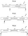
- Fig. 4 is a view showing another method of computing a CIR estimated value at the second position
- Fig. 5 is a view showing another method of computing a CIR estimated value at the second position
- Fig. 6 is a view showing another method of computing a CIR estimated value at the second position
- Fig. 1 is a block diagram showing configuration of a receiver with a frequency offset correcting function according to Embodiment 1 of the present invention
- Fig. 2 is a view showing a burst structure of the received signal in Embodiment 1
- Fig. 3 is a view showing configuration of a determining circuit
- FIG. 7 is a view showing another method of computing a CIR estimated value at the second position
- Fig. 8 is a view showing another method of computing a CIR estimated value at the second position
- Fig. 9 is a view showing another method of computing a CIR estimated value at the second position
- Fig. 10 is a view showing a graph of a quantizing function
- Fig. 11 is a block diagram showing configuration of a receiver with a frequency offset correcting function according to Embodiment 2 of the present invention
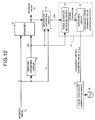
- Fig. 12 is a block diagram showing configuration of a receiver with a frequency offset correcting function according to Embodiment 3 of the present invention
- FIG. 13 is a block diagram showing configuration of a receiver with a frequency offset correcting function according to Embodiment 4 of the present invention
- Fig. 14 is a block diagram showing a model of a channel with intersymbol interference (ISI) therein
- Fig. 15 is a block diagram showing configuration of the receiver with a frequency offset correcting function based on the conventional technology
- Fig. 16 is a view showing a burst structure of a received signal in the example based on the conventional technology.
- ISI intersymbol interference
- Fig. 1 is a block diagram showing configuration of the receiver with the frequency offset correcting function according to Embodiment 1 of the present invention.
- a frequency offset correcting circuit for correcting a received signal r n with a frequency-offset estimated value ⁇ ⁇ m outputted from an averaging circuit 16 described later;
- a first CIR estimating circuit for estimating CIR at a first position on a burst according to a training sequence in a received signal r' n corrected by the frequency offset correcting circuit 11;
- an equalizer as a determining means for equalizing a data sequence in the received signal according to the received signal r' n corrected by the frequency offset correcting circuit 11 as well as to the CIR estimated value at the first position estimated by the first CIR estimating circuit 12, and determining, when a binary signal of, for instance, 1 or -1 is received, which value of 1 and -1 is the received signal r n or the like;
- a second CIR estimating circuit for estimating a CIR estimated value at a second position apart from the first position on the burst in a corrected received signal r
- Fig. 2 shows a burst B2 of the received signal r n in
- the burst B2 of the received signal r n in Embodiment 1 comprises a training sequence B21 known in the receiver and data sequence B22, and does not include tail bits different from the burst B1 having been described in the conventional technology shown in Fig. 16.
- n is a time, at P1 a time M1, namely a first position indicating a symbol of the time corresponding to a final symbol of the training sequence B21 in the burst B2, at P2 a second position indicating a symbol of a time M2, and M0 is a time indicating a length of all the symbols in this burst B2.
- the burst B2 may also include tail bits similarly to the case of the burst B1 based on the conventional technology, but the present invention has eliminated the need for tail bits because frequency offset of a received signal is computed and corrected only based on the training sequence without using the tail bits.
- the frequency offset correcting circuit 11 corrects a received signal r n at a time m-1 one time interval before the time m as described later based on the frequency-offset estimated value ⁇ ⁇ m-1 having been estimated by the averaging circuit 16 through the following equation.
- r' n r n exp (-j ⁇ ⁇ m-1 n)
- the first CIR estimating circuit 12 computes CIR estimated values g 0, n , g 1, n , ..., g L, n with an LMS (Least Mean Square) algorithm according to the known training sequence I n as well as to the training sequence B21 in the corrected received signal r' n .
- LMS Least Mean Square
- the reference sign ⁇ indicates a step size of the LMS algorithm, and initial values g 0, L , g 1, L , ..., g L, L of the CIR estimated values are set to arbitrary values respectively.
- the reference sign L indicates, as described in the conventional technology, a time length affected by intersymbol interference (ISI) in the transmission model in Fig. 14, namely a channel memory length.
- the reference sign M1 indicates a time corresponding to the final symbol of the training sequence in the burst B2 and is a first position where the first CIR is estimated.
- the equalizer 13 determines a data sequence according to the CIR estimated values g 0, M1 , g 1, M1 , ..., g L, M1 outputted from the first CIR estimating circuit 12 as well as to the corrected received signal r' n , and outputs a result of the decision as a decision value J n .
- the decision value J n indicates not a decision value outputted at the time n but a decision value corresponding to the transmitted signal I n . Namely, J n will be equal to I n on condition that appropriate decision is made.
- the second CIR estimating circuit 14 updates the CIR estimated values g 0, n , g 1, n , ..., g L, n with the LMS algorithm according to the corrected received signal r' n as well as to the decision value J n outputted from the equalizer 13 with the CIR estimated values g 0, M1 , g 1, M1 , ..., g L, M1 , as initial values, at the first position P1 in the burst B2 outputted from the first CIR estimating circuit 12, namely at the time M1 corresponding to the final symbol of the training sequence B21 in the burst B2 as shown in Fig.
- the phase deviation detecting circuit 15 detects, when having received a CIR estimated value at the second position P2 from the second CIR estimating circuit 14, a phase deviation according to the sequence described below.
- any CIR estimated value of which the absolute value is maximum is selected as a tap coefficient among the CIR estimated values g 0, M1 , g 1, M1 , ..., g L, M1 at the first position on the burst B2 outputted from the first CIR estimating circuit 12.
- a CIR estimated value of which the absolute value is maximum is a tap coefficient g Max, M1 .
- the averaging circuit 16 divides the phase deviation ⁇ m outputted from the phase deviation detecting circuit 15 by (M2 - M1) to compute the phase deviation ⁇ ⁇ m per symbol.
- ⁇ ⁇ m ⁇ m /(M2 - M1)
- the frequency offset correcting circuit 11 corrects a received signal r n to be inputted according to a frequency-offset estimated value ⁇ ⁇ m from the averaging circuit 16 through the equation (9).
- frequency offset is estimated without using known data such as tail bits other than the training sequence, and data can be determined while distortion of the frequency offset is compensated, so that the need for the known data such as tail bits other than the training sequence can be eliminated, transmission efficiency can be improved, and there is no need for suppressing variation by making a time constant larger for averaging a phase deviation to estimate frequency offset with sufficient precision, and for this reason, even when frequency offset varies with time, the variation can easily be followed, and time-varying frequency offset can be estimated with high precision.
- a phase deviation is detected based on a CIR estimated value at the first position P1 estimated according to the known training sequence and a training sequence in a received signal as well as on a CIR estimated value at the second position P2 apart from the first position obtained by updating this CIR estimated value at the first position with the LMS algorithm, so that, by making a step size of the LMS algorithm smaller, CIR estimated values at both of the first position and the second position in which noise elements included in the received signal are sufficiently suppressed can be obtained, and frequency offset can be corrected with frequency-offset estimated values having less noise element.
- Embodiment 1 a phase deviation can precisely be detected, which allows a time constant for averaging to be made smaller and time-varying frequency offset to be estimated with high precision.
- equalizer 13 a non-linear equalizer and a linear equalizer such as a decision-feedback equalizer may be used.
- a RLS (Recursive Least Squares) algorithm and modified algorithms of the LMS algorithm and the RLS algorithm may be used for updating of the CIR estimated values by the second estimating circuit 14.
- phase deviation ⁇ ⁇ m per symbol is computed in the averaging circuit 16
- a computing method can also be changed so that the phase deviation ⁇ ⁇ m per symbol is computed in the phase deviation detecting circuit 15 like in the conventional technology.
- the computing method can also be changed so that a frequency-offset estimated value ⁇ ⁇ m is computed by averaging a phase deviation ⁇ m in the averaging circuit 16 and dividing a result of the averaging by (M2-M1).
- a decision circuit 13a comprising a combination of a soft-decision equalizer 13a1 for outputting soft-decision value with a hard-decision circuit 13a2 for hard-decision a soft-decision value described in "Optimum and sub-optimum detection of coded data distributed by time-varying intersymbol interference (IEEE GLOBECOM' 90, San Diego, pp. 1679-1685, Dec. 1990) by W. Koch et al. or the like may be provided.
- the equalizer 13 in Embodiment 1 determines which of 1 and -1 is transmitted from a received signal, what is called, makes hard decision, while the soft-decision equalizer 13a1 determines received signals by assigning weights to received signals including reliability of the received signals, namely depending on the reliability of the received signals, and a result of the decision is outputted at multivalues such as 1.2, 0.3, and -0.5.
- the hard-decision circuit 13a2 makes hard-decision, namely determines which of 1 and -1 the transmitted signal is in the case described above according to the decision output from the soft-decision equalizer 13a1 and outputs a decision value J n .
- a CIR estimated value at the second arbitrary position P2 in the data sequence B32 may be computed through the same processing as that in Embodiment 1 by obtaining a CIR estimated value at a first arbitrary position in the data sequence B33 by means of the same processing as that in Embodiment 1 according to the CIR estimated value at the time of the final symbol in the training sequence B31 and reversing the series on its time axis according to the CIR estimated value at the time of a header symbol in the training sequence B31.
- a phase deviation may also be computed by using only the training sequence B31 and data sequence B33 with the CIR estimated value at the first position which is a time corresponding to the final symbol of the training sequence B31 as well as with the CIR estimated value at the second arbitrary position of the training sequence B31 by means of the same processing as that in Embodiment 1 shown in Fig. 2.
- a position of the final symbol in the data sequence B33 is regarded as the first position P1 and a CIR estimated value maybe computed at the position through the same processing as that in Fig. 3, and also for the training sequence B31 and data sequence B32, a position of the header symbol in the data sequence B32 is also regarded as the second position P2 and a CIR estimated value may be computed through the same processing as that in Fig. 3 by reversing the sequence on its time axis.
- a phase deviation may also be computed by using only the training sequence B31 and data sequence B33 through the same processing as the method described in Embodiment 1 shown in Fig. 2 and the method shown in Fig. 4.
- CIR estimated values for instance, at the plurality of positions P21 to P24 in the data sequence B33 are obtained and CIR estimated values, for instance, at the plurality of positions P21' to P24' in the data sequence B31 are obtained by regarding the header or the tail of the training sequence B32 as each of the first positions P1 and P1' and based on the CIR estimated values at the positions, a plurality of phase deviations are obtained from the CIR estimated values at the adjacent position to each other, the plurality of phase deviations are averaged, and the averaged value may be outputted to the averaging circuit 16 as a phase deviation.
- a CIR estimated value at the position P1 of the known training sequence B41 is obtained similarly to the case in Embodiment 1 shown in Fig. 2, CIR estimated values at a plurality of positions such as positions P2 to P5 are computed based on the CIR estimated value at the first position P1, a plurality of phase deviations are obtained from the CIR estimated values at adjacent positions to each other, the plurality of phase deviations are averaged, and the average value may be outputted to the averaging circuit 16 as a phase deviation.
- phase deviation detecting circuit 15 may detect a phase deviation according to the method as described below.
- the phase deviation detecting circuit 15 according to Embodiment 1 may detect a phase deviation according to the method as described below.
- phase deviations ⁇ i, m each in which ABS[ ⁇ i, m ] as absolute values of the phase deviation ⁇ i, m is more than a specified threshold value are selected, and the sum by assigning weights to the phase deviations with the absolute values ABS[ ⁇ i, m ] is a phase deviation ⁇ COM, m on the complex plane as shown in the following equation. With those operations, weights are assigned to the phase deviations ⁇ i, m with the absolute values ABS [ ⁇ i, m ] thereof, so that a more accurate phase deviation can be obtained.
- phase deviation detecting circuit 15 quantizes a phase deviation ⁇ m with a function in which a quantized phase deviation q m is changed step by step according to changes for each specified rate of the phase deviation ⁇ m as shown in Fig. 10, and may also output a result of quantization to the averaging circuit 16 in place of the phase deviation ⁇ m as a quantized phase deviation q m .
- an IIR filter a random walk filter or an N-Before-M filter other than the FIR filter can be used for averaging in the averaging circuit 16.
- the averaging circuit 16 outputs control data for correction of frequency offset in place of outputting a frequency-offset estimated value, and can correct the frequency offset of the received signal in the frequency offset correcting circuit 11 based on the control data.
- the RLS algorithm and modified algorithms of the LMS algorithm and the RLS algorithm may be used. Further, a CIR estimated value can be computed based on a correlation between a training sequence and a training sequence in the received signal. However, when computing is carried out by using the correlation, the CIR estimated value computed with the training sequence is a value at the center of the training sequence.
- Embodiment 1 may be realized with firmware such as DSP, hardware software.
- Fig. 11 shows configuration of the receiver with a frequency offset correcting function according to Embodiment 2. It should be noted that, in the figure, the same reference numerals are assigned to the components corresponding to those in Embodiment 1 shown in Fig. 1.
- Embodiment 2 is characterized in that an equalizer 13b is provided for determining a received signal r' n of which the frequency offset has been corrected according to a CIR estimated value at the first position from the first CIR estimating circuit 12 as well as to an updated value of the CIR estimated value at the first position outputted from the second CIR estimating circuit 14b in place of the equalizer 13 according to Embodiment 1 for determining a received signal r' n of which the frequency offset has been corrected from the frequency offset correcting circuit according to a CIR estimated value at the first position from the first CIR estimating circuit 12.
- the second CIR estimating circuit 14b is so configured as to successively update, when a CIR estimated value at the second position is to be estimated, a CIR estimated value at the first position as shown in the equation (11) based on the time n and successively output the updated values to a equalizer 13b.
- this equalizer 13b does not receive an updated value of a CIR estimated value only for the first time from a second CIR estimating circuit 14b, so that the equalizer 13b equalizes a received signal r' n corrected by the frequency offset correcting circuit 11 according to the CIR estimated values g i, M1 outputted from the first CIR estimating circuit 12, and determines a data sequence in the received signal.
- the equalizer 13 determines a received signal r' n corrected by the frequency offset correcting circuit 11 according to the CIR estimated values g i, n (n M1+1, ..., M2) successively updated and outputted from the second CIR estimating circuit 14.
- the equalizer 13b determines a data sequence of the transmitted signal, received signals after the second time and on are determined based on successively updated values of the CIR estimated values at the first position successively outputted from the second CIR estimating circuit 14b, so that even when the CIR estimated values varies with time, the variation can be followed, and data can be made decision at a low error rate.
- Fig. 12 shows configuration of the receiver with a frequency offset correcting function according to Embodiment 3. It should be noted that, in the figure, the same reference numerals are assigned to the components corresponding to those in Embodiment 1 shown in Fig. 1.
- Embodiment 3 is characterized in that a local oscillator correcting circuit 19 is provided for correcting a frequency from a local oscillator 18 of the receiver with a frequency-offset estimated value outputted from the averaging circuit 16 in place of correcting frequency offset of the received signal in the frequency offset correcting circuit 11. For this reason, with Embodiment 3, the same effect as that of Embodiment 1 can be obtained.
- Fig. 13 is a block diagram showing an example of the receiver with a frequency offset correcting function according to Embodiment 2.
- P-units of frequency offset correcting circuits for receiving received signals r n,1 to r n, p and correcting the received signals r n,1 to r n, p based on frequency offset estimated values ⁇ ⁇ m respectively;
- a first CIR estimating circuit for estimating CIR at the first position on a burst according to a training sequence in P-pieces of received signals r' n, 1 to r' n, p corrected by the P-units of frequency offset correcting circuit 21 respectively;
- an equalizer for estimating data sequence in the received signals according to the received signals r' n, 1 to r' n, p corrected by the frequency offset correcting circuits 211 to 21P as well as to each CIR estimated value at the first position estimated by the first CIR estimating circuit 22, and estimating, when a binary signal, for instance, 1 or -1 is transmitted, which value of
- a received signal comprises the burst B2 shown in Fig. 2 described in Embodiment 1, namely the training sequence B21 and the data sequence B22, and it is assumed that the burst B2 of which the training sequence B21 has been known by the receiver is received.
- the frequency offset correcting circuits 211 to 22P correct P-pieces of received signals r n, p respectively based on frequency-offset estimated values ⁇ ⁇ m-1 through the following equation.
- r' s r n, p exp(-j ⁇ ⁇ m-1 n)
- the first CIR estimating circuit 22 computes CIR estimated values g 0, n, p , g 1, n, p , ..., g L, n, p with the LMS algorithm according to each known training sequence I n as well as to each training sequence in the corrected P-pieces of received signals r' n, p .
- the reference sign ⁇ indicates a step size of the LMS algorithm, and initial values g 0, L, p , g 1, L, p , ..., g L, L, p of the CIR estimated values are set to arbitrary values respectively. It should be noted that the reference sign M1 indicates a time corresponding to the final symbol of the training sequence.
- the equalizer 23 determines a data sequence according to the CIR estimated values g 0, M1, p , g 1, M1, p , ..., g L, M1, p for P-pieces of received signal r' n, p corrected and outputted from the first CIR estimating circuit 22 as well as to the corrected P-pieces of received signal r' n, p and outputs a result of the decision as a decision value J n .
- the second CIR estimating circuit 24 updates the CIR estimated values g 0, n, p , g 1, n, p , ..., g L, n, p with the LMS algorithm according to the corrected received signals r' n, p as well as to the decision value J n outputted from the equalizer 23 with the CIR estimated values g 0, M1, p , g 1, M1, p , ... g L, M1, p outputted from the first CIR estimating circuit 22 as initial values.
- a training sequence I n is used in place of a decision value J n .
- the phase deviation detecting circuit 25 detects a phase deviation according to the series described below.
- any CIR estimated value of which the absolute value is maximum is selected as a tap coefficient among the CIR estimated values g 0, M1, p , g 1, M1, p , ..., g L, M1, p outputted from the first CIR estimating circuit 22.
- a CIR estimated value of which the absolute value is maximum is a tap coefficient g Max, M1 .
- a* indicates a complex conjugate of a complex number a.
- the averaging circuit 26 divides the phase deviation ⁇ m outputted from the phase deviation detecting circuit 25 by (M2 - M1) to compute the phase deviation ⁇ ⁇ m per symbol.
- ⁇ ⁇ m ⁇ m /(M2 - M1)
- the averaging circuit 26 averages the phase deviation ⁇ ⁇ m per symbol with a FIR filter expressed with the following equation, and outputs a result of the averaging as each frequency-offset estimated value ⁇ ⁇ m to the frequency offset correcting circuits 211 to 21P.
- each of the P-units of frequency offset correcting circuits 211 to 21P corrects each of received signals r n, p based on the frequency-offset estimated value ⁇ ⁇ m from the averaging circuit 16 through the equation (23) respectively.
- frequency offset is estimated without using known data such as tail bits other than the training sequence, and data can be determined while distortion of the frequency offset is compensated, so that, similarly to the case of Embodiment 1, the need for the known data such as tail bits other than the training sequence can be eliminated, transmission efficiency can be improved, even when frequency offset varies with time, the variation can be followed, time-varying frequency offset can be estimated with high precision, and further frequency offset can be corrected with a frequency-offset estimated value with less noise element.
- a plurality of frequency offset correcting circuits 211 to 21P are provided, and each data sequence for a plurality of received signals r n, p is determined with the equalizer 23, so that diversity reception can be realized and a error rate of determined data can be reduced.
- CIR estimated values at first and second positions are obtained according to a known training sequence in a received signal, and a frequency-offset estimated value can be computed according to those phase deviations, so that frequency offset of the received signal can be corrected without using known data such as tail bits other than the training sequence, and data in the received signal can be determined.
- determination of received signals at the second time and thereafter in a determining means can be made based on values, obtained by successively updating a CIR estimated value at the first position, outputted from the second estimating means, so that even when the CIR estimated value varies with time, determination can follow the variations, which allows data to be determined at a low error rate.
- decision including reliability is made with a soft-decision equalizer, which allows the reliability to be utilized in forward error correction and so on.
Landscapes
- Engineering & Computer Science (AREA)
- Computer Networks & Wireless Communication (AREA)
- Signal Processing (AREA)
- Power Engineering (AREA)
- Digital Transmission Methods That Use Modulated Carrier Waves (AREA)
- Cable Transmission Systems, Equalization Of Radio And Reduction Of Echo (AREA)
Applications Claiming Priority (4)
| Application Number | Priority Date | Filing Date | Title |
|---|---|---|---|
| CNB971943796A CN1158786C (zh) | 1997-03-04 | 1997-03-04 | 带频率偏移校正功能的接收机 |
| PCT/JP1997/000653 WO1998039854A1 (fr) | 1997-03-04 | 1997-03-04 | Recepteur avec fonction de correction du decalage de frequence |
| CA002251921A CA2251921C (fr) | 1997-03-04 | 1997-03-04 | Recepteur avec fonction de correction du decalage de frequence |
| US09/185,744 US6347126B1 (en) | 1997-03-04 | 1998-11-04 | Receiver with a frequency offset correcting function |
Publications (2)
| Publication Number | Publication Date |
|---|---|
| EP0959568A1 true EP0959568A1 (fr) | 1999-11-24 |
| EP0959568A4 EP0959568A4 (fr) | 2007-09-26 |
Family
ID=27427486
Family Applications (1)
| Application Number | Title | Priority Date | Filing Date |
|---|---|---|---|
| EP97905438A Withdrawn EP0959568A4 (fr) | 1997-03-04 | 1997-03-04 | Recepteur avec fonction de correction du decalage de frequence |
Country Status (6)
| Country | Link |
|---|---|
| US (1) | US6347126B1 (fr) |
| EP (1) | EP0959568A4 (fr) |
| CN (1) | CN1158786C (fr) |
| AU (1) | AU723679B2 (fr) |
| CA (1) | CA2251921C (fr) |
| WO (1) | WO1998039854A1 (fr) |
Cited By (12)
| Publication number | Priority date | Publication date | Assignee | Title |
|---|---|---|---|---|
| FR2805690A1 (fr) * | 2000-02-25 | 2001-08-31 | Nortel Matra Cellular | Procede d'estimation d'un ecart de frequence radio, et recepteur de radiocommunication mettant en oeuvre le procede |
| WO2001045253A3 (fr) * | 1999-12-17 | 2001-12-13 | Infineon Technologies Ag | Circuit et procede pour la compensation de decalage d'un signal |
| WO2005064874A1 (fr) * | 2003-12-30 | 2005-07-14 | Nokia Corporation | Commande de frequence pour un dispositif de communication mobile |
| US7020492B2 (en) | 2000-04-03 | 2006-03-28 | Sanyo Electric Co., Ltd. | Radio |
| US7035358B1 (en) * | 2001-02-23 | 2006-04-25 | Arraycomm, Inc. | Method and apparatus for receiving a wideband signal in the presence of multipath channel imperfections and frequency offset |
| EP1320232A3 (fr) * | 2001-12-12 | 2006-07-19 | Texas Instruments Incorporated | Estimation et correction de phase dans des système MDFO |
| WO2006094140A1 (fr) * | 2005-03-01 | 2006-09-08 | Qualcomm Incorporated | Commande de frequence automatique a double boucle pour communication sans fil |
| EP1225739A4 (fr) * | 2000-07-31 | 2009-03-25 | Mitsubishi Electric Corp | Recepteur de radiocommunication |
| WO2010072263A1 (fr) * | 2008-12-23 | 2010-07-01 | Telefonaktiebolaget L M Ericsson (Publ) | Procédé et appareil pour la compensation d'erreur de fréquence de récepteur |
| US8009775B2 (en) | 2005-03-11 | 2011-08-30 | Qualcomm Incorporated | Automatic frequency control for a wireless communication system with multiple subcarriers |
| US8433005B2 (en) | 2004-01-28 | 2013-04-30 | Qualcomm Incorporated | Frame synchronization and initial symbol timing acquisition system and method |
| US8724447B2 (en) | 2004-01-28 | 2014-05-13 | Qualcomm Incorporated | Timing estimation in an OFDM receiver |
Families Citing this family (41)
| Publication number | Priority date | Publication date | Assignee | Title |
|---|---|---|---|---|
| AU724387B2 (en) * | 1997-02-04 | 2000-09-21 | Nokia Telecommunications Oy | Compensation of doppler shift in a mobile communication system |
| US6208617B1 (en) * | 1998-02-27 | 2001-03-27 | Lucent Technologies, Inc. | Channel tracking in a mobile receiver |
| GB2339120B (en) * | 1998-06-30 | 2003-03-19 | Nec Technologies | Channel estimation device for digital telecommunications stations |
| DE19854167C2 (de) * | 1998-11-24 | 2000-09-28 | Siemens Ag | Frequenzstabilisierte Sende-/Empfangsschaltung |
| US6748026B1 (en) * | 1999-02-12 | 2004-06-08 | Matsushita Electric Industrial Co., Ltd. | Distortion estimation apparatus, frequency offset compensation apparatus and reception apparatus |
| JP3344353B2 (ja) * | 1999-03-16 | 2002-11-11 | 日本電気株式会社 | 位相同期ループ回路と受信システム |
| JP3859903B2 (ja) | 1999-06-10 | 2006-12-20 | 三菱電機株式会社 | 周波数誤差推定装置およびその方法 |
| US6674815B2 (en) * | 1999-06-16 | 2004-01-06 | Ericsson, Inc | Method for symbol-spaced estimation and/or tracking of a fractionally-spaced fading radio channel |
| JP3190318B2 (ja) * | 1999-07-07 | 2001-07-23 | 三菱電機株式会社 | 周波数誤差推定装置および周波数誤差推定方法 |
| US6463266B1 (en) * | 1999-08-10 | 2002-10-08 | Broadcom Corporation | Radio frequency control for communications systems |
| JP3544643B2 (ja) * | 2000-07-14 | 2004-07-21 | 松下電器産業株式会社 | チャネル推定装置及びチャネル推定方法 |
| DE10043743A1 (de) * | 2000-09-05 | 2002-03-14 | Infineon Technologies Ag | Automatische Frequenzkorrektur für Mobilfunkempfänger |
| US6710644B2 (en) | 2000-11-29 | 2004-03-23 | Broadcom Corporation | Low pass filter corner frequency tuning circuit and method |
| US6993107B2 (en) * | 2001-01-16 | 2006-01-31 | International Business Machines Corporation | Analog unidirectional serial link architecture |
| GB2375272B (en) * | 2001-04-30 | 2003-11-19 | Lucent Technologies Inc | A frequency estimator for use in a receiver of packetised data, the receiver and a method of reception |
| US6690753B2 (en) * | 2001-06-08 | 2004-02-10 | Broadcom Corporation | Receiver having decisional feedback equalizer with remodulation and related methods |
| US7123670B2 (en) * | 2001-09-24 | 2006-10-17 | Atheros Communications, Inc. | Fine frequency offset estimation and calculation and use to improve communication system performance |
| GB0124952D0 (en) * | 2001-10-17 | 2001-12-05 | Nokia Corp | A receiver and a receiving method |
| US7020222B2 (en) * | 2001-10-24 | 2006-03-28 | Texas Instruments Incorporated | Efficient method and system for offset phasor determination |
| GB0126130D0 (en) * | 2001-10-31 | 2002-01-02 | Nokia Corp | Frequency error estimation |
| KR100916377B1 (ko) * | 2002-04-16 | 2009-09-07 | 톰슨 라이센싱 | 결정 피드백 등화기 및 결정 피드백 등화를 위한 방법 |
| AU2003226054A1 (en) * | 2002-04-17 | 2003-11-03 | Seo Weon Heo | Equalizer mode switch |
| US7277504B2 (en) * | 2002-06-27 | 2007-10-02 | Telefonktiebolaget Lm Ericsson (Publ) | Method and system for concurrent estimation of frequency offset and modulation index |
| US7245672B2 (en) * | 2002-06-27 | 2007-07-17 | Telefonaktiebolaget Lm Ericsson (Publ) | Method and apparatus for phase-domain semi-coherent demodulation |
| US7209177B2 (en) * | 2002-09-03 | 2007-04-24 | Audisoft | Headset for camera |
| US6697016B1 (en) * | 2002-09-30 | 2004-02-24 | Motorola, Inc. | Self adjustment of a frequency offset in a GPS receiver |
| JP4057471B2 (ja) * | 2003-06-06 | 2008-03-05 | 日本電信電話株式会社 | 搬送波同期回路 |
| EP1508983B1 (fr) * | 2003-08-18 | 2005-12-14 | Alcatel | Méthode de transmission optique et récepteur optique |
| JP4346465B2 (ja) * | 2003-09-29 | 2009-10-21 | 三洋電機株式会社 | 受信方法および装置 |
| KR20050040615A (ko) * | 2003-10-29 | 2005-05-03 | 삼성전자주식회사 | 훈련열 데이터를 이용하여 채널을 추정하는 디지털수신기를 위한 채널 추정 장치 및 그 방법 |
| US7502412B2 (en) * | 2004-05-20 | 2009-03-10 | Qisda Corporation | Adaptive channel estimation using decision feedback |
| US7535976B2 (en) * | 2004-07-30 | 2009-05-19 | Broadcom Corporation | Apparatus and method for integration of tuner functions in a digital receiver |
| US7154346B2 (en) * | 2004-07-30 | 2006-12-26 | Broadcom Corporation | Apparatus and method to provide a local oscillator signal |
| DE102004052898B4 (de) * | 2004-11-02 | 2009-10-29 | Infineon Technologies Ag | Kompensation des Trägerfrequenz-Offsets in einer für mehrere Modulationsarten ausgelegten Empfangsvorrichtung eines mobilen Kommunikationssystems |
| JP5115340B2 (ja) * | 2008-06-09 | 2013-01-09 | 富士通株式会社 | 無線通信装置および周波数偏差算出方法 |
| JP4796212B1 (ja) * | 2011-05-16 | 2011-10-19 | パナソニック株式会社 | 受信装置及び受信方法 |
| JP4796213B1 (ja) * | 2011-05-16 | 2011-10-19 | パナソニック株式会社 | 等化装置及び等化方法 |
| CN103986535B (zh) * | 2014-05-29 | 2015-12-30 | 国家电网公司 | 一种测试接收机可接受频率偏移的装置 |
| CN104571264A (zh) * | 2014-12-29 | 2015-04-29 | 大唐移动通信设备有限公司 | 一种时延调整方法和装置 |
| KR102025324B1 (ko) * | 2017-09-27 | 2019-09-25 | (주)에프씨아이 | 주파수 오프셋 추정 방법 |
| US11381281B2 (en) * | 2020-02-04 | 2022-07-05 | Powermat Technologies Ltd. | Fast data transmission for wireless power transfer systems |
Family Cites Families (8)
| Publication number | Priority date | Publication date | Assignee | Title |
|---|---|---|---|---|
| SE457399B (sv) | 1987-04-23 | 1988-12-19 | Ericsson Telefon Ab L M | Anordning i en koherrent mobiltelefonmottagare foer reducering av bitfel |
| IL92288A (en) * | 1988-12-16 | 1996-09-12 | Motorola Inc | Method and device for automatic frequency control |
| US5245611A (en) * | 1991-05-31 | 1993-09-14 | Motorola, Inc. | Method and apparatus for providing carrier frequency offset compensation in a tdma communication system |
| US5311545A (en) | 1991-06-17 | 1994-05-10 | Hughes Aircraft Company | Modem for fading digital channels affected by multipath |
| US5263026A (en) * | 1991-06-27 | 1993-11-16 | Hughes Aircraft Company | Maximum likelihood sequence estimation based equalization within a mobile digital cellular receiver |
| US5579345A (en) * | 1994-10-13 | 1996-11-26 | Westinghouse Electric Corporation | Carrier tracking loop for QPSK demodulator |
| JPH08223096A (ja) * | 1995-02-14 | 1996-08-30 | Kokusai Electric Co Ltd | 広帯域直交変調無線受信機 |
| US6151368A (en) * | 1999-03-22 | 2000-11-21 | Sicom, Inc. | Phase-noise compensated digital communication receiver and method therefor |
-
1997
- 1997-03-04 CN CNB971943796A patent/CN1158786C/zh not_active Expired - Fee Related
- 1997-03-04 EP EP97905438A patent/EP0959568A4/fr not_active Withdrawn
- 1997-03-04 WO PCT/JP1997/000653 patent/WO1998039854A1/fr not_active Ceased
- 1997-03-04 AU AU22314/97A patent/AU723679B2/en not_active Ceased
- 1997-03-04 CA CA002251921A patent/CA2251921C/fr not_active Expired - Fee Related
-
1998
- 1998-11-04 US US09/185,744 patent/US6347126B1/en not_active Expired - Fee Related
Cited By (19)
| Publication number | Priority date | Publication date | Assignee | Title |
|---|---|---|---|---|
| US6944220B2 (en) | 1999-12-17 | 2005-09-13 | Infineon Technologies Ag | Circuit configuration for the offset compensation of a signal |
| WO2001045253A3 (fr) * | 1999-12-17 | 2001-12-13 | Infineon Technologies Ag | Circuit et procede pour la compensation de decalage d'un signal |
| WO2001065792A1 (fr) * | 2000-02-25 | 2001-09-07 | Nortel Networks Limited | Procede d'estimation d'un ecart de frequence radio sur la base de sequences de symboles predefinis, et recepteur mettant en oeuvre le procede |
| FR2805690A1 (fr) * | 2000-02-25 | 2001-08-31 | Nortel Matra Cellular | Procede d'estimation d'un ecart de frequence radio, et recepteur de radiocommunication mettant en oeuvre le procede |
| EP1274180A4 (fr) * | 2000-04-03 | 2009-06-24 | Sanyo Electric Co | Radio |
| US7020492B2 (en) | 2000-04-03 | 2006-03-28 | Sanyo Electric Co., Ltd. | Radio |
| EP1225739A4 (fr) * | 2000-07-31 | 2009-03-25 | Mitsubishi Electric Corp | Recepteur de radiocommunication |
| US7035358B1 (en) * | 2001-02-23 | 2006-04-25 | Arraycomm, Inc. | Method and apparatus for receiving a wideband signal in the presence of multipath channel imperfections and frequency offset |
| EP1320232A3 (fr) * | 2001-12-12 | 2006-07-19 | Texas Instruments Incorporated | Estimation et correction de phase dans des système MDFO |
| US7180965B2 (en) | 2001-12-12 | 2007-02-20 | Texas Instruments Incorporated | Phase estimation and compensation in orthogonal frequency division multiplex (OFDM) systems |
| US7474718B2 (en) | 2003-12-30 | 2009-01-06 | Nokia Corporation | Frequency control for a mobile communications device |
| WO2005064874A1 (fr) * | 2003-12-30 | 2005-07-14 | Nokia Corporation | Commande de frequence pour un dispositif de communication mobile |
| US8433005B2 (en) | 2004-01-28 | 2013-04-30 | Qualcomm Incorporated | Frame synchronization and initial symbol timing acquisition system and method |
| US8724447B2 (en) | 2004-01-28 | 2014-05-13 | Qualcomm Incorporated | Timing estimation in an OFDM receiver |
| WO2006094140A1 (fr) * | 2005-03-01 | 2006-09-08 | Qualcomm Incorporated | Commande de frequence automatique a double boucle pour communication sans fil |
| US8401503B2 (en) | 2005-03-01 | 2013-03-19 | Qualcomm Incorporated | Dual-loop automatic frequency control for wireless communication |
| US8009775B2 (en) | 2005-03-11 | 2011-08-30 | Qualcomm Incorporated | Automatic frequency control for a wireless communication system with multiple subcarriers |
| WO2010072263A1 (fr) * | 2008-12-23 | 2010-07-01 | Telefonaktiebolaget L M Ericsson (Publ) | Procédé et appareil pour la compensation d'erreur de fréquence de récepteur |
| US9036750B2 (en) | 2008-12-23 | 2015-05-19 | Telefonaktiebolaget L M Ericsson (Publ) | Method and apparatus for receiver frequency error compensation |
Also Published As
| Publication number | Publication date |
|---|---|
| CA2251921A1 (fr) | 1998-09-11 |
| EP0959568A4 (fr) | 2007-09-26 |
| CA2251921C (fr) | 2003-07-08 |
| CN1217839A (zh) | 1999-05-26 |
| CN1158786C (zh) | 2004-07-21 |
| AU723679B2 (en) | 2000-08-31 |
| WO1998039854A1 (fr) | 1998-09-11 |
| US6347126B1 (en) | 2002-02-12 |
| AU2231497A (en) | 1998-09-22 |
Similar Documents
| Publication | Publication Date | Title |
|---|---|---|
| US6347126B1 (en) | Receiver with a frequency offset correcting function | |
| US6952570B2 (en) | Wireless communication receiver that determines frequency offset | |
| EP0848870B1 (fr) | Compensateur de phase avec extension d'estimation de canal pour recepteur de systeme de transmission numerique | |
| EP0449327B1 (fr) | Récepteur à diversité d'espace et à immunité contre le bruit | |
| EP0615347B1 (fr) | Recepteur a egalisation adaptative et recepteur a estimation de sequence a probabilite maximum | |
| US4468786A (en) | Nonlinear equalizer for correcting intersymbol interference in a digital data transmission system | |
| US6246732B1 (en) | Demodulator including adaptive equalizer and demodulating method in digital communications | |
| US6044111A (en) | Equalizer with a sequence estimation method with state reduction for a receiver in a digital transmission system | |
| US5297171A (en) | Receiver comprising at least two receive branches | |
| EP0453814B1 (fr) | Système adaptatif d'estimation de réponses impulsionnelles de canal au moyen d'estimation de séquence ayant un maximum de vraisemblance | |
| EP1310070A2 (fr) | Egaliseur avec prefiltre adaptatif | |
| JPH09186634A (ja) | データ受信装置 | |
| EP1067709A1 (fr) | Egalisateur adaptatif et procede d'egalisation adaptative | |
| US6349112B1 (en) | Adaptive equalizer compensating signal distortion on transmission path | |
| EP4091305B1 (fr) | Dispositif et procédé d'annulation de bruit dans un système de communication | |
| EP1259040A2 (fr) | Egalisation pour signaux MAQ | |
| JP3424723B2 (ja) | 適応等化器 | |
| JP3298648B2 (ja) | 周波数オフセット補正機能付き受信機 | |
| JP2009100357A (ja) | 波形等化器、及び、波形等化器の制御方法 | |
| US6292510B1 (en) | Automatic equalization method and automatic equalizer | |
| JP4796212B1 (ja) | 受信装置及び受信方法 | |
| JP4795274B2 (ja) | 適応等化装置 | |
| JPWO1998039854A1 (ja) | 周波数オフセット補正機能付き受信機 | |
| JP3138586B2 (ja) | 適応等化器および適応ダイバーシチ等化器 | |
| JPH0818492A (ja) | 遅延量推定型mlse等化装置 |
Legal Events
| Date | Code | Title | Description |
|---|---|---|---|
| PUAI | Public reference made under article 153(3) epc to a published international application that has entered the european phase |
Free format text: ORIGINAL CODE: 0009012 |
|
| 17P | Request for examination filed |
Effective date: 19981207 |
|
| AK | Designated contracting states |
Kind code of ref document: A1 Designated state(s): DE FR GB |
|
| RIN1 | Information on inventor provided before grant (corrected) |
Inventor name: MURAKAMI, KEISHI,MITSUBISHI DENKI KK Inventor name: NAGAYASU, TAKAYUKI,MITSUBISHI DENKI KK |
|
| RAP1 | Party data changed (applicant data changed or rights of an application transferred) |
Owner name: MITSUBISHI DENKI KABUSHIKI KAISHA |
|
| STAA | Information on the status of an ep patent application or granted ep patent |
Free format text: STATUS: THE APPLICATION HAS BEEN WITHDRAWN |
|
| A4 | Supplementary search report drawn up and despatched |
Effective date: 20070828 |
|
| RIC1 | Information provided on ipc code assigned before grant |
Ipc: H04L 25/03 20060101ALN20070822BHEP Ipc: H04L 27/00 20060101ALI20070822BHEP Ipc: H04L 25/02 20060101AFI20070822BHEP |
|
| 18W | Application withdrawn |
Effective date: 20070830 |