EP0960347B1 - Masque de phase presentant une efficacite de diffraction variable dans l'espace - Google Patents
Masque de phase presentant une efficacite de diffraction variable dans l'espace Download PDFInfo
- Publication number
- EP0960347B1 EP0960347B1 EP98902911A EP98902911A EP0960347B1 EP 0960347 B1 EP0960347 B1 EP 0960347B1 EP 98902911 A EP98902911 A EP 98902911A EP 98902911 A EP98902911 A EP 98902911A EP 0960347 B1 EP0960347 B1 EP 0960347B1
- Authority
- EP
- European Patent Office
- Prior art keywords
- thin film
- phase mask
- film layer
- grating
- variable
- Prior art date
- Legal status (The legal status is an assumption and is not a legal conclusion. Google has not performed a legal analysis and makes no representation as to the accuracy of the status listed.)
- Expired - Lifetime
Links
- 238000000034 method Methods 0.000 claims description 87
- 239000010409 thin film Substances 0.000 claims description 80
- 239000000758 substrate Substances 0.000 claims description 53
- 238000000151 deposition Methods 0.000 claims description 52
- 229920002120 photoresistant polymer Polymers 0.000 claims description 33
- 230000008021 deposition Effects 0.000 claims description 29
- 230000003287 optical effect Effects 0.000 claims description 28
- 230000008569 process Effects 0.000 claims description 14
- 238000005530 etching Methods 0.000 claims description 13
- 230000007423 decrease Effects 0.000 claims description 4
- 238000007516 diamond turning Methods 0.000 claims description 2
- 238000000608 laser ablation Methods 0.000 claims description 2
- 238000005498 polishing Methods 0.000 claims description 2
- 239000002245 particle Substances 0.000 claims 2
- 230000003247 decreasing effect Effects 0.000 claims 1
- 238000004519 manufacturing process Methods 0.000 description 26
- 239000000835 fiber Substances 0.000 description 20
- 230000004044 response Effects 0.000 description 19
- 238000013459 approach Methods 0.000 description 12
- 238000005516 engineering process Methods 0.000 description 12
- 230000003595 spectral effect Effects 0.000 description 12
- 238000002310 reflectometry Methods 0.000 description 11
- 238000011088 calibration curve Methods 0.000 description 9
- 238000013461 design Methods 0.000 description 9
- VYPSYNLAJGMNEJ-UHFFFAOYSA-N Silicium dioxide Chemical compound O=[Si]=O VYPSYNLAJGMNEJ-UHFFFAOYSA-N 0.000 description 8
- 239000000463 material Substances 0.000 description 8
- 239000013307 optical fiber Substances 0.000 description 8
- ORUIBWPALBXDOA-UHFFFAOYSA-L magnesium fluoride Chemical compound [F-].[F-].[Mg+2] ORUIBWPALBXDOA-UHFFFAOYSA-L 0.000 description 7
- 229910001635 magnesium fluoride Inorganic materials 0.000 description 6
- 238000001228 spectrum Methods 0.000 description 6
- 230000003071 parasitic effect Effects 0.000 description 5
- 238000007493 shaping process Methods 0.000 description 5
- 230000005540 biological transmission Effects 0.000 description 4
- WUKWITHWXAAZEY-UHFFFAOYSA-L calcium difluoride Chemical compound [F-].[F-].[Ca+2] WUKWITHWXAAZEY-UHFFFAOYSA-L 0.000 description 4
- 238000011161 development Methods 0.000 description 4
- 239000005350 fused silica glass Substances 0.000 description 4
- 230000008901 benefit Effects 0.000 description 3
- 229910001634 calcium fluoride Inorganic materials 0.000 description 3
- 230000001427 coherent effect Effects 0.000 description 3
- 239000010408 film Substances 0.000 description 3
- 238000001093 holography Methods 0.000 description 3
- 238000005286 illumination Methods 0.000 description 3
- 230000000737 periodic effect Effects 0.000 description 3
- 230000009897 systematic effect Effects 0.000 description 3
- 238000000427 thin-film deposition Methods 0.000 description 3
- 238000004458 analytical method Methods 0.000 description 2
- 238000003491 array Methods 0.000 description 2
- 238000010923 batch production Methods 0.000 description 2
- 230000008878 coupling Effects 0.000 description 2
- 238000010168 coupling process Methods 0.000 description 2
- 238000005859 coupling reaction Methods 0.000 description 2
- 230000000694 effects Effects 0.000 description 2
- 238000010894 electron beam technology Methods 0.000 description 2
- 238000007733 ion plating Methods 0.000 description 2
- 238000010884 ion-beam technique Methods 0.000 description 2
- 150000002500 ions Chemical class 0.000 description 2
- 238000005259 measurement Methods 0.000 description 2
- 238000001020 plasma etching Methods 0.000 description 2
- 230000010287 polarization Effects 0.000 description 2
- 238000004528 spin coating Methods 0.000 description 2
- 101100269850 Caenorhabditis elegans mask-1 gene Proteins 0.000 description 1
- 238000010521 absorption reaction Methods 0.000 description 1
- QVGXLLKOCUKJST-UHFFFAOYSA-N atomic oxygen Chemical compound [O] QVGXLLKOCUKJST-UHFFFAOYSA-N 0.000 description 1
- 238000005452 bending Methods 0.000 description 1
- 230000008033 biological extinction Effects 0.000 description 1
- 230000008859 change Effects 0.000 description 1
- 238000012512 characterization method Methods 0.000 description 1
- 238000005137 deposition process Methods 0.000 description 1
- 230000006866 deterioration Effects 0.000 description 1
- 238000009826 distribution Methods 0.000 description 1
- 230000005670 electromagnetic radiation Effects 0.000 description 1
- 238000000609 electron-beam lithography Methods 0.000 description 1
- 238000009776 industrial production Methods 0.000 description 1
- 238000004377 microelectronic Methods 0.000 description 1
- 238000012986 modification Methods 0.000 description 1
- 230000004048 modification Effects 0.000 description 1
- 230000010355 oscillation Effects 0.000 description 1
- 229910052760 oxygen Inorganic materials 0.000 description 1
- 239000001301 oxygen Substances 0.000 description 1
- 238000000206 photolithography Methods 0.000 description 1
- 238000007639 printing Methods 0.000 description 1
- 238000004886 process control Methods 0.000 description 1
- 238000012545 processing Methods 0.000 description 1
- 230000001902 propagating effect Effects 0.000 description 1
- 230000005855 radiation Effects 0.000 description 1
- 230000009467 reduction Effects 0.000 description 1
- 238000012552 review Methods 0.000 description 1
- 230000035945 sensitivity Effects 0.000 description 1
- 238000000926 separation method Methods 0.000 description 1
- 239000000377 silicon dioxide Substances 0.000 description 1
- 230000001629 suppression Effects 0.000 description 1
- 235000012431 wafers Nutrition 0.000 description 1
- 238000001039 wet etching Methods 0.000 description 1
Images




Classifications
-
- G—PHYSICS
- G02—OPTICS
- G02B—OPTICAL ELEMENTS, SYSTEMS OR APPARATUS
- G02B6/00—Light guides; Structural details of arrangements comprising light guides and other optical elements, e.g. couplings
- G02B6/02—Optical fibres with cladding with or without a coating
- G02B6/02057—Optical fibres with cladding with or without a coating comprising gratings
- G02B6/02076—Refractive index modulation gratings, e.g. Bragg gratings
- G02B6/02123—Refractive index modulation gratings, e.g. Bragg gratings characterised by the method of manufacture of the grating
- G02B6/02133—Refractive index modulation gratings, e.g. Bragg gratings characterised by the method of manufacture of the grating using beam interference
- G02B6/02138—Refractive index modulation gratings, e.g. Bragg gratings characterised by the method of manufacture of the grating using beam interference based on illuminating a phase mask
-
- G—PHYSICS
- G02—OPTICS
- G02B—OPTICAL ELEMENTS, SYSTEMS OR APPARATUS
- G02B27/00—Optical systems or apparatus not provided for by any of the groups G02B1/00 - G02B26/00, G02B30/00
- G02B27/58—Optics for apodization or superresolution; Optical synthetic aperture systems
-
- G—PHYSICS
- G02—OPTICS
- G02B—OPTICAL ELEMENTS, SYSTEMS OR APPARATUS
- G02B5/00—Optical elements other than lenses
- G02B5/18—Diffraction gratings
- G02B5/1847—Manufacturing methods
- G02B5/1857—Manufacturing methods using exposure or etching means, e.g. holography, photolithography, exposure to electron or ion beams
-
- G—PHYSICS
- G02—OPTICS
- G02B—OPTICAL ELEMENTS, SYSTEMS OR APPARATUS
- G02B5/00—Optical elements other than lenses
- G02B5/18—Diffraction gratings
- G02B5/1866—Transmission gratings characterised by their structure, e.g. step profile, contours of substrate or grooves, pitch variations, materials
- G02B5/1871—Transmissive phase gratings
-
- G—PHYSICS
- G02—OPTICS
- G02B—OPTICAL ELEMENTS, SYSTEMS OR APPARATUS
- G02B6/00—Light guides; Structural details of arrangements comprising light guides and other optical elements, e.g. couplings
- G02B6/02—Optical fibres with cladding with or without a coating
- G02B6/02057—Optical fibres with cladding with or without a coating comprising gratings
- G02B6/02076—Refractive index modulation gratings, e.g. Bragg gratings
- G02B6/0208—Refractive index modulation gratings, e.g. Bragg gratings characterised by their structure, wavelength response
- G02B6/02085—Refractive index modulation gratings, e.g. Bragg gratings characterised by their structure, wavelength response characterised by the grating profile, e.g. chirped, apodised, tilted, helical
-
- G—PHYSICS
- G03—PHOTOGRAPHY; CINEMATOGRAPHY; ANALOGOUS TECHNIQUES USING WAVES OTHER THAN OPTICAL WAVES; ELECTROGRAPHY; HOLOGRAPHY
- G03F—PHOTOMECHANICAL PRODUCTION OF TEXTURED OR PATTERNED SURFACES, e.g. FOR PRINTING, FOR PROCESSING OF SEMICONDUCTOR DEVICES; MATERIALS THEREFOR; ORIGINALS THEREFOR; APPARATUS SPECIALLY ADAPTED THEREFOR
- G03F1/00—Originals for photomechanical production of textured or patterned surfaces, e.g., masks, photo-masks, reticles; Mask blanks or pellicles therefor; Containers specially adapted therefor; Preparation thereof
- G03F1/26—Phase shift masks [PSM]; PSM blanks; Preparation thereof
- G03F1/34—Phase-edge PSM, e.g. chromeless PSM; Preparation thereof
-
- G—PHYSICS
- G03—PHOTOGRAPHY; CINEMATOGRAPHY; ANALOGOUS TECHNIQUES USING WAVES OTHER THAN OPTICAL WAVES; ELECTROGRAPHY; HOLOGRAPHY
- G03F—PHOTOMECHANICAL PRODUCTION OF TEXTURED OR PATTERNED SURFACES, e.g. FOR PRINTING, FOR PROCESSING OF SEMICONDUCTOR DEVICES; MATERIALS THEREFOR; ORIGINALS THEREFOR; APPARATUS SPECIALLY ADAPTED THEREFOR
- G03F7/00—Photomechanical, e.g. photolithographic, production of textured or patterned surfaces, e.g. printing surfaces; Materials therefor, e.g. comprising photoresists; Apparatus specially adapted therefor
- G03F7/0005—Production of optical devices or components in so far as characterised by the lithographic processes or materials used therefor
- G03F7/001—Phase modulating patterns, e.g. refractive index patterns
-
- H—ELECTRICITY
- H01—ELECTRIC ELEMENTS
- H01S—DEVICES USING THE PROCESS OF LIGHT AMPLIFICATION BY STIMULATED EMISSION OF RADIATION [LASER] TO AMPLIFY OR GENERATE LIGHT; DEVICES USING STIMULATED EMISSION OF ELECTROMAGNETIC RADIATION IN WAVE RANGES OTHER THAN OPTICAL
- H01S5/00—Semiconductor lasers
- H01S5/10—Construction or shape of the optical resonator, e.g. extended or external cavity, coupled cavities, bent-guide, varying width, thickness or composition of the active region
- H01S5/12—Construction or shape of the optical resonator, e.g. extended or external cavity, coupled cavities, bent-guide, varying width, thickness or composition of the active region the resonator having a periodic structure, e.g. in distributed feedback [DFB] lasers
- H01S5/1225—Construction or shape of the optical resonator, e.g. extended or external cavity, coupled cavities, bent-guide, varying width, thickness or composition of the active region the resonator having a periodic structure, e.g. in distributed feedback [DFB] lasers with a varying coupling constant along the optical axis
Definitions
- the present invention relates to optical elements for the fabrication of diffraction gratings. More particularly, it relates to a non-uniform or apodized phase mask used for recording Bragg gratings or other high spatial frequency grating structures into an optical medium, the gratings having an apodized profile.
- phase mask which is a phase diffraction grating usually recorded in photoresist and then etched in a bulk substrate as a one-dimensional periodic surface-relief pattern.
- Phase masks are generally used in transmission to record Bragg gratings in the core of photosensitive optical fibers or on optical waveguides.
- the use of a phase mask significantly decreases the coherence requirements on the writing laser in comparison to holographic direct writing techniques.
- Ultraviolet (UV) light is usually used to imprint a Bragg grating into fibers or in photoresist, and therefore the phase mask material is preferably transparent to UV illumination.
- phase mask When illuminated at normal incidence with coherent or partially coherent light, the phase mask produces in its near-field a self-interference between the first order diffracted beams.
- This interference fringe pattern will have a spatial frequency that is twice the spatial frequency of the phase mask, and will be photoimprinted in the photosensitive medium placed in close proximity of the phase mask grating.
- phase mask geometry which uses off-normal illumination and the interference of the transmitted zero and minus-first diffraction orders, is also possible with small period phase masks and is disclosed in U.S. patents no. 5,327,515 (ANDERSON et al.) and 5,413,884 (KOCH et al.).
- the phase mask and the generated interference pattern have the same periodicity. If the phase mask period ⁇ has a size within the interval 0.5 ⁇ ⁇ ⁇ ⁇ 1.5 ⁇ , where ⁇ designates the readout wavelength in the medium, the phase mask generates, at incidence angles close to the Bragg angle, only the transmitted zero and minus-first diffraction orders.
- phase masks comprise a uniform one-dimensional grating structure of constant period and relief depth, allowing for a constant diffraction efficiency of the mask. This generates a uniform periodic modulation of the refractive index in the photosensitive medium.
- the resulting device acts as a Bragg filter.
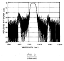
- the Bragg spectral response will be a narrow-band reflectivity peak of nearly 100% at the design wavelength, accompanied by a series of sidelobes at adjacent wavelengths.
- the calculated reflectivity spectrum of a uniform Bragg grating is shown in Figure 1 (prior art). It is important to reduce the reflectivity of the sidelobes in the Bragg response in devices where cross-talk cannot be tolerated, such as in devices for wavelength demultiplexing applications.
- Bragg gratings with reduced sidelobes in their spectral response can be achieved by recording an index modulation with a spatially varying modulation amplitude (see for example M. Matsuhara and K. O. Hill, Appl. Opt., 13, pp. 2886-2888 (1974) and I. Bennion et al., "UV-written in-fibre Bragg gratings", Tutorial review, Optical and Quantum Electronics 28, pp. 93-135 (1996)).
- the condition for an efficient sidelobe suppression is that the modulation level decreases continuously to zero at both limits of the Bragg grating.
- Appropriate apodization profiles for this task are for example Gaussian, Blackman or Hamming functions or one period of the cos 2 function (see for example D. Pastor et al., Journal of lightwave Technology, vol 14, no 11, pp. 2581-2588 (1996)).
- the first of these methods concerns the use of a beam-profile shaping filter.
- the intensity profile of the recording beams is appropriately shaped by means of absorptive, diffractive or Fabry-Perot apodizing filters, in order to generate the desired index modulation in the recording medium.
- Beam-shaping filters can be placed in the single beam incident on a uniform phase mask or in the two recording beams required for direct holographic writing in the fiber.
- two successive recording steps with different filters have to be applied, in order to generate a narrow-bandwidth spectral Bragg response without sidelobes.
- the first step produces the periodic index modulation profile
- the second step compensates variations of the average refractive index in the recording medium, which is necessary to generate a single reflected Bragg wavelength (B. Malo et al. "Apodised in-fibre Bragg grating reflectors photoimprinted using a phase mask", Electr. Lett. 2 nd Feb. 1995, Vol. 31, No. 3, pp. 223-224).
- the main drawback of the beam-shaping filter technique is that it is time consuming, difficult to use and therefore not appropriate for industrial production. It implies having to perform two exposure steps.
- the first exposure with apodized beams will induce the desired index modulation profile, but without a second exposure the local average refractive index will also vary, introducing an unwanted chirp. It is therefore necessary to expose a second time with a compensated beam to equalize the average refractive index.
- This second exposure step needs very precise alignment with respect to the first exposure.
- it is difficult to calibrate since the response of the recording medium changes after the first exposure. Therefore, the final response of the Bragg grating is difficult to control in practice.
- a second approach to write a Bragg grating having a reflection response with reduced apodized secondary maxima is the scanning beam technique.
- Variable exposure energies can be achieved by scanning focused beams or a slit mask in the recording beams with respect to the recording medium. The exposure energy is locally controlled by varying either the scanning speed or the optical power of the recording beams.
- the technique can be applied to recording with a single uniform phase mask or to direct holographic writing.
- two successive recording steps are required to generate a selective apodized Bragg grating (see J. Martin and F. Ouellette, "Novel writing technique of long and highly reflective in-fibre gratings", Electr. Lett., 30, 811-812 (1994)).
- the scanning beam technique is however a sequential recording process which is time-consuming and therefore not appropriate for the production of apodized spectral response Bragg gratings.
- the same arguments as for the beam-shaping filter technique apply and are responsible for a difficult process control.
- the improved scanning technique of the above mentioned reference from M. J. Cole et al. requires sophisticated automated positioning equipment which is able to apply a controlled dither to the fiber or the uniform phase mask, while the writing beam is scanned. For each position of the scanning beam, the movement applied to the phase mask or fiber must be carefully controlled to have a specific frequency and amplitude, in order to generate the desired variation of the local diffraction efficiency.
- a final approach to sidelobes reduction is the use of a non-holographic apodized phase mask.
- This technique has been proposed in the paper from J. Albert et al., "Apodisation of the spectral response of fibre Bragg gratings using a phase mask with variable diffraction efficiency", Electr. Lett. 2 nd Feb. 1995, Vol. 31, No. 3, pp. 222-223. It applies a single recording step with an apodized phase mask of variable diffraction efficiency.
- the apodized phase mask with variable diffraction efficiency is fabricated by direct writing in silica with a focused ion beam followed by differential wet etching.
- the first orders diffraction efficiency apodization can be performed by varying spatially the grating relief depth, the line width or both parameters at the same time.
- the apodized phase mask technique is the most appropriate technique for the production of apodized grating structures. It generates the apodized grating with a single exposure which enables high reproducibility and short fabrication times.
- the apodized phase mask structure proposed in the Albert et al. reference suffers from several severe drawbacks.
- the proposed apodized phase mask is fabricated by applying direct-write technologies which can use either a focused electron, ion or laser beam as source.
- the direct-write method has the advantage of being flexible because the grating is written one line at a time, or one writing field at a time.
- the implementation of complex apodization profiles is straight forward.
- the variable diffraction efficiency of the phase mask grating is realized by modulating the line width of the grating structure. Then, a binary surface relief is obtained in resist which can be transferred in the substrate by standard binary selective etching technology.
- Holography is a well known alternative method for fabricating phase masks.
- the sinusoidal interference pattern of two coherent optical beams is first recorded in photoresist as a surface-relief hologram which is then transferred in the substrate medium by etching.
- Holography is a parallel writing process and is therefore appropriate to the realization of large surface area phase masks.
- optical wavefronts can be generated very accurately over large surfaces by using conventional lenses or mirrors.
- the holographically recorded grating pattern is free from any positioning errors and a sub-Angstrom grating precision on the grating period over the entire grating surface is conventionally achieved. Therefore, holography is a promising. fabrication technology for apodized phase masks generating Bragg gratings with ideal, noise-free spectral responses.
- the efficiency variation of the apodized phase mask has to be realized by relief depth modulation.
- the fabrication of such grating structures in photoresist by direct holographic recording with a locally varying exposure energy has been demonstrated in A. Mitreiter et al., "Apodized diffraction grating as outcoupling element for 1.06 ⁇ m Nd:YAG laser", OSA Technical Digest Series Vol. 11, Diffractive Optics: Design, Fabrication, and Application, Rochester, 1994, pp. 282-285.
- the considered apodized grating in this reference relates to reflective output coupling elements in a laser resonator, which is a complete different application from the apodized phase mask.
- An object of the present invention is to propose a phase mask and a method for fabricating a phase mask which will satisfy the above-mentioned needs. More particularly, the present invention concerns a phase mask for modulating a collimated light beam passing therethrough as defined in claim 1; the light beam being diffracted to photoinduce by self-interference a refractive index profile in a photosensitive optical medium, the phase mask comprising:
- the grating corrugations comprise a plurality of grooves etched into the variable thin film layer.
- the substrate may comprise an etch stop layer lying under the variable thin film layer.
- the grating corrugations comprise a plurality of grooves etched into the substrate, the variable thin film layer being deposited into the grooves.
- Another object of the present invention is to propose a method for making a phase mask having a non-uniform grating profile as defined in claim 8.
- a first preferred version of the method comprises steps of:
- Another preferred version of the method for making a phase mask according to the present invention is defined in claim 17 and comprises steps of:
- this method comprises an additional step of making the uniform phase mask.
- This additional step comprises steps of:
- step b) of this method further comprises removing residual photoresist remaining on the corrugations.
- the present invention concerns a phase mask for modulating a collimated light beam passing therethrough.
- light beam is herein referring to electromagnetic radiation of any wavelength, and is not restricted to visible light. Ultra-violet light is a preferred type of radiation to be used with the present invention.
- the said light beam is devised to photoinduce a non-uniform refractive index profile in a photosensitive optical medium, more particularly to record Bragg gratings having an apodized profile in the core of optical fibers or other waveguides.
- apodized refers to a spatially varying diffraction efficiency. Both the phase mask and the produced Bragg grating have a similar apodized profile.
- the said light beam is. diffracted by the phase mask into a set of diffraction orders with spatially variable diffraction efficiencies to photoinduce a non-uniform refractive index profile in a photosensitive optical medium by self-interference, more particularly to record Bragg gratings in the core of optical fibers or other waveguides having an apodized profile.
- the phase mask (15) according to the present invention comprises a substrate (17) having an outer surface provided with a plurality of parallel grating corrugations (19).
- the grating corrugations (19) have a non-uniform relief depth across the outer surface to generate variable diffractive efficiencies, which is necessary to photoinduce a non-uniform refractive index profile in the photosensitive optical medium.
- the non-uniform relief depth is defined by a variable thin film layer (21) of variable thickness overlaying the substrate (17).
- the grating corrugations (19) of the phase mask (15) comprise a plurality of grooves (23) etched into the variable thin film layer (21).
- the substrate (17) may comprise an etch stop layer (25) lying under the variable thin film layer (21). The purpose of this etch stop layer will be further explained below.
- Figure 5 shows a second preferred embodiment of the invention, wherein the grating corrugations (19) comprise a plurality of grooves (23) etched directly into the substrate (17) itself, and wherein the variable thin film layer (21) is deposited into said grooves (23).
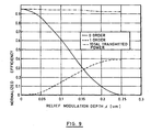
- the shape of the variable thin film layer (21) generates the desired local diffraction efficiency, and may be determined from a calibration curve based on electromagnetic grating diffraction theory such as shown in figure 9.
- the resulting refractive index profile photoinduced in the optical medium can for example have the shape of a Gaussian, Blackman or Hamming function, or one period of a squared cosine function.
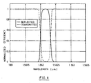
- the calculated Bragg response of an apodized fiber grating with a Gaussian modulation profile is shown in figure 6.
- the non-uniform relief depth of the grating corrugations (19) is preferably optimized in the center of the phase mask (15) for a minimization of a zero order of diffraction and a maximization of the self-interference of plus and minus first orders of diffraction of the collimated light beam, when said light beam passes through the phase mask (15) at a normal angle of incidence.
- Another variation could be to optimize the non-uniform relief depth of the grating corrugations (19) for a maximum contrast of the self-interference of a zero order and minus first order of diffraction of the collimated light beam, when said light beam passes through the phase mask (15) at an oblique angle of incidence.
- the design of a phase mask begins by analyzing the recording process of the Bragg grating in an optical fiber or waveguide. Generally, a linear relation between the exposure energy and the induced refractive index change is assumed.
- the recorded refractive index modulation from the self-inteference pattern of a phase mask can be represented by the following equation: where x denotes the axis along the apodization profile within the optical fiber or the waveguide, n o (x) represents the average index of refraction after recording and is proportional to the average recording power during exposure defined by the total transmitted light in figure 9. The total transmitted light is independent of the relief depth modulation and generates therefore a constant refractive index in the recording medium.
- ⁇ n(x) is the desired index modulation of the grating formed by the interference of the plus and minus first diffraction orders.
- the period of this grating is P, which is half of the size of the period ⁇ of the phase mask.
- ⁇ n(x) is proportional to the local first order intensity interference pattern.
- the shape of ⁇ n(x) corresponds to the desired apodization profile of the first order diffraction efficiency.
- All other parasitic grating of equal periodicity P are inclined with respect to the core of the optical fiber or waveguide. Since light guided in the core of the waveguide sees an effective refractive index averaged over the diameter of the core and the surrounding media, sufficiently inclined parasitic grating lines will be averaged out upon propagation and have therefore no influence on the reflectivity spectrum.
- a condition that only the desired grating is efficient is given in Eq. (2). d c ⁇ ⁇ n 1- 1- 4 ⁇ 2 n c 2 ⁇ 2 -1 , where ⁇ is the wavelength of the recording light in free space, d c represents the diameter of the core and n c is the refractive index of the core.
- the design of the apodized phase mask can be based on a calibration curve considering only the first order diffraction efficiency to generate the desired apodized spectral response profile.
- the total transmitted power through the phase mask has to be constant, in order to generate a uniform average refractive index which implies a single Bragg wavelength.
- Standard monomode telecommunication optical fibers satisfy Eq. (2) and therefore the design of the apodized phase mask should consider only the diffraction efficiencies of the local grating structure.
- the present invention also proposes a method for making a phase mask (15) having a non-uniform relief depth as shown in figures 4 and 5.
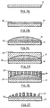
- Figure 7A to 7F illustrates the sequence of steps for making a phase mask (15) as shown in figure 4.
- the preferred version of a method according to the present invention comprises a first step a) of depositing a variable thin film layer (21) having a variable thickness on a substrate (17).
- Figure 7A shows the substrate (17).
- the materials chosen to compose the substrate (17) and the variable thin film layer (21) are preferably transparent to UV light. Potential candidates, besides others, are fused silica or quartz (SiO 2 ), magnesium fluoride (MgF 2 ), and calcium fluoride (CaF 2 ).
- the substrate (17) is preferably made of a material that can act as an etch stop for the later etching process of the variable thin film layer (21).
- an etch stop layer (25) may be deposited on the substrate (17) prior to step a).
- the material composing the etch stop layer (25) is also chosen to be transparent to UV light.
- the variable thin film layer (25) is made of SiO 2 and the substrate (17) or the etch stop layer (25) are made of MgF 2 or CaF 2 . Since high quality bulk substrates of MgF 2 or CaF 2 are expensive, it is interesting to use a fused silica substrate (17) and apply an etch stop layer (25) of MgF 2 or CaF 2 on it.
- variable thin film layer (21) having a variable thickness can be considered to generate a variable thin film layer (21) having a variable thickness.
- a straightforward approach is to structure a previously deposited uniform thin film layer. This can be achieved by polishing, diamond turning, laser ablation or any other technique.
- the preferred technique is direct deposition of the variable thickness thin film through a carefully chosen aperture or mask, as described in the Canadian Patent no 1,298,724 by Lavigne et al.
- a deposition mask having an aperture of predetermined contour is placed over the substrate (17).
- the variable thin film layer (21) is deposited through this aperture, and its thickness is varied by either rotating the deposition mask with respect to the substrate, or rotating the substrate with respect to the deposition mask.
- Another variation of this technique is to place a deposition mask having an aperture of predetermined contour over the substrate at a predetermined distance from the deposition mask. Then, the variable thin film layer (21) is deposited through the aperture of the deposition mask, the thickness of the variable thin film layer (21) being determined by the predetermined contour of the aperture and the predetermine distance of the deposition mask.
- a further variation of this technique is to chose a deposition mask having a variable deposition aperture, and vary this aperture in the deposition process to modulate the thickness of the deposited layer. More appropriate asymmetric two-dimensional profiles can be obtained, if the deposition is made through a fixed aperture at a given distance (see R.
- variable thin film layer (21) Since the variable thin film layer (21) will be etched, good adhesion to the substrate (17) is crucial and can be achieved by applying ion plating as deposition technology. It is worth noting that these deposition methods lead to very reproducible results and are suited for batch processes.
- the deposited variable thin film layer (21) can be seen in figure 7C.
- a second step of the fabrication of the phase mask shown in Figure 4 is to b) deposit a photoresist layer (27) on the variable thin film layer (21).
- the result can be seen in figure 7D.
- the photoresist layer (27) is preferably deposited by spin coating over the variable thin film layer (21). Since typical phase mask geometries for in-fiber Bragg gratings require a maximum thickness variation of approximately 250 nm and apodization profiles of several millimeters in width, the local thickness variation is negligible and does not influence the spin coating process.
- the method comprises a third step c) of recording a grating pattern (29) in the photoresist layer (27).
- This is preferably accomplished holographically by standard exposure of the photoresist (27) to a uniform interference pattern.
- exposure and development parameters are chosen to produce an optimized and uniform line width of the grating corrugations (19) over the grating surface.
- the recording of the grating pattern (29) can also be performed by direct writing with a focused electron or ion beam, or any other appropriate technique known in the art.
- the method further comprises a step d) of etching the grating pattern (29) through the photoresist layer (27) and into the variable thin film layer (21).
- the substrate or the etch-stop layer acts as an etch-stop at the phase mask borders.
- the method also comprises a step e) of removing residual photoresist (27) remaining on the variable thin film layer (17).
- FIG. 7F shows the phase mask (15) produced by the above-described method.
- a standard binary etch step generates a rectangular relief of constant line width and a well controlled relief depth modulation enabling a suppressed zero order in the phase mask center, high first order efficiency and a minimized sensitivity to the polarization state of the incident light.
- the Bragg grating response will be free of background noise and sidelobes.
- the method according to the present invention is simple to perform, and gives very good results compared to prior art methods.
- a second preferred version of the method according to the present invention is proposed to realize a non-uniform phase mask (15), as shown in figure 5.
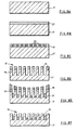
- the steps of this second method are illustrated in figure 8A to 8F. It comprises a general step of depositing a variable thin film layer (21) having a variable thickness on a uniform phase mask (31), the uniform phase mask (31) having an outer surface provided with a plurality of uniform parallel grating corrugations (19).
- uniform parallel grating it is meant that the grooves (23) have all the same depth.
- the uniform phase mask is preferably made by first depositing a photoresist layer (27) on a substrate (17), as shown in figures 8A and 8B, and then recording a grating pattern (29) in the photoresist layer (27), as shown in figure 8C.
- the grating pattern (29) is finally etched through the photoresist layer (27) and into the substrate (17), to obtain the grating corrugations (19) as shown in figure 8D.
- the above-described techniques of depositing, grating recording and etching can also be applied in this case.
- variable thin film layer (21) is deposited over the etched grating structure, as shown in figure 8E.
- the refractive index of the thin film material is preferably closely matched to the index of the substrate (17), in order to eliminate residual diffraction in the deposited regions.
- the remaining photoresist (33) and the material deposited thereon (35) are lifted off using an oxygen plasma or an alternative technique. The result is a diffraction grating of variable relief depth as schematically shown in figures 5 and 8F.
- the relief depth variation generating the desired apodization profile is obtained from a calibration curve based on electromagnetic grating theory similar to the one shown in figure 9. Compared to the previous approach, an apodized phase mask of similar optical performances can be realized. However, since in this approach the variable thin film layer (21) is not etched, improved adhesion and robustness is achieved.
- the apodized phase masks (15) fabricated with the proposed methods are easily identifiable to the naked eye.
- the relief depth modulation of the apodized phase mask (15) can also be visualized by scanning with an atomic force microscope (AFM).
- AFM atomic force microscope
- the application of a variable thin film layer (21) of variable thickness becomes visible by effectuating a slice through the phase mask structure and examining the cross section in a scanning electron microscope (SEM).
- phase mask for recording an apodized Bragg grating in an optical medium with a single exposure
- problems due to small variations of the recorded average refractive index may appear.
- These fluctuations of the average refractive index are due to either a non-uniform intensity profile of the readout beam or a variation of the total transmitted power through the phase mask (15).
- these effects can be eliminated by use of an additional intensity apodizing filter in the recodring beam.
- this intensity apodizing filter is specially designed to introduce small random intensity variations to the uniform intensity profile of the incident beam.
- a preferential embodiment of the intensity apodizer is a diffraction grating with a binary surface relief and a locally varying line-width or fill factor.
- the design and fabrication of such an element is described in M. Plante, C. Paré, P.A. Bélanger, Y. Champagne, J.M. Trudeau, M. Morin and P. Ehbets, "Laser beam variance measurements using a parabolic transmission filter", SPIE vol. 2870, pp. 22-30 (1996).
- a phase mask of rectangular surface relief grating shape with variable relief depth has been realized with high precision.
- the line width is constant over the whole grating surface and is chosen in order to enable in the center of the apodization profile a maximum contrast of the recording interference fringes.
- Electromagnetic grating theory has shown that this is achieved with a line width (or fill factor) of 0.45 of the grating period for a phase mask etched in a SiO 2 thin film or any other dielectric layer of similar index of refraction.
- Figure 9 shows the dependence of first and zero order diffraction efficiencies as a function of the relief depth.
- Phase mask parameters are chosen to realize a Bragg in-fiber grating with a Bragg wavelength in the telecommunication window around 1550 nm.
- the phase mask grating structure is etched in a variable thickness thin film layer of SiO 2 deposited over a uniform MgF 2 film, acting as an etch stop, on a fused silica substrate.
- the variable relief depth produces a smooth dependence of the first order diffraction efficiency, which is well adapted for the encoding of the desired apodization profile.
- Electromagnetic analysis has shown that the relief depth modulation is less sensitive to the polarization state of the readout laser compared to a modulation of the line width as achieved with direct writing. Therefore, apodized phase masks achieved with the new technology can be used with a broader range of illumination sources. It is further observed that the total transmitted power through the mask is practically independent of the relief depth.
- Electromagnetic analysis has also revealed that in this geometry the first order diffraction efficiency in transmission is essentially independent of the thickness of the etch stop layer.
- This thin film influences more the reflectivity and therefore, its thickness is preferably chosen to minimize reflectivity variations at the holographic recording in photoresist.
- a MgF 2 film thickness of 100 nm has been chosen, but a layer of a different material or thickness may equally be applied.
- variable thin film layer has been fabricated by deposition through an aperture, as described in the above-mentioned Canadian patent by Lavigne et al.
- a radial symmetric profile has been realized by deposition through a rotating deposition mask in close proximity to the substrate.
- This fabrication technology generates the desired tickness variation profile along a cross-section through the center of the substrate.
- the shape of the required deposition mask is shown in Figure 12. More general two-dimensional apodization profiles are more appropriate for phase mask applications.
- Such geometries can be achieved by material deposition through a fixed deposition mask at a well defined distance from the substrate, as it is described in the reference by R.
- Variable thickness thin film deposition enables a high accuracy and a high reproducibility of the desired film thickness profile. Since the fabrication technology can be applied as a batch process, it is well suited for the production of apodized phase masks.
- Standard holographic recording was applied to record a uniform grating in photoresist.
- the exposure and development parameters are adjusted to generate the optimum grating line width of 0.45.
- Selective reactive ion etching of SiO 2 is then applied to etch the photoresist grating through the variable thin film layer. This selective process shows a very low etching rate of the MgF 2 layer that acts as an etch stop, the etch depth is well controlled, thus resulting in optimum phase mask performance.
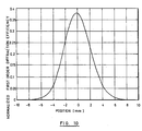
- first order diffraction efficiencies of fabricated prototype phase masks are shown in Figure 13. It is observed that the prototype phase mask generates the desired Gaussian first order apodization profile. A FWHM of 5.3 mm has been measured, which is close to the design value. A small increase of the FWHM is explained by the efficiency measurement with an optical spot of 2.0 mm diameter. Maximum first order efficiencies in the center is 37% and the zero order was suppressed below 3%. The given efficiency values are measured with respect to the incident beam power on the grating. They contain any reflection or absorption losses. Compared to previously achieved results with direct writing, a much higher modulation range of the first-order diffraction efficiency is demonstrated.
- the prototype masks have resisted to pulses of energy levels up to 13 J/cm 2 without deterioration.
- Adhesion of the etched grating structure has been verified and complies with military specification MIL-C-48497A paragraph 3.4.1.1.
Landscapes
- Physics & Mathematics (AREA)
- General Physics & Mathematics (AREA)
- Optics & Photonics (AREA)
- Engineering & Computer Science (AREA)
- Manufacturing & Machinery (AREA)
- Diffracting Gratings Or Hologram Optical Elements (AREA)
- Analysing Materials By The Use Of Radiation (AREA)
Claims (19)
- Un masque de phase (15) pour moduler un faisceau lumineux collimaté le traversant, le faisceau lumineux étant diffracté pour photoinduire par auto-interférence un profile d'indice de réfraction dans un milieu optique photosensible, le masque de phase comprenant:un substrat (17) ayant une surface externe munie d'une pluralité d'ondulations parallèles de réseau (19), les ondulations de réseau (19) ayant une profondeur de relief non-uniforme le long de la surface externe, la profondeur de relief non-uniforme étant définie par une couche mince variable (21) ayant une épaisseur variable recouvrant le substrat (17), le masque de phase (15) étant caractérisé en ce que la profondeur de relief non-uniforme est maximale à un centre des ondulations de réseau et diminue continuellement vers zéro à des extrémités opposées desdites ondulations de réseau pour photoinduire un profile d'indice de réfraction apodisé dans le milieu optique photosensible.
- Un masque de phase (15) selon la revendication 1, caractérisé en ce que les ondulations de réseau (19) comprennent une pluralité de rainures (23) gravées dans la couche mince variable (21).
- Un masque de phase (15) selon la revendication 2, caractérisé en ce que le substrat (17) comprend une couche d'arrêt de gravure (25) étendue sous la couche mince variable (21).
- Un masque de phase (15) selon la revendication 1, caractérisé en ce que les ondulations de réseau (19) comprennent une pluralité de rainures (23) gravées dans le substrat (17) et où la couche mince variable (21) est déposée dans lesdites rainures (23).
- Un masque de phase (15) selon la revendication 1, caractérisé en ce que la profondeur de relief non-uniforme a une forme choisie de façon à photoinduire un profile d'indice de réfraction dans le milieu optique photosensible qui a une forme définie par une fonction choisie du groupe comprenant les fonctions Gaussienne, Blackman et Hamming et une période d'une fonction sinus ou cosinus au carré.
- Un masque de phase (15) selon la revendication 1, caractérisé en ce que la profondeur de relief non-uniforme des ondulations de réseau est optimisée pour une minimalisation d'un ordre de diffraction zéro et un contraste maximum d'auto-interférence des premiers ordres de diffraction positif et négatif du faisceau lumineux collimaté dans un centre des ondulations de réseau (19) lorsque ledit faisceau lumineux traverse le masque de phase à un angle d'incidence normal.
- Un masque de phase (15) selon la revendication 1, caractérisé en ce que la profondeur de relief non-uniforme des ondulations de réseau est optimisé pour un contraste maximum de l'auto-interférence d'un ordre de diffraction zéro et d'un premier ordre de diffraction négatif du faisceau lumineux collimaté lorsque ledit faisceau lumineux traverse le masque de phase à un angle d'incidence oblique.
- Une méthode pour fabriquer un masque de phase (15) pour moduler un faisceau lumineux collimaté traversant celui-ci, le faisceau lumineux étant diffracté pour photoinduire par auto-interférence un profile d'index de réfraction dans un milieu photosensible, ledit masque de phase ayant un profile de réseau non uniforme, la méthode étant caractérisée en ce qu'elle est pour fabriquer un masque de phase pour photoinduire un profile d'indice de réfraction apodisé dans le milieu photosensible, la méthode étant de plus caractérisée en ce qu'elle comprend les étapes de:a) déposer une couche mince variable (21) ayant une épaisseur variable sur un substrat (17), ladite épaisseur variable étant maximum à un centre de la couche mince variable (21) et diminuant continuellement vers zéro à des extrémités opposées de celle-ci;b) déposer une couche de résine photosensible (27) sur la couche mince variable (21);c) enregistrer un patron de réseau (29) dans la couche de résine photosensible (27);d) graver le patron de réseau (29) à travers la couche de résine photosensible (27) et dans la couche mince variable (21), l'épaisseur variable de la couche mince variable (21) créant le profile de réseau non-uniforme; ete) retirer de la résine photosensible résiduelle (27) restant sur la couche mince variable (21).
- Une méthode pour fabriquer un masque de phase (15) selon la revendication 8, caractérisée en ce que le substrat (17) comprend une couche d'arrêt de gravure déposée sur celle-ci avant l'étape a).
- Une méthode pour fabriquer un masque de phase (15) selon la revendication 8, caractérisée en ce que l'étape a) de déposer une couche mince variable (21) comprend les étapes de:i) placer un masque de déposition ayant une ouverture de contour prédéterminé au-dessus du substrat; etii) déposer la couche mince variable (21) à travers ladite ouverture, l'épaisseur de la couche mince variable (21) étant variée en déplaçant le masque de déposition par rapport au substrat.
- Une méthode pour fabriquer un masque de phase (15) selon la revendication 8, étant caractérisée en ce que l'étapea) de déposer une couche mince variable (21) comprend les étapes de:i) placer un masque de déposition ayant une ouverture de contour prédéterminé au-dessus du substrat; etii) déposer la couche mince variable (21) à travers ladite ouverture, l'épaisseur de la couche mince variable (21) étant variée en déplaçant le substrat (17) par rapport au masque de déposition.
- Une méthode pour fabriquer un masque de phase (15) selon la revendication 8, caractérisée en ce que l'étape a) de déposer une couche mince variable (21) comprend les étapes de:i) placer un masque de déposition ayant une ouverture de contour variable au-dessus du substrat (17); etii) déposer la couche mince variable (21) à travers ladite ouverture, l'épaisseur de la couche mince variable (21) étant variée en variant ladite ouverture.
- Une méthode pour fabriquer un masque de phase (15) selon la revendication 8, caractérisée en ce que l'étape a) de déposer une couche mince variable (21) comprend les étapes de:i) placer un masque de déposition ayant une ouverture de contour prédéterminé au-dessus du substrat à une distance prédéterminée dudit substrat; etii) déposer la couche mince variable (21) à travers ladite ouverture, le masque de déposition étant gardé fixé au-dessus du substrat, l'épaisseur de la couche mince variable (21) étant déterminé par le contour prédéterminé de ladite ouverture et la distance prédéterminée dudit masque de déposition par rapport au substrat (17).
- Une méthode pour fabriquer un masque de phase (15) selon la revendication 8, caractérisée en ce que l'étape a) de déposer une couche mince variable (21) comprend les étapes de:i) déposer une couche mince primaire, etii) structurer la couche mince primaire pour obtenir l'épaisseur variable de la couche mince.
- Une méthode pour fabriquer un masque de phase (15) selon la revendication 14, caractérisée en ce que dans l'étape a) ii) la structuration de la couche mince primaire est obtenue par un procédé choisi du groupe comprenant le polissage, l'ablation au laser et le tour au diamant.
- Une méthode pour fabriquer un masque de phase (15) selon la revendication 8, caractérisée en ce que dans l'étape c) le patron de réseau est enregistré par un procédé choisi du groupe comprenant l'écriture holographique, l'écriture directe avec un faisceau de particule focalisé, et l'écriture directe avec un faisceau optique focalisé.
- Une méthode pour fabriquer un masque de phase (15) pour moduler un faisceau lumineux collimaté traversant ce dernier, le faisceau lumineux étant diffracté pour photoinduire par auto-interférence un profile d'index de réfraction dans un milieu photosensible, ledit masque de phase ayant un profile de réseau non-uniforme, la méthode étant caractérisée en ce qu'elle est pour fabriquer un masque de phase pour photoinduire un profile d'indice de réfraction apodisé dans le milieu photosensible, la méthode étant également caractérisée en ce qu'elle comprend les étapes de:a) déposer une couche mince variable ayant une épaisseur variable (21) sur un masque de phase uniforme (31), ladite épaisseur variable étant minimum en un centre de la couche mince variable (21) et augmentant continuellement vers un maximum à des extrémités opposées de celles-ci, le masque de phase uniforme (31) ayant une surface externe munie d'une pluralité d'ondulations de réseaux (19) parallèles de profondeur uniforme, les ondulations définissant des rainures et des crêtes de façon à ce qu'une portion de la couche mince est déposée sur les crêtes et une autre portion de la couche mince est déposée dans les rainures, etb) retirer la portion de la couche mince variable (21) qui est déposée sur les crêtes des ondulations (19).
- Une méthode pour fabriquer un masque de phase (15) selon la revendication 17, étant caractérisée en ce qu'elle comprend avant l'étape a) une étape de fabriquer le masque de phase uniforme (31), ladite étape comprenant les étapes de:la méthode étant également caractérisée en ce que l'étape b) comprend retirer de la résine photosensible résiduelle (33) restant sur les ondulations de réseau (19).i) déposer une couche de résine photosensible (27) sur un substrat (17);ii) enregistrer un patron de réseau (29) dans la couche de résine photosensible (27); etiii) graver le patron de réseau (29) à travers la couche de résine photosensible (27) et dans le substrat (17) pour obtenir lesdites ondulations de réseau (19),
- Une méthode pour fabriquer un masque de phase (15) selon la revendication 18, caractérisée en ce que dans ii) le patron de réseau (29) est enregistré par un procédé choisi du groupe comprenant l'écriture holographique, l'écriture directe avec un faisceau de particule focalisé, et l'écriture directe avec un faisceau optique focalisé.
Applications Claiming Priority (3)
| Application Number | Priority Date | Filing Date | Title |
|---|---|---|---|
| CA2197706 | 1997-02-14 | ||
| CA002197706A CA2197706A1 (fr) | 1997-02-14 | 1997-02-14 | Methode de fabrication de masque de phase apodise |
| PCT/CA1998/000112 WO1998036297A1 (fr) | 1997-02-14 | 1998-02-11 | Sources de curietherapie de faible energie encapsulees |
Publications (2)
| Publication Number | Publication Date |
|---|---|
| EP0960347A1 EP0960347A1 (fr) | 1999-12-01 |
| EP0960347B1 true EP0960347B1 (fr) | 2002-07-03 |
Family
ID=4159949
Family Applications (1)
| Application Number | Title | Priority Date | Filing Date |
|---|---|---|---|
| EP98902911A Expired - Lifetime EP0960347B1 (fr) | 1997-02-14 | 1998-02-11 | Masque de phase presentant une efficacite de diffraction variable dans l'espace |
Country Status (7)
| Country | Link |
|---|---|
| US (1) | US6545808B1 (fr) |
| EP (1) | EP0960347B1 (fr) |
| JP (1) | JP2001511906A (fr) |
| AU (1) | AU731744B2 (fr) |
| CA (1) | CA2197706A1 (fr) |
| DE (1) | DE69806343D1 (fr) |
| WO (1) | WO1998036297A1 (fr) |
Cited By (2)
| Publication number | Priority date | Publication date | Assignee | Title |
|---|---|---|---|---|
| EP3785054A1 (fr) * | 2018-04-23 | 2021-03-03 | Facebook Technologies, LLC | Réseaux à profondeurs variables formés à l'aide d'une planarisation pour dispositifs d'affichage à guide d'ondes |
| TWI803172B (zh) * | 2019-11-12 | 2023-05-21 | 美商應用材料股份有限公司 | 形成衍射光學元件的方法 |
Families Citing this family (93)
| Publication number | Priority date | Publication date | Assignee | Title |
|---|---|---|---|---|
| US20030107787A1 (en) * | 2001-09-26 | 2003-06-12 | Arkady Bablumyan | Planar and fiber optical apodized diffraction structures fabrication |
| US20030107786A1 (en) * | 2001-09-26 | 2003-06-12 | Arkady Bablumyan | Precision optical apparatus utilizing non-optically smooth material |
| JP4632103B2 (ja) * | 2001-10-01 | 2011-02-16 | セイコーエプソン株式会社 | フォトマスク |
| JP4556143B2 (ja) * | 2001-10-01 | 2010-10-06 | セイコーエプソン株式会社 | 位相格子マスクの製造方法及びフォトマスクの製造方法 |
| US7050155B2 (en) | 2001-10-30 | 2006-05-23 | Pixelligent Technologies Llc | Advanced exposure techniques for programmable lithography |
| US6654521B2 (en) * | 2002-01-23 | 2003-11-25 | Teraxion Inc. | Diffraction compensation of FBG phase masks for multi-channel sampling applications |
| WO2006072071A2 (fr) * | 2004-12-30 | 2006-07-06 | Phoseon Technology Inc. | Procedes et systemes concernant des sources lumineuses destinees a etre utilisees dans des procedes industriels |
| EP2009676B8 (fr) | 2002-05-08 | 2012-11-21 | Phoseon Technology, Inc. | Systèmes d'inspection de matériaux à semi-conducteur |
| US6830702B2 (en) * | 2002-06-07 | 2004-12-14 | Taiwan Semiconductor Manufacturing Co. Ltd | Single trench alternating phase shift mask fabrication |
| US7310463B2 (en) * | 2002-09-09 | 2007-12-18 | Kyocera Corporation | Optical structural body, its manufacturing method and optical element |
| US7239594B2 (en) * | 2003-02-07 | 2007-07-03 | Imation Corp. | Self-referenced holography using element formed on a holographic medium |
| KR100908234B1 (ko) * | 2003-02-13 | 2009-07-20 | 삼성모바일디스플레이주식회사 | 전계 발광 표시 장치 및 이의 제조방법 |
| EP1482494A3 (fr) * | 2003-05-28 | 2007-08-29 | Matsushita Electric Industrial Co., Ltd. | Procédé de fabrication d'un disque maître pour supports d'enregistrement optique d'informations |
| US20040244425A1 (en) * | 2003-06-09 | 2004-12-09 | Xiaolin Tong | Fabrication of photosensitive couplers |
| CN100359299C (zh) * | 2003-11-03 | 2008-01-02 | 中国科学院长春光学精密机械与物理研究所 | 一种光路对称分布的光栅衍射效率测试仪 |
| US7277604B2 (en) * | 2003-12-12 | 2007-10-02 | Lxsix Photonics Inc. | Method and apparatus for inducing an index of refraction change on a substrate sensitive to electromagnetic radiation |
| TWI312583B (en) * | 2004-03-18 | 2009-07-21 | Phoseon Technology Inc | Micro-reflectors on a substrate for high-density led array |
| WO2005101067A1 (fr) * | 2004-04-13 | 2005-10-27 | Matsushita Electric Industrial Co., Ltd. | Élément de condensation et dispositif de formation d'images à semiconducteur |
| US7289699B1 (en) * | 2004-04-29 | 2007-10-30 | Northrop Grumman Corporation | Grating apodization technique for diffused optical waveguides |
| US7280206B2 (en) * | 2004-09-13 | 2007-10-09 | Agilent Technologies, Inc. | Method and apparatus to improve the dynamic range of optical devices using spatial apodization |
| US7427466B2 (en) * | 2004-11-29 | 2008-09-23 | Imation Corp. | Anti-reflection optical data storage disk master |
| US20060204185A1 (en) * | 2005-03-09 | 2006-09-14 | Konica Minolta Holdings, Inc. | Diffractive optical element and bidirectional optical communication module using the same |
| CN1322341C (zh) * | 2005-06-08 | 2007-06-20 | 中国科学院上海光学精密机械研究所 | 632.8纳米波长的高衍射效率石英透射光栅 |
| CN1322339C (zh) * | 2005-06-08 | 2007-06-20 | 中国科学院上海光学精密机械研究所 | 532纳米波长的高衍射效率石英透射光栅 |
| CN1322340C (zh) * | 2005-06-08 | 2007-06-20 | 中国科学院上海光学精密机械研究所 | 1053纳米波长的高衍射效率石英透射光栅 |
| DE102005044730B4 (de) * | 2005-09-19 | 2008-12-11 | Swet Optics Gmbh | Optisches Element und Verfahren zur Steuerung seiner Übertragungsfunktion |
| CN100340875C (zh) * | 2006-03-08 | 2007-10-03 | 中国科学院上海光学精密机械研究所 | 800纳米波段的石英透射偏振分束光栅 |
| CN100340876C (zh) * | 2006-03-22 | 2007-10-03 | 中国科学院上海光学精密机械研究所 | 532纳米波长的高密度深刻蚀石英透射偏振分束光栅 |
| CN100340877C (zh) * | 2006-03-22 | 2007-10-03 | 中国科学院上海光学精密机械研究所 | 632.8纳米波长背入射式石英反射偏振分束光栅 |
| WO2008044686A1 (fr) * | 2006-10-10 | 2008-04-17 | Asahi Glass Co., Ltd. | Élément de diffraction et dispositif à tête optique équipé de celui-ci |
| US7773307B2 (en) * | 2006-12-12 | 2010-08-10 | Northrop Grumman Space & Mission Systems Corporation | Phase mask with continuous azimuthal variation for a coronagraph imaging system |
| US20110038049A1 (en) * | 2007-02-23 | 2011-02-17 | Nanocomp Ltd | Method for designing a diffraction grating structure and a diffraction grating structure |
| WO2010138554A1 (fr) * | 2009-05-27 | 2010-12-02 | Redfern Integrated Optics, Inc. | Fabrication de dispositif avec réseaux de bragg plans supprimant des effets parasites |
| US8532450B1 (en) * | 2009-12-23 | 2013-09-10 | Western Digital (Fremont), Llc | Optical grating and method of manufacture |
| CN103620356B (zh) * | 2011-04-20 | 2016-04-13 | 惠普发展公司,有限责任合伙企业 | 光探测系统 |
| WO2012144997A1 (fr) | 2011-04-20 | 2012-10-26 | Hewlett-Packard Development Company, L.P. | Éléments optiques basés sur un réseau de diffraction sous-longueur d'onde |
| WO2016020630A2 (fr) | 2014-08-08 | 2016-02-11 | Milan Momcilo Popovich | Illuminateur laser en guide d'ondes comprenant un dispositif de déchatoiement |
| EP2842003B1 (fr) | 2012-04-25 | 2019-02-27 | Rockwell Collins, Inc. | Affichage grand angle holographique |
| DE102012108170B4 (de) * | 2012-09-03 | 2015-01-22 | Bundesdruckerei Gmbh | Sicherheitselement und Verfahren zur Herstellung eines Sicherheitselements |
| US9933684B2 (en) | 2012-11-16 | 2018-04-03 | Rockwell Collins, Inc. | Transparent waveguide display providing upper and lower fields of view having a specific light output aperture configuration |
| US9354401B2 (en) | 2013-01-30 | 2016-05-31 | Hewlett Packard Enterprise Development Lp | Optical connector having a cleaning element |
| US9240255B2 (en) * | 2013-03-06 | 2016-01-19 | University Of Oregon | Device and method for creating Gaussian aberration-corrected electron beams |
| CN103197366B (zh) * | 2013-03-13 | 2015-06-17 | 北京工业大学 | 基于异质结光栅的偏振滤波器及制备方法 |
| UA123038C2 (uk) * | 2014-05-22 | 2021-02-10 | Аустреліан Нуклеар Саєнс Енд Текнолоджі Органісейшн | Візуалізація гамма-випромінювання |
| US9632226B2 (en) | 2015-02-12 | 2017-04-25 | Digilens Inc. | Waveguide grating device |
| WO2016146963A1 (fr) * | 2015-03-16 | 2016-09-22 | Popovich, Milan, Momcilo | Dispositif de guide d'onde incorporant un conduit de lumière |
| US9618664B2 (en) | 2015-04-15 | 2017-04-11 | Finisar Corporation | Partially etched phase-transforming optical element |
| WO2017060665A1 (fr) | 2015-10-05 | 2017-04-13 | Milan Momcilo Popovich | Afficheur à guide d'ondes |
| JP6882316B2 (ja) * | 2016-03-04 | 2021-06-02 | アプライド マテリアルズ インコーポレイテッドApplied Materials,Incorporated | ワイヤグリッド偏光板製造方法 |
| US10539723B2 (en) | 2016-10-19 | 2020-01-21 | Finisar Corporation | Phase-transforming optical reflector formed by partial etching or by partial etching with reflow |
| EP3548939A4 (fr) | 2016-12-02 | 2020-11-25 | DigiLens Inc. | Dispositif de guide d'ondes à éclairage de sortie uniforme |
| US10545346B2 (en) | 2017-01-05 | 2020-01-28 | Digilens Inc. | Wearable heads up displays |
| KR101919067B1 (ko) | 2017-04-27 | 2018-11-19 | 세종공업 주식회사 | 저수차 렌즈 제조방법 |
| FI128376B (en) * | 2017-06-02 | 2020-04-15 | Dispelix Oy | Process for the preparation of a diffractive grating with varying efficiency and a diffraction grating |
| FI128574B (en) * | 2017-06-02 | 2020-08-14 | Dispelix Oy | Height-modulated diffractive master plate and process for its manufacture |
| WO2019027931A1 (fr) * | 2017-07-31 | 2019-02-07 | Rutgers, The State University Of New Jersey | Appareil et procédé de modulation spatiale de lumière sur la base d'un démouillage pour lasers à haute puissance |
| CN114721242B (zh) | 2018-01-08 | 2025-08-15 | 迪吉伦斯公司 | 用于制造光学波导的方法 |
| JP7456929B2 (ja) | 2018-01-08 | 2024-03-27 | ディジレンズ インコーポレイテッド | 導波管セルを製造するためのシステムおよび方法 |
| JP7404243B2 (ja) | 2018-01-08 | 2023-12-25 | ディジレンズ インコーポレイテッド | 導波管セル内のホログラフィック格子の高スループット記録のためのシステムおよび方法 |
| CN108110600B (zh) * | 2018-02-05 | 2023-08-15 | 长春新产业光电技术有限公司 | 一种多光束相位扰动装置及方法 |
| US10818499B2 (en) | 2018-02-21 | 2020-10-27 | Varian Semiconductor Equipment Associates, Inc. | Optical component having variable depth gratings and method of formation |
| US11067726B2 (en) * | 2018-04-23 | 2021-07-20 | Facebook Technologies, Llc | Gratings with variable depths for waveguide displays |
| US10649141B1 (en) * | 2018-04-23 | 2020-05-12 | Facebook Technologies, Llc | Gratings with variable etch heights for waveguide displays |
| CN112513688B (zh) | 2018-07-19 | 2023-05-26 | 应用材料公司 | 可变高度的斜向光栅方法 |
| US11675114B2 (en) * | 2018-07-23 | 2023-06-13 | Ii-Vi Delaware, Inc. | Monolithic structured light projector |
| US10935799B2 (en) * | 2018-10-23 | 2021-03-02 | Applied Materials, Inc. | Optical component having depth modulated angled gratings and method of formation |
| TWI864336B (zh) * | 2018-11-07 | 2024-12-01 | 美商應用材料股份有限公司 | 使用灰調微影術及傾斜蝕刻的深度調節傾斜光柵 |
| US10690821B1 (en) * | 2018-12-14 | 2020-06-23 | Applied Materials, Inc. | Methods of producing slanted gratings |
| JPWO2020145218A1 (ja) | 2019-01-10 | 2021-11-04 | 富士フイルム株式会社 | 構造体、固体撮像素子および画像表示装置 |
| WO2020149956A1 (fr) | 2019-01-14 | 2020-07-23 | Digilens Inc. | Affichage de guide d'ondes holographique avec couche de commande de lumière |
| US11150394B2 (en) * | 2019-01-31 | 2021-10-19 | Facebook Technologies, Llc | Duty cycle range increase for waveguide combiners |
| US20200247017A1 (en) | 2019-02-05 | 2020-08-06 | Digilens Inc. | Methods for Compensating for Optical Surface Nonuniformity |
| US20220283377A1 (en) | 2019-02-15 | 2022-09-08 | Digilens Inc. | Wide Angle Waveguide Display |
| EP3924759B1 (fr) | 2019-02-15 | 2025-07-30 | Digilens Inc. | Procédés et appareils pour fournir un affichage de guide d'ondes holographique à l'aide de réseaux intégrés |
| US10976483B2 (en) * | 2019-02-26 | 2021-04-13 | Facebook Technologies, Llc | Variable-etch-depth gratings |
| US10809448B1 (en) * | 2019-04-18 | 2020-10-20 | Facebook Technologies, Llc | Reducing demolding stress at edges of gratings in nanoimprint lithography |
| EP3980825A4 (fr) | 2019-06-07 | 2023-05-03 | Digilens Inc. | Guides d'ondes incorporant des réseaux transparents et réfléchissants et procédés de fabrication associés |
| WO2020264056A1 (fr) * | 2019-06-24 | 2020-12-30 | Nlight, Inc. | Distribution d'intensité homogénéisée de manière fonctionnelle pour la fabrication additive ou d'autres applications de traitement au laser industriel |
| JP2022546413A (ja) | 2019-08-29 | 2022-11-04 | ディジレンズ インコーポレイテッド | 真空回折格子および製造方法 |
| CN110543029B (zh) * | 2019-09-06 | 2023-05-02 | Ii-Vi特拉华有限公司 | 单片结构光投影仪 |
| WO2021063910A1 (fr) * | 2019-09-30 | 2021-04-08 | Carl Zeiss Jena Gmbh | Structures de réseau dissimulées |
| US11662524B2 (en) | 2020-03-13 | 2023-05-30 | Applied Materials, Inc. | Forming variable depth structures with laser ablation |
| KR20230016014A (ko) * | 2020-06-03 | 2023-01-31 | 어플라이드 머티어리얼스, 인코포레이티드 | 도파관 격자들의 구배 캡슐화 |
| FI131825B1 (en) * | 2020-06-17 | 2025-12-18 | Dispelix Oy | Method for producing an optical element, an optical element, and apparatus for producing an optical element |
| US20220082739A1 (en) * | 2020-09-17 | 2022-03-17 | Facebook Technologies, Llc | Techniques for manufacturing variable etch depth gratings using gray-tone lithography |
| US11709422B2 (en) | 2020-09-17 | 2023-07-25 | Meta Platforms Technologies, Llc | Gray-tone lithography for precise control of grating etch depth |
| WO2022150841A1 (fr) * | 2021-01-07 | 2022-07-14 | Digilens Inc. | Structures de réseau pour guides d'ondes de couleur |
| CN116982225A (zh) * | 2021-03-05 | 2023-10-31 | Ipg光子公司 | 腔内全息激光模式转换器 |
| JP2023109013A (ja) * | 2022-01-26 | 2023-08-07 | パナソニックIpマネジメント株式会社 | 微細構造の製造方法 |
| CN114594612B (zh) * | 2022-03-04 | 2024-04-26 | 南京邮电大学 | 基于变迹光栅组的捕获原子、操纵和读取原子态的方法 |
| CN120112820A (zh) * | 2022-10-27 | 2025-06-06 | 应用材料公司 | 用于调变光栅绕射效率的喷墨式梯度折射率材料 |
| CN119433436B (zh) * | 2025-01-10 | 2025-09-19 | 上海大学 | 掩膜板结构、光学结构的形成方法、衍射光波导 |
| CN119506795B (zh) * | 2025-01-21 | 2025-08-26 | 上海大学 | 沉积辅助结构、光学结构的形成方法及衍射光波导 |
Citations (2)
| Publication number | Priority date | Publication date | Assignee | Title |
|---|---|---|---|---|
| US4936665A (en) * | 1987-10-25 | 1990-06-26 | Whitney Theodore R | High resolution imagery systems and methods |
| US5587815A (en) * | 1992-09-17 | 1996-12-24 | Minolta Camera Kabushiki Kaisha | Phase modulation holographic device for generating two different wavefronts |
Family Cites Families (6)
| Publication number | Priority date | Publication date | Assignee | Title |
|---|---|---|---|---|
| US5367588A (en) * | 1992-10-29 | 1994-11-22 | Her Majesty The Queen In Right Of Canada, As Represented By The Minister Of Communications | Method of fabricating Bragg gratings using a silica glass phase grating mask and mask used by same |
| JP2690430B2 (ja) | 1992-07-06 | 1997-12-10 | ワイケイケイ株式会社 | スライドファスナー用務歯の成形方法及び装置 |
| US5413884A (en) * | 1992-12-14 | 1995-05-09 | American Telephone And Telegraph Company | Grating fabrication using electron beam lithography |
| US5327515A (en) | 1993-01-14 | 1994-07-05 | At&T Laboratories | Method for forming a Bragg grating in an optical medium |
| JPH07311307A (ja) * | 1993-07-02 | 1995-11-28 | Xerox Corp | 2進回折光学要素における位相アポダイゼーション |
| US6313473B1 (en) * | 1999-05-14 | 2001-11-06 | :Uconn Technology Inc. | Device for producing apodized gratings |
-
1997
- 1997-02-14 CA CA002197706A patent/CA2197706A1/fr not_active Abandoned
-
1998
- 1998-02-11 JP JP53519098A patent/JP2001511906A/ja active Pending
- 1998-02-11 US US09/403,678 patent/US6545808B1/en not_active Expired - Fee Related
- 1998-02-11 EP EP98902911A patent/EP0960347B1/fr not_active Expired - Lifetime
- 1998-02-11 DE DE69806343T patent/DE69806343D1/de not_active Expired - Lifetime
- 1998-02-11 AU AU59789/98A patent/AU731744B2/en not_active Ceased
- 1998-02-11 WO PCT/CA1998/000112 patent/WO1998036297A1/fr not_active Ceased
Patent Citations (2)
| Publication number | Priority date | Publication date | Assignee | Title |
|---|---|---|---|---|
| US4936665A (en) * | 1987-10-25 | 1990-06-26 | Whitney Theodore R | High resolution imagery systems and methods |
| US5587815A (en) * | 1992-09-17 | 1996-12-24 | Minolta Camera Kabushiki Kaisha | Phase modulation holographic device for generating two different wavefronts |
Cited By (2)
| Publication number | Priority date | Publication date | Assignee | Title |
|---|---|---|---|---|
| EP3785054A1 (fr) * | 2018-04-23 | 2021-03-03 | Facebook Technologies, LLC | Réseaux à profondeurs variables formés à l'aide d'une planarisation pour dispositifs d'affichage à guide d'ondes |
| TWI803172B (zh) * | 2019-11-12 | 2023-05-21 | 美商應用材料股份有限公司 | 形成衍射光學元件的方法 |
Also Published As
| Publication number | Publication date |
|---|---|
| JP2001511906A (ja) | 2001-08-14 |
| CA2197706A1 (fr) | 1998-08-14 |
| AU5978998A (en) | 1998-09-08 |
| WO1998036297A1 (fr) | 1998-08-20 |
| AU731744B2 (en) | 2001-04-05 |
| US6545808B1 (en) | 2003-04-08 |
| EP0960347A1 (fr) | 1999-12-01 |
| DE69806343D1 (de) | 2002-08-08 |
Similar Documents
| Publication | Publication Date | Title |
|---|---|---|
| EP0960347B1 (fr) | Masque de phase presentant une efficacite de diffraction variable dans l'espace | |
| EP0606726B1 (fr) | Méthode de fabrication d'un réseau de Bragg dans un milieu optique | |
| JP3330858B2 (ja) | 連続的にチャープした位相マスクの製造方法 | |
| US6823115B2 (en) | Optical structures distributed among multiple optical waveguides | |
| US5760960A (en) | Cascaded self-induced holography | |
| KR100302122B1 (ko) | 광도파관과광도파관의광경로에브래그격자를제조하는방법및장치 | |
| EP1025457B1 (fr) | Fabrication de reseaux pour guides d'ondes optiques | |
| FR2697642A1 (fr) | Méthode de fabrication de réseaux de diffraction de Bragg. | |
| US20030107787A1 (en) | Planar and fiber optical apodized diffraction structures fabrication | |
| JPH1054914A (ja) | 光導波路に格子を形成する方法 | |
| US5956442A (en) | Bragg reflection gratings in optical fibres | |
| KR100334799B1 (ko) | 광섬유격자 제작 장치 및 방법 | |
| US5953471A (en) | Optical communication system having short period reflective Bragg gratings | |
| US6483965B1 (en) | Method of writing a bragg diffraction grating | |
| CA2281787C (fr) | Masque de phase presentant une efficacite de diffraction variable dans l'espace | |
| JP3693494B2 (ja) | チャープ型光ファイバフィルタの製造方法及びチャープ型光ファイバフィルタ | |
| GB2289770A (en) | Writing bragg gratings in photosensitive waveguides | |
| US6778733B2 (en) | Lithographic fabrication of phase mask for fiber Bragg gratings | |
| US20030107786A1 (en) | Precision optical apparatus utilizing non-optically smooth material | |
| JPH11295541A (ja) | 導波路型回折格子の製造方法及び導波路型回折格子製造装置 | |
| EP1078288B1 (fr) | Procede d'inscription de reseaux de bragg | |
| JP4543128B2 (ja) | 光導波路ブラッググレーティングの製造方法および製造装置 | |
| Ehbets et al. | Fabrication method for phase mask with spatially variable diffraction efficiency | |
| Greiner et al. | Planar lithographic holography as enabler of integrated photonics |
Legal Events
| Date | Code | Title | Description |
|---|---|---|---|
| PUAI | Public reference made under article 153(3) epc to a published international application that has entered the european phase |
Free format text: ORIGINAL CODE: 0009012 |
|
| 17P | Request for examination filed |
Effective date: 19990914 |
|
| AK | Designated contracting states |
Kind code of ref document: A1 Designated state(s): DE DK FR GB IT SE |
|
| 17Q | First examination report despatched |
Effective date: 20000704 |
|
| GRAG | Despatch of communication of intention to grant |
Free format text: ORIGINAL CODE: EPIDOS AGRA |
|
| RAP1 | Party data changed (applicant data changed or rights of an application transferred) |
Owner name: STOCKERYALE CANADA INC. Owner name: INSTITUT NATIONAL D'OPTIQUE |
|
| GRAG | Despatch of communication of intention to grant |
Free format text: ORIGINAL CODE: EPIDOS AGRA |
|
| GRAH | Despatch of communication of intention to grant a patent |
Free format text: ORIGINAL CODE: EPIDOS IGRA |
|
| GRAH | Despatch of communication of intention to grant a patent |
Free format text: ORIGINAL CODE: EPIDOS IGRA |
|
| GRAA | (expected) grant |
Free format text: ORIGINAL CODE: 0009210 |
|
| AK | Designated contracting states |
Kind code of ref document: B1 Designated state(s): DE DK FR GB IT SE |
|
| PG25 | Lapsed in a contracting state [announced via postgrant information from national office to epo] |
Ref country code: IT Free format text: LAPSE BECAUSE OF FAILURE TO SUBMIT A TRANSLATION OF THE DESCRIPTION OR TO PAY THE FEE WITHIN THE PRESCRIBED TIME-LIMIT;WARNING: LAPSES OF ITALIAN PATENTS WITH EFFECTIVE DATE BEFORE 2007 MAY HAVE OCCURRED AT ANY TIME BEFORE 2007. THE CORRECT EFFECTIVE DATE MAY BE DIFFERENT FROM THE ONE RECORDED. Effective date: 20020703 Ref country code: FR Free format text: LAPSE BECAUSE OF NON-PAYMENT OF DUE FEES Effective date: 20020703 |
|
| REF | Corresponds to: |
Ref document number: 69806343 Country of ref document: DE Date of ref document: 20020808 |
|
| PG25 | Lapsed in a contracting state [announced via postgrant information from national office to epo] |
Ref country code: SE Free format text: LAPSE BECAUSE OF FAILURE TO SUBMIT A TRANSLATION OF THE DESCRIPTION OR TO PAY THE FEE WITHIN THE PRESCRIBED TIME-LIMIT Effective date: 20021003 Ref country code: DK Free format text: LAPSE BECAUSE OF FAILURE TO SUBMIT A TRANSLATION OF THE DESCRIPTION OR TO PAY THE FEE WITHIN THE PRESCRIBED TIME-LIMIT Effective date: 20021003 |
|
| PG25 | Lapsed in a contracting state [announced via postgrant information from national office to epo] |
Ref country code: DE Free format text: LAPSE BECAUSE OF FAILURE TO SUBMIT A TRANSLATION OF THE DESCRIPTION OR TO PAY THE FEE WITHIN THE PRESCRIBED TIME-LIMIT Effective date: 20021005 |
|
| EN | Fr: translation not filed | ||
| PG25 | Lapsed in a contracting state [announced via postgrant information from national office to epo] |
Ref country code: GB Free format text: LAPSE BECAUSE OF NON-PAYMENT OF DUE FEES Effective date: 20030211 |
|
| PLBE | No opposition filed within time limit |
Free format text: ORIGINAL CODE: 0009261 |
|
| STAA | Information on the status of an ep patent application or granted ep patent |
Free format text: STATUS: NO OPPOSITION FILED WITHIN TIME LIMIT |
|
| 26N | No opposition filed |
Effective date: 20030404 |
|
| GBPC | Gb: european patent ceased through non-payment of renewal fee |