EP1025457B1 - Fabrication de reseaux pour guides d'ondes optiques - Google Patents
Fabrication de reseaux pour guides d'ondes optiques Download PDFInfo
- Publication number
- EP1025457B1 EP1025457B1 EP98949145A EP98949145A EP1025457B1 EP 1025457 B1 EP1025457 B1 EP 1025457B1 EP 98949145 A EP98949145 A EP 98949145A EP 98949145 A EP98949145 A EP 98949145A EP 1025457 B1 EP1025457 B1 EP 1025457B1
- Authority
- EP
- European Patent Office
- Prior art keywords
- lens
- grating
- interference region
- waveguide
- phase mask
- Prior art date
- Legal status (The legal status is an assumption and is not a legal conclusion. Google has not performed a legal analysis and makes no representation as to the accuracy of the status listed.)
- Expired - Lifetime
Links
- 238000004519 manufacturing process Methods 0.000 title claims description 11
- 238000002840 optical waveguide grating Methods 0.000 title description 4
- 238000000034 method Methods 0.000 claims description 26
- 230000003287 optical effect Effects 0.000 claims description 14
- 239000013307 optical fiber Substances 0.000 claims description 11
- 238000000926 separation method Methods 0.000 claims description 8
- 230000001419 dependent effect Effects 0.000 claims 1
- 239000000835 fiber Substances 0.000 description 25
- 230000002452 interceptive effect Effects 0.000 description 11
- 238000003384 imaging method Methods 0.000 description 8
- 230000008901 benefit Effects 0.000 description 4
- 241000286819 Malo Species 0.000 description 3
- XKRFYHLGVUSROY-UHFFFAOYSA-N Argon Chemical compound [Ar] XKRFYHLGVUSROY-UHFFFAOYSA-N 0.000 description 2
- VYPSYNLAJGMNEJ-UHFFFAOYSA-N Silicium dioxide Chemical compound O=[Si]=O VYPSYNLAJGMNEJ-UHFFFAOYSA-N 0.000 description 2
- 230000015572 biosynthetic process Effects 0.000 description 2
- 238000010586 diagram Methods 0.000 description 2
- 230000000737 periodic effect Effects 0.000 description 2
- NCGICGYLBXGBGN-UHFFFAOYSA-N 3-morpholin-4-yl-1-oxa-3-azonia-2-azanidacyclopent-3-en-5-imine;hydrochloride Chemical compound Cl.[N-]1OC(=N)C=[N+]1N1CCOCC1 NCGICGYLBXGBGN-UHFFFAOYSA-N 0.000 description 1
- 230000004075 alteration Effects 0.000 description 1
- 229910052786 argon Inorganic materials 0.000 description 1
- 230000000903 blocking effect Effects 0.000 description 1
- 230000015556 catabolic process Effects 0.000 description 1
- 230000008859 change Effects 0.000 description 1
- 238000012512 characterization method Methods 0.000 description 1
- 238000005253 cladding Methods 0.000 description 1
- 238000006731 degradation reaction Methods 0.000 description 1
- 230000000694 effects Effects 0.000 description 1
- 230000005611 electricity Effects 0.000 description 1
- 239000011521 glass Substances 0.000 description 1
- 230000004048 modification Effects 0.000 description 1
- 238000012986 modification Methods 0.000 description 1
- 230000010363 phase shift Effects 0.000 description 1
- 230000008569 process Effects 0.000 description 1
- 230000009467 reduction Effects 0.000 description 1
- 239000000377 silicon dioxide Substances 0.000 description 1
- 230000003068 static effect Effects 0.000 description 1
Images



Classifications
-
- G—PHYSICS
- G02—OPTICS
- G02B—OPTICAL ELEMENTS, SYSTEMS OR APPARATUS
- G02B6/00—Light guides; Structural details of arrangements comprising light guides and other optical elements, e.g. couplings
- G02B6/02—Optical fibres with cladding with or without a coating
- G02B6/02057—Optical fibres with cladding with or without a coating comprising gratings
- G02B6/02076—Refractive index modulation gratings, e.g. Bragg gratings
- G02B6/02123—Refractive index modulation gratings, e.g. Bragg gratings characterised by the method of manufacture of the grating
- G02B6/02133—Refractive index modulation gratings, e.g. Bragg gratings characterised by the method of manufacture of the grating using beam interference
- G02B6/02138—Refractive index modulation gratings, e.g. Bragg gratings characterised by the method of manufacture of the grating using beam interference based on illuminating a phase mask
-
- G—PHYSICS
- G02—OPTICS
- G02B—OPTICAL ELEMENTS, SYSTEMS OR APPARATUS
- G02B6/00—Light guides; Structural details of arrangements comprising light guides and other optical elements, e.g. couplings
- G02B6/02—Optical fibres with cladding with or without a coating
- G02B6/02057—Optical fibres with cladding with or without a coating comprising gratings
- G02B6/02076—Refractive index modulation gratings, e.g. Bragg gratings
- G02B6/0208—Refractive index modulation gratings, e.g. Bragg gratings characterised by their structure, wavelength response
- G02B6/02085—Refractive index modulation gratings, e.g. Bragg gratings characterised by their structure, wavelength response characterised by the grating profile, e.g. chirped, apodised, tilted, helical
-
- G—PHYSICS
- G02—OPTICS
- G02B—OPTICAL ELEMENTS, SYSTEMS OR APPARATUS
- G02B6/00—Light guides; Structural details of arrangements comprising light guides and other optical elements, e.g. couplings
- G02B6/10—Light guides; Structural details of arrangements comprising light guides and other optical elements, e.g. couplings of the optical waveguide type
- G02B6/12—Light guides; Structural details of arrangements comprising light guides and other optical elements, e.g. couplings of the optical waveguide type of the integrated circuit kind
- G02B6/122—Basic optical elements, e.g. light-guiding paths
- G02B6/124—Geodesic lenses or integrated gratings
-
- G—PHYSICS
- G02—OPTICS
- G02B—OPTICAL ELEMENTS, SYSTEMS OR APPARATUS
- G02B6/00—Light guides; Structural details of arrangements comprising light guides and other optical elements, e.g. couplings
- G02B6/02—Optical fibres with cladding with or without a coating
- G02B6/02057—Optical fibres with cladding with or without a coating comprising gratings
- G02B6/02076—Refractive index modulation gratings, e.g. Bragg gratings
- G02B6/02123—Refractive index modulation gratings, e.g. Bragg gratings characterised by the method of manufacture of the grating
- G02B6/02152—Refractive index modulation gratings, e.g. Bragg gratings characterised by the method of manufacture of the grating involving moving the fibre or a manufacturing element, stretching of the fibre
Definitions
- This invention relates to methods and apparatus for fabricating optical waveguide gratings.
- Optical waveguide gratings such as optical fibre gratings, can be formed by exposing the core of an optical fibre to an interference pattern defining the period of the grating.
- the first experimental demonstration of fibre grating formation in the core of an optical fibre was by launching laser light along an optical fibre from an Argon laser operating at 514 nm, so that a grating was formed over the entire length of the fibre.
- More recent techniques have used interference patterns incident on the side of the fibre to impress a grating structure on photosensitive regions within the fibre core and/or cladding.
- an established problem is that of tuning the pitch of the grating in the fabrication process - for example, to generate a long (several centimetres or more) chirped grating where the pitch varies along the length of the grating.
- the present invention provides optical grating fabrication apparatus as defined in claim 1.
- a phase mask is imaged onto the waveguide using a lens.
- the counter-intuitive step is taken of altering the separation of the phase mask and lens to alter the angle of convergence of the converged beams. The skilled man will immediately then understand that this in turn alters the fringe pitch incident on the waveguide.
- Prototype embodiments of the invention can demonstrate a tuning range of 27nm, i.e. about three times the best tuning range so far reported.
- the advantages of the invention compared with other techniques used to write fibre Bragg gratings and in particular when used together with techniques where the fibre is moved in the interference pattern behind the either chirped or uniform phase-mask, e.g the 'Step and repeat' technique, by GB9617689.9, are that it provides no contact or close contact between the fibre and phase mask thereby avoiding the static electricity that builds up between moving glass surfaces.
- the writing beam power can be focused more precisely onto the optical waveguide core of the grating host rather than through the side of e.g the optical fibre.
- phase-masks >5 cm
- step-write e-beam techniques must be employed.
- the repeat precision between concatenated sections is not good enough to ensure a separation on the phase-mask period thereby introducing periodic stitch-errors along the length of the phase-mask. Imperfect overlap regions will cause phase-shifts that will reduce the quality of the gratings written from such a phase-mask. Even scanning along non-stitched phase-mask will limit the grating quality to the Uniformity in the groove depth pattern of the phase-mask.
- phase-mask A variation in the groove depth of the phase-mask will cause a power fluctuation in the zeroth-order hence power fluctuations in the interfering -1 st and 1st orders of the phase-mask thereby leading to an increased background (dc) reveal in the grating and a reduction in the visibility of interference pattern. All these factors have tended to reduce the quality of the gratings produced.
- the invention can avoid or alleviate this phase-mask grating quality degradation simply because the writing beam position on the phase-mask can be kept constant
- the invention can be embodied as a 'free-space' interferometer (sometimes perceived as a disadvantage), the invention can in fact be embodied using only a single lens to catch and recombine the interfering beams.
- the tuning scheme is advantageously simplified because it only includes a relative movement of the lens with respect to the phase mask. If this movement is made along the direction of the writing beam, the coherence between the two interfering beams is not affected.
- the invention also provides an optical grating fabrication method as defined in claim 8.
- a laser source e.g. a UV laser source
- a collimating lens 20 generate a collimated beam of UV light 30.
- the beam is incident on a phase mask 40, giving rise to so-called Oth-order, -1st order and 1st order diffracted beams (and possibly other higher order beams which are not relevant to the present explanation).
- the 0th order beam propagates in the same direction as the incident beam, whereas the -1st and 1st order beams are angularly deviated with respect to the incident beam, as illustrated.
- An opaque block 50 is placed in the path of the Oth-order beam, so that only the -1st and 1st order beams are incident on an anti reflection coated biconvex spherical lens 60.
- the -1st and 1st order beams incident on the lens 60 are brought to a focus in a region 70 overlapping the core (or other region in which a grating is to be impressed) of an optical fibre waveguide 80.
- An interference pattern is formed between the two beams, and a grating structure is written at the pitch of the interference fringes.
- phase mask 40 and/or the lens 60 are mounted on a translation stage 90 (shown in schematic dotted line for clarity of the diagram) which, under the control of a control circuit 100, is arranged to alter the relative separation of the phase mask 40 and the lens 60.
- a translation stage 90 shown in schematic dotted line for clarity of the diagram
- the distance from the interference point on the phase-mask P 1 to the lens is denoted by d 1 and the distance from the lens to the image point P 2 is denoted by d 2 .
- the period of the phase-mask is called ⁇ pm and the focal length of the lens f .
- ⁇ pm sin - 1 ⁇ i ⁇ pm with ⁇ i being the wavelength of the light incident perpendicular on the phase-mask.
- the angle between the interfering -1 and 1 order is therefore 2 ⁇ pm .
- Tuning of the period of the interfering beams and hence tuning of the Bragg wavelength can be achieved by varying the distance d 1 .
- d 1 d max giving the maximum angle between the interfering beams in the imaging plane.
- any Bragg wavelength above the wavelength defined by the phase-mask can be achieved by tuning d 1 towards f .
- the width of the interfering beams is no more limited to the approx. 30 ⁇ m diameter beam in front of the phase-mask. This diameter is required in order to expose the fibre core with the interfering UV coming from the splitting angle of the orders from the phase-mask, see (1).
- This method enables the interfering beams to be focused on the fibre core instead of on the side of the fibre and therefore have higher fluence in the region of interest.
- Another point is that very wide-band chirped gratings can be fabricated by scanning the lens during writing. Furthermore this technique optimises the writing of superstructure gratings that often requires grating subsection lengths down to ⁇ 20 ⁇ m.
- the translation stage 90 that controls the position of the lens with respect to the phase-mask needs a precision of ⁇ 1 ⁇ m and should have a maximum travel of a few hundred microns in order to make use of the full potential of the method.
- ⁇ 1 ⁇ m the translation stage 90 that controls the position of the lens with respect to the phase-mask
- less precise stages and/or stages with lesser travels can of course be used.
- a collimated beam on the phase-mask is preferred in order to avoid any distortion coming from a diverging beam.
- the latter point can be addressed by providing the collimating lens 20 or a collimating telescope in its place before the phase-mask.
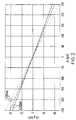
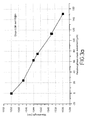
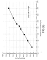
- Figures 3a. 3b, 4a and 4b illustrate empirical results obtained with a prototype device according to Figure 1.
- Figure 3a shows a tuning range from 1535.5 nm to 1550 nm with a slope of 0.94nm/10 ⁇ m obtained by moving the phase-mask and keeping the lens in a fixed position.
- Figure 3b shows a tuning range from 1522 nm to 1549 nm with a slope of 0.92 nm/10 ⁇ m obtained by moving the lens and for fixed phase-mask position.
- Figures 4a and 4b illustrate empirical reflection and time delay characteristics of a linearly chirped fibre grating written with the interferometer of Figure 1.
- the grating is 85 cm long has a 3 nm bandwidth and is written using 100 mW of CW UV-light from a frequency doubled Ar-ion laser.
- the grating is written in a D 2 -loaded high NA (0.2) fibre.
- the advantage of using a bi-convex lens to catch and recombine the diffracted orders from the phase mask is that it is known as the 'best form' for 1:1 imaging. This because it does not introduce any aberrations. Furthermore the embodiment is simple and robust it employs only one lens element within the interferometer. Moreover, by blocking the transmitted 0th order beam from the phase mask a better visibility is obtained in the interference pattern between the interfering -1 and 1 orders.
- the apparatus lends itself to use with a system such as that described in GB9617688.8, namely a technique involving fabricating an optical waveguide grating having a plurality of grating lines of refractive index variation, the and comprising the steps of:
- the apparatus and methods described earlier can easily be used to provide a writing light beam of varying grating pitch.
- the movement between the writing beams and the waveguide can be achieved by one or more translation stages or possibly by tilting the lens 60.
Landscapes
- Physics & Mathematics (AREA)
- Engineering & Computer Science (AREA)
- General Physics & Mathematics (AREA)
- Optics & Photonics (AREA)
- Manufacturing & Machinery (AREA)
- Microelectronics & Electronic Packaging (AREA)
- Diffracting Gratings Or Hologram Optical Elements (AREA)
- Optical Fibers, Optical Fiber Cores, And Optical Fiber Bundles (AREA)
- Optical Integrated Circuits (AREA)
Claims (9)
- Dispositif de fabrication de réseau optique comprenant :un masque de phase (40) pour diviser un faisceau de lumière incidente en une pluralité de faisceaux diffractés ;un dispositif de focalisation (60) destiné à recevoir la lumière du masque de phase et à faire converger au moins deux faisceaux diffractés d'ordre non nul afin de créer une région d'interférence de période caractéristique entre les faisceaux convergents, de sorte qu'une structure de réseau peut être imprimée sur un guide d'onde optique (80) placé dans la région d'interférence ;et un appareil de translation pour fournir une translation relative du dispositif de fabrication de réseau et d'un guide d'onde optique dans lequel un réseau doit être fabriqué, de sorte que la région d'interférence peut être incidente sur différentes parties du guide d'onde optique ;caractérisé par un étage de translation (90) adapté pour déplacer le masque de phase et au moins une partie du dispositif de focalisation l'un par rapport à l'autre ; et
un circuit de commande (100) adapté pour modifier la séparation relative du masque de phase et de ladite au moins une partie du dispositif de focalisation pendant que le guide d'onde est déplacé par rapport à la région d'interférence afin de modifier l'angle de convergence des faisceaux convergents et d'accorder ainsi de manière contrôlée la période caractéristique. - Dispositif selon la revendication 1, dans lequel le dispositif de focalisation est constitué d'une seul lentille.
- Dispositif selon la revendication 2, dans lequel la lentille est une lentille sphérique biconvexe.
- Dispositif selon l'une quelconque des revendications 1 à 3, comprenant un dispositif de collimation pour collimater substantiellement le faisceau arrivant sur le masque de phase.
- Dispositif selon la revendication 4 lorsqu'elle dépend de la revendication 2 ou 3, dans lequel le dispositif de collimation comprend une lentille (20) dont la distance focale est le double de celle de la lentille du dispositif de focalisation.
- Dispositif selon l'une quelconque des revendications précédentes, dans lequel le guide d'onde est un guide d'onde à fibre optique.
- Dispositif selon l'une quelconque des revendications précédentes, le dispositif comprenant un moyen permettant d'exposer de manière répétée la région d'interférence sur le guide d'onde ; dans lequel l'appareil de translation est utilisable pour déplacer la région d'interférence et/ou le guide d'onde entre les expositions successives du motif de lumière d'écriture, de sorte que chacune d'au moins une majorité des lignes de réseau du réseau de guide d'onde est générée par au moins deux expositions à la région d'interférence.
- Procédé de fabrication d'un réseau optique comprenant les étapes consistant à :diriger un faisceau lumineux sur un masque de phase (40) pour diviser le faisceau lumineux en une pluralité de faisceaux diffractés ;faire converger au moins deux faisceaux diffractés d'ordre non nul en employant un dispositif de focalisation (60) afin de générer une région d'interférence de période caractéristique entre les faisceaux convergents, de sorte qu'une structure de réseau peut être imprimée sur un guide d'onde optique placé dans la région d'interférence ; etdéplacer le guide d'onde par rapport à la région d'interférence, caractérisé par l'étape consistant à :provoquer un déplacement relatif entre le masque de phase et au moins une partie du dispositif de focalisation pour modifier leur séparation relative afin de modifier l'angle de convergence des faisceaux convergents et d'accorder la période caractéristique sur une période souhaitée pendant que le guide d'onde optique est déplacé par rapport à la région d'interférence pour fabriquer un réseau à pas variable.
- Procédé selon la revendication 8, dans lequel l'étape consistant à diriger le faisceau lumineux sur le masque de phase comprend le fait de collimater le faisceau lumineux avec une lentille (20) dont la distance focale est le double de celle du dispositif de focalisation.
Applications Claiming Priority (3)
| Application Number | Priority Date | Filing Date | Title |
|---|---|---|---|
| GB9722550 | 1997-10-24 | ||
| GBGB9722550.2A GB9722550D0 (en) | 1997-10-24 | 1997-10-24 | Fabrication of optical waveguide gratings |
| PCT/GB1998/003176 WO1999022256A1 (fr) | 1997-10-24 | 1998-10-23 | Fabrication de reseaux pour guides d'ondes optiques |
Publications (2)
| Publication Number | Publication Date |
|---|---|
| EP1025457A1 EP1025457A1 (fr) | 2000-08-09 |
| EP1025457B1 true EP1025457B1 (fr) | 2007-02-21 |
Family
ID=10821085
Family Applications (1)
| Application Number | Title | Priority Date | Filing Date |
|---|---|---|---|
| EP98949145A Expired - Lifetime EP1025457B1 (fr) | 1997-10-24 | 1998-10-23 | Fabrication de reseaux pour guides d'ondes optiques |
Country Status (13)
| Country | Link |
|---|---|
| US (1) | US6549705B1 (fr) |
| EP (1) | EP1025457B1 (fr) |
| JP (1) | JP4512266B2 (fr) |
| KR (1) | KR20010031375A (fr) |
| CN (1) | CN1135412C (fr) |
| AR (1) | AR017388A1 (fr) |
| AU (1) | AU731754B2 (fr) |
| BR (1) | BR9813267B1 (fr) |
| CA (1) | CA2307189C (fr) |
| DE (1) | DE69837157D1 (fr) |
| GB (1) | GB9722550D0 (fr) |
| NZ (1) | NZ504184A (fr) |
| WO (1) | WO1999022256A1 (fr) |
Families Citing this family (33)
| Publication number | Priority date | Publication date | Assignee | Title |
|---|---|---|---|---|
| EP1139123A1 (fr) * | 2000-03-30 | 2001-10-04 | Optical Technologies Italia S.p.A. | Procédé et appareil pour l'inscription d'un réseau de Bragg dans un guide d'ondes |
| US6553163B2 (en) | 2000-03-30 | 2003-04-22 | Corning, Incorporated | Method and apparatus for writing a Bragg grating in a waveguide |
| KR100342493B1 (ko) * | 2000-07-25 | 2002-06-28 | 윤종용 | 회절 효과를 최소화하기 위한 광섬유 격자 제작장치 |
| AUPR134500A0 (en) * | 2000-11-08 | 2000-11-30 | Redfern Optical Components Pty Ltd | Interferometer for writing bragg gratings |
| US6778733B2 (en) * | 2001-01-05 | 2004-08-17 | Teraxion Inc. | Lithographic fabrication of phase mask for fiber Bragg gratings |
| US6898350B2 (en) * | 2001-01-18 | 2005-05-24 | General Dynamics Advanced Information Systems, Inc. | Interferometric focusing technique for forming taps in fibers |
| SE520909C2 (sv) * | 2001-03-08 | 2003-09-09 | Proximion Fiber Optics Ab | Metod och anordning för fotoinducering av ett lutat gitter i en optisk fiber |
| NO314677B1 (no) | 2001-06-29 | 2003-04-28 | Optoplan As | FBG produksjonssystem |
| CA2377208A1 (fr) * | 2001-10-09 | 2003-04-09 | Teraxion Inc. | Methode et appareil d'enregistrement de reseaux optiques sur un support photosensible |
| US6873762B1 (en) | 2002-04-08 | 2005-03-29 | The United States Of America As Represented By The Administrator Of The National Aeronautics And Space Administration | Fabrication of fiber optic grating apparatus and method |
| AUPS253202A0 (en) * | 2002-05-23 | 2002-06-13 | University Of Sydney, The | Interferometric grating writing methods and apparatus |
| US6751381B1 (en) | 2002-05-24 | 2004-06-15 | Teraxion Inc. | Embodying amplitude information into phase masks |
| KR100442879B1 (ko) * | 2002-07-18 | 2004-08-02 | 삼성전자주식회사 | 목표 패턴에 최적화된 변형 조명을 제공하는 위상 격자패턴 설계 방법 및 이를 이용한 포토 마스크 제조 방법 |
| GB0217047D0 (en) * | 2002-07-23 | 2002-08-28 | Univ Southampton | Optically induced refractive index modification in optical materials |
| US6904202B1 (en) * | 2002-07-31 | 2005-06-07 | Intel Corporation | Writing waveguides with an arbitrary Bragg wavelength |
| GB2395797A (en) * | 2002-11-28 | 2004-06-02 | Univ Southampton | Fabrication of optical waveguides and Bragg gratings |
| AU2003900836A0 (en) | 2003-02-25 | 2003-03-13 | Redfern Optical Components Pty Ltd | Optical structure writing system |
| US6853772B2 (en) * | 2003-05-13 | 2005-02-08 | 3M Innovative Properties Company | Fiber grating writing interferometer with continuous wavelength tuning and chirp capability |
| JP2005055508A (ja) * | 2003-08-05 | 2005-03-03 | Fujikura Ltd | グレーティング型光部品製造方法、グレーティング型光部品製造装置、グレーティング型光部品製造方法又はグレーティング型光部品製造装置を用いて作製された光部品 |
| US7274358B2 (en) * | 2004-01-06 | 2007-09-25 | Tyco Electronics Corporation | Focusing-shaped reflector arrays for acoustic touchscreens |
| CN100434944C (zh) * | 2006-05-25 | 2008-11-19 | 中国科学院长春光学精密机械与物理研究所 | 一种光栅刻划机的载物滑座减重同步移动机构 |
| WO2008010790A1 (fr) * | 2006-07-18 | 2008-01-24 | Celloptic, Inc. | Système, appareil et procédé pour extraire des informations tridimensionnelles d'un objet depuis un rayonnement électromagnétique reçu |
| KR100782879B1 (ko) * | 2006-12-07 | 2007-12-06 | 한국전자통신연구원 | 광섬유 브래그 격자 제조 장치 및 그 장치로 제조된 브래그격자를 갖는 광섬유 및 중적외선 광섬유 레이저 |
| US7944598B2 (en) * | 2008-11-06 | 2011-05-17 | Corning Incorporated | Speckle mitigation in laser scanner projector systems |
| CN102221727B (zh) * | 2011-07-18 | 2012-11-07 | 武汉理工大学 | 实现一次曝光的切趾装置及方法 |
| CN105806379B (zh) * | 2014-12-30 | 2019-03-12 | 深圳先进技术研究院 | 弱反射光纤布拉格光栅-珐泊腔传感器的解调系统 |
| DE102015216342B3 (de) * | 2015-08-26 | 2016-12-22 | Laser-Laboratorium Göttingen e.V. | Technik zur Herstellung periodischer Strukturen |
| CN106980224A (zh) * | 2016-01-19 | 2017-07-25 | 香港理工大学 | 一种相位掩模板以及光纤光栅的制造设备及方法 |
| CN106772822B (zh) * | 2017-01-20 | 2019-08-16 | 深圳大学 | 一种高速光开关器件 |
| US10222615B2 (en) * | 2017-05-26 | 2019-03-05 | Microsoft Technology Licensing, Llc | Optical waveguide with coherent light source |
| CN111492304B (zh) * | 2017-12-26 | 2022-02-25 | 三菱电机株式会社 | 光图案生成装置 |
| CN108732677A (zh) * | 2018-05-25 | 2018-11-02 | 南京理工大学 | 一种宽带宽高斯型低反光纤光栅的刻写方法 |
| CN110187424B (zh) * | 2019-05-05 | 2021-06-01 | 中国科学院上海光学精密机械研究所 | 皮米光梳、皮米光梳的制造装置和制造方法 |
Family Cites Families (17)
| Publication number | Priority date | Publication date | Assignee | Title |
|---|---|---|---|---|
| US5367588A (en) * | 1992-10-29 | 1994-11-22 | Her Majesty The Queen In Right Of Canada, As Represented By The Minister Of Communications | Method of fabricating Bragg gratings using a silica glass phase grating mask and mask used by same |
| US5104209A (en) * | 1991-02-19 | 1992-04-14 | Her Majesty The Queen In Right Of Canada, As Represented By The Minister Of Communications | Method of creating an index grating in an optical fiber and a mode converter using the index grating |
| US5328785A (en) * | 1992-02-10 | 1994-07-12 | Litel Instruments | High power phase masks for imaging systems |
| JPH0611609A (ja) * | 1992-06-26 | 1994-01-21 | Matsushita Electric Ind Co Ltd | 露光装置 |
| US5327515A (en) * | 1993-01-14 | 1994-07-05 | At&T Laboratories | Method for forming a Bragg grating in an optical medium |
| GB2289771B (en) * | 1994-05-26 | 1997-07-30 | Northern Telecom Ltd | Forming Bragg gratings in photosensitive waveguides |
| JPH0829631A (ja) * | 1994-07-13 | 1996-02-02 | Nippon Telegr & Teleph Corp <Ntt> | チャープグレーティング作製装置 |
| FR2728356B1 (fr) * | 1994-12-15 | 1997-01-31 | Alcatel Fibres Optiques | Dispositif d'impression d'un reseau de bragg dans une fibre optique |
| JPH08286009A (ja) * | 1995-04-13 | 1996-11-01 | Sumitomo Electric Ind Ltd | チャープ格子形成装置 |
| JPH08286059A (ja) * | 1995-04-13 | 1996-11-01 | Sumitomo Electric Ind Ltd | チャープ格子形成装置 |
| FR2742881B1 (fr) * | 1995-12-26 | 1998-02-06 | Alsthom Cge Alcatel | Procede et systeme d'inscription point par point d'un reseau de bragg dans une fibre optique |
| TW358167B (en) * | 1996-03-25 | 1999-05-11 | Corning Inc | Method of forming a grating in an optical waveguide |
| JPH09265017A (ja) * | 1996-03-28 | 1997-10-07 | Sumitomo Electric Ind Ltd | グレーティング作成装置 |
| GB2316760A (en) | 1996-08-23 | 1998-03-04 | Univ Southampton | Fabricating optical waveguide gratings |
| US5945261A (en) * | 1996-11-19 | 1999-08-31 | Northern Telecom Limited | Creation of Bragg reflective gratings in waveguides |
| JP2985820B2 (ja) * | 1997-02-14 | 1999-12-06 | 日立電線株式会社 | 低反射グレーティングが形成された光導波路及びその製造方法 |
| EP1145149B1 (fr) * | 1998-11-13 | 2005-04-06 | Cellomics, Inc. | Procedes et systeme de collection et de stockage efficaces de donnees experimentales |
-
1997
- 1997-10-24 GB GBGB9722550.2A patent/GB9722550D0/en not_active Ceased
-
1998
- 1998-10-23 CA CA002307189A patent/CA2307189C/fr not_active Expired - Lifetime
- 1998-10-23 KR KR1020007004383A patent/KR20010031375A/ko not_active Withdrawn
- 1998-10-23 AU AU95519/98A patent/AU731754B2/en not_active Expired
- 1998-10-23 CN CNB988117037A patent/CN1135412C/zh not_active Expired - Lifetime
- 1998-10-23 NZ NZ504184A patent/NZ504184A/xx not_active IP Right Cessation
- 1998-10-23 EP EP98949145A patent/EP1025457B1/fr not_active Expired - Lifetime
- 1998-10-23 DE DE69837157T patent/DE69837157D1/de not_active Expired - Lifetime
- 1998-10-23 WO PCT/GB1998/003176 patent/WO1999022256A1/fr not_active Ceased
- 1998-10-23 BR BRPI9813267-9A patent/BR9813267B1/pt not_active IP Right Cessation
- 1998-10-23 JP JP2000518294A patent/JP4512266B2/ja not_active Expired - Lifetime
- 1998-10-26 AR ARP980105328A patent/AR017388A1/es not_active Application Discontinuation
-
2000
- 2000-04-21 US US09/556,828 patent/US6549705B1/en not_active Expired - Lifetime
Also Published As
| Publication number | Publication date |
|---|---|
| JP2001521203A (ja) | 2001-11-06 |
| BR9813267B1 (pt) | 2011-12-13 |
| CA2307189A1 (fr) | 1999-05-06 |
| JP4512266B2 (ja) | 2010-07-28 |
| DE69837157D1 (de) | 2007-04-05 |
| KR20010031375A (ko) | 2001-04-16 |
| CN1135412C (zh) | 2004-01-21 |
| CN1280677A (zh) | 2001-01-17 |
| AU9551998A (en) | 1999-05-17 |
| BR9813267A (pt) | 2000-08-22 |
| GB9722550D0 (en) | 1997-12-24 |
| AU731754B2 (en) | 2001-04-05 |
| CA2307189C (fr) | 2007-08-07 |
| WO1999022256A1 (fr) | 1999-05-06 |
| AR017388A1 (es) | 2001-09-05 |
| NZ504184A (en) | 2002-11-26 |
| EP1025457A1 (fr) | 2000-08-09 |
| US6549705B1 (en) | 2003-04-15 |
Similar Documents
| Publication | Publication Date | Title |
|---|---|---|
| EP1025457B1 (fr) | Fabrication de reseaux pour guides d'ondes optiques | |
| JP4177893B2 (ja) | 光導波管格子 | |
| US6307679B1 (en) | Formation of a refractive index grating | |
| EP0960347B1 (fr) | Masque de phase presentant une efficacite de diffraction variable dans l'espace | |
| US6753118B2 (en) | Optical grating fabrication process | |
| US10156680B2 (en) | Forming an optical grating with an apparatus providing an adjustable interference pattern | |
| JPH06235808A (ja) | 光媒体にブラッグ回折格子を形成する方法 | |
| US6130973A (en) | Method and apparatus for spectrally designing all-fiber filters | |
| WO2003032038A1 (fr) | Procede et appareil d'enregistrement d'un reseau optique sur un support photosensible | |
| US6553163B2 (en) | Method and apparatus for writing a Bragg grating in a waveguide | |
| GB2300932A (en) | Phase grating mask for making Bragg gratings in optical waveguides | |
| US6501883B1 (en) | Method and apparatus for recording an optical grating in a photosensitive medium | |
| US6778733B2 (en) | Lithographic fabrication of phase mask for fiber Bragg gratings | |
| JP3168194B2 (ja) | オフセット等価ミラー面を有するファイバーブラッググレーティング及びその製造方法 | |
| JP3346440B2 (ja) | 透過型ファイバグレーティングフィルタの製造方法 | |
| JP2004538497A (ja) | 導波路にブラッググレーティングを書き込む方法及び装置 | |
| CA2281787C (fr) | Masque de phase presentant une efficacite de diffraction variable dans l'espace | |
| JP4543128B2 (ja) | 光導波路ブラッググレーティングの製造方法および製造装置 | |
| JP3281349B2 (ja) | 光ファイバー格子の製造方法及び装置 | |
| CA2230200C (fr) | Methode et appareil de conception spectrale de filtres fibreux | |
| Voigtländer et al. | Variable period change of femtosecond written fiber Bragg gratings with a deformed wavefront | |
| Ashton et al. | Two-point source grating writing methods | |
| JP4279227B2 (ja) | 光導波路ブラッググレーティングの製造方法および製造装置 | |
| JP2006099011A5 (fr) | ||
| Floreani et al. | A simple method for the fabrication of intrinsically apodized chirped fibre Bragg gratings |
Legal Events
| Date | Code | Title | Description |
|---|---|---|---|
| PUAI | Public reference made under article 153(3) epc to a published international application that has entered the european phase |
Free format text: ORIGINAL CODE: 0009012 |
|
| 17P | Request for examination filed |
Effective date: 20000509 |
|
| AK | Designated contracting states |
Kind code of ref document: A1 Designated state(s): DE ES FR GB IT |
|
| 17Q | First examination report despatched |
Effective date: 20000915 |
|
| RAP1 | Party data changed (applicant data changed or rights of an application transferred) |
Owner name: PIRELLI S.P.A. |
|
| RAP1 | Party data changed (applicant data changed or rights of an application transferred) |
Owner name: PIRELLI & C. S.P.A. |
|
| GRAP | Despatch of communication of intention to grant a patent |
Free format text: ORIGINAL CODE: EPIDOSNIGR1 |
|
| GRAS | Grant fee paid |
Free format text: ORIGINAL CODE: EPIDOSNIGR3 |
|
| RIC1 | Information provided on ipc code assigned before grant |
Ipc: G02B 6/34 20060101ALI20061201BHEP Ipc: G02B 6/124 20060101ALI20061201BHEP Ipc: G02B 6/00 20060101AFI20061201BHEP |
|
| GRAA | (expected) grant |
Free format text: ORIGINAL CODE: 0009210 |
|
| AK | Designated contracting states |
Kind code of ref document: B1 Designated state(s): DE ES FR GB IT |
|
| REG | Reference to a national code |
Ref country code: GB Ref legal event code: FG4D |
|
| REF | Corresponds to: |
Ref document number: 69837157 Country of ref document: DE Date of ref document: 20070405 Kind code of ref document: P |
|
| PG25 | Lapsed in a contracting state [announced via postgrant information from national office to epo] |
Ref country code: ES Free format text: LAPSE BECAUSE OF FAILURE TO SUBMIT A TRANSLATION OF THE DESCRIPTION OR TO PAY THE FEE WITHIN THE PRESCRIBED TIME-LIMIT Effective date: 20070601 |
|
| EN | Fr: translation not filed | ||
| PLBE | No opposition filed within time limit |
Free format text: ORIGINAL CODE: 0009261 |
|
| STAA | Information on the status of an ep patent application or granted ep patent |
Free format text: STATUS: NO OPPOSITION FILED WITHIN TIME LIMIT |
|
| 26N | No opposition filed |
Effective date: 20071122 |
|
| PG25 | Lapsed in a contracting state [announced via postgrant information from national office to epo] |
Ref country code: DE Free format text: LAPSE BECAUSE OF FAILURE TO SUBMIT A TRANSLATION OF THE DESCRIPTION OR TO PAY THE FEE WITHIN THE PRESCRIBED TIME-LIMIT Effective date: 20070522 |
|
| PG25 | Lapsed in a contracting state [announced via postgrant information from national office to epo] |
Ref country code: FR Free format text: LAPSE BECAUSE OF FAILURE TO SUBMIT A TRANSLATION OF THE DESCRIPTION OR TO PAY THE FEE WITHIN THE PRESCRIBED TIME-LIMIT Effective date: 20071012 |
|
| PG25 | Lapsed in a contracting state [announced via postgrant information from national office to epo] |
Ref country code: FR Free format text: LAPSE BECAUSE OF FAILURE TO SUBMIT A TRANSLATION OF THE DESCRIPTION OR TO PAY THE FEE WITHIN THE PRESCRIBED TIME-LIMIT Effective date: 20070221 |
|
| PGFP | Annual fee paid to national office [announced via postgrant information from national office to epo] |
Ref country code: GB Payment date: 20171027 Year of fee payment: 20 Ref country code: IT Payment date: 20171024 Year of fee payment: 20 |
|
| REG | Reference to a national code |
Ref country code: GB Ref legal event code: PE20 Expiry date: 20181022 |
|
| PG25 | Lapsed in a contracting state [announced via postgrant information from national office to epo] |
Ref country code: GB Free format text: LAPSE BECAUSE OF EXPIRATION OF PROTECTION Effective date: 20181022 |