EP0965255B2 - Procede pour fabriquer un boitier de blindage - Google Patents
Procede pour fabriquer un boitier de blindage Download PDFInfo
- Publication number
- EP0965255B2 EP0965255B2 EP98919059A EP98919059A EP0965255B2 EP 0965255 B2 EP0965255 B2 EP 0965255B2 EP 98919059 A EP98919059 A EP 98919059A EP 98919059 A EP98919059 A EP 98919059A EP 0965255 B2 EP0965255 B2 EP 0965255B2
- Authority
- EP
- European Patent Office
- Prior art keywords
- enclosure
- profile
- screening
- sealing
- strand
- Prior art date
- Legal status (The legal status is an assumption and is not a legal conclusion. Google has not performed a legal analysis and makes no representation as to the accuracy of the status listed.)
- Expired - Lifetime
Links
- 238000004519 manufacturing process Methods 0.000 title claims abstract description 13
- 239000000463 material Substances 0.000 claims abstract description 71
- 238000007789 sealing Methods 0.000 claims abstract description 33
- 238000000034 method Methods 0.000 claims abstract description 16
- 238000012216 screening Methods 0.000 claims abstract 15
- 229910052751 metal Inorganic materials 0.000 claims description 14
- 239000002184 metal Substances 0.000 claims description 14
- 230000000694 effects Effects 0.000 claims description 10
- 239000004033 plastic Substances 0.000 claims description 10
- 229920003023 plastic Polymers 0.000 claims description 10
- 239000000956 alloy Substances 0.000 claims description 6
- 229910045601 alloy Inorganic materials 0.000 claims description 6
- 229910052709 silver Inorganic materials 0.000 claims description 6
- 239000004332 silver Substances 0.000 claims description 6
- 239000002245 particle Substances 0.000 claims description 5
- 229920001296 polysiloxane Polymers 0.000 claims description 5
- 239000000919 ceramic Substances 0.000 claims description 3
- 235000011837 pasties Nutrition 0.000 claims description 3
- 230000009974 thixotropic effect Effects 0.000 claims description 2
- 239000000945 filler Substances 0.000 claims 2
- 239000012811 non-conductive material Substances 0.000 claims 1
- 239000013013 elastic material Substances 0.000 abstract description 3
- 238000001723 curing Methods 0.000 description 9
- 239000007858 starting material Substances 0.000 description 6
- 239000004020 conductor Substances 0.000 description 5
- 239000010410 layer Substances 0.000 description 5
- PXHVJJICTQNCMI-UHFFFAOYSA-N Nickel Chemical compound [Ni] PXHVJJICTQNCMI-UHFFFAOYSA-N 0.000 description 4
- BQCADISMDOOEFD-UHFFFAOYSA-N Silver Chemical compound [Ag] BQCADISMDOOEFD-UHFFFAOYSA-N 0.000 description 3
- 238000000576 coating method Methods 0.000 description 3
- 238000004132 cross linking Methods 0.000 description 3
- 239000011159 matrix material Substances 0.000 description 3
- 239000000203 mixture Substances 0.000 description 3
- 239000000843 powder Substances 0.000 description 3
- 230000001588 bifunctional effect Effects 0.000 description 2
- 239000011248 coating agent Substances 0.000 description 2
- 238000010276 construction Methods 0.000 description 2
- 238000005260 corrosion Methods 0.000 description 2
- 230000007797 corrosion Effects 0.000 description 2
- 238000011161 development Methods 0.000 description 2
- 230000018109 developmental process Effects 0.000 description 2
- KPUWHANPEXNPJT-UHFFFAOYSA-N disiloxane Chemical class [SiH3]O[SiH3] KPUWHANPEXNPJT-UHFFFAOYSA-N 0.000 description 2
- 230000005670 electromagnetic radiation Effects 0.000 description 2
- 229910052759 nickel Inorganic materials 0.000 description 2
- 238000002360 preparation method Methods 0.000 description 2
- 238000010079 rubber tapping Methods 0.000 description 2
- 238000005507 spraying Methods 0.000 description 2
- 239000002344 surface layer Substances 0.000 description 2
- 229920001187 thermosetting polymer Polymers 0.000 description 2
- RYGMFSIKBFXOCR-UHFFFAOYSA-N Copper Chemical compound [Cu] RYGMFSIKBFXOCR-UHFFFAOYSA-N 0.000 description 1
- 229920002430 Fibre-reinforced plastic Polymers 0.000 description 1
- 239000004594 Masterbatch (MB) Substances 0.000 description 1
- 229910004298 SiO 2 Inorganic materials 0.000 description 1
- 229910052782 aluminium Inorganic materials 0.000 description 1
- XAGFODPZIPBFFR-UHFFFAOYSA-N aluminium Chemical compound [Al] XAGFODPZIPBFFR-UHFFFAOYSA-N 0.000 description 1
- 238000000429 assembly Methods 0.000 description 1
- 230000000712 assembly Effects 0.000 description 1
- 230000004888 barrier function Effects 0.000 description 1
- 230000015572 biosynthetic process Effects 0.000 description 1
- 239000007767 bonding agent Substances 0.000 description 1
- 150000001875 compounds Chemical class 0.000 description 1
- 230000006835 compression Effects 0.000 description 1
- 238000007906 compression Methods 0.000 description 1
- 239000011231 conductive filler Substances 0.000 description 1
- 229910052802 copper Inorganic materials 0.000 description 1
- 239000010949 copper Substances 0.000 description 1
- 238000005336 cracking Methods 0.000 description 1
- 238000010586 diagram Methods 0.000 description 1
- 238000009792 diffusion process Methods 0.000 description 1
- 239000000428 dust Substances 0.000 description 1
- 229920001971 elastomer Polymers 0.000 description 1
- 239000000806 elastomer Substances 0.000 description 1
- 238000009713 electroplating Methods 0.000 description 1
- 239000000835 fiber Substances 0.000 description 1
- 239000011151 fibre-reinforced plastic Substances 0.000 description 1
- 238000013023 gasketing Methods 0.000 description 1
- 239000011521 glass Substances 0.000 description 1
- 238000012423 maintenance Methods 0.000 description 1
- 238000001465 metallisation Methods 0.000 description 1
- 239000002991 molded plastic Substances 0.000 description 1
- 229920001084 poly(chloroprene) Polymers 0.000 description 1
- 238000009417 prefabrication Methods 0.000 description 1
- 230000035755 proliferation Effects 0.000 description 1
- 238000003847 radiation curing Methods 0.000 description 1
- 229920005989 resin Polymers 0.000 description 1
- 239000011347 resin Substances 0.000 description 1
- 239000003566 sealing material Substances 0.000 description 1
- 150000004760 silicates Chemical class 0.000 description 1
- 229920002050 silicone resin Polymers 0.000 description 1
- 229920002379 silicone rubber Polymers 0.000 description 1
- 239000004945 silicone rubber Substances 0.000 description 1
- 239000011343 solid material Substances 0.000 description 1
- 239000000758 substrate Substances 0.000 description 1
- 238000004381 surface treatment Methods 0.000 description 1
- 239000004094 surface-active agent Substances 0.000 description 1
- 238000012360 testing method Methods 0.000 description 1
- 238000007740 vapor deposition Methods 0.000 description 1
Images

Classifications
-
- H—ELECTRICITY
- H05—ELECTRIC TECHNIQUES NOT OTHERWISE PROVIDED FOR
- H05K—PRINTED CIRCUITS; CASINGS OR CONSTRUCTIONAL DETAILS OF ELECTRIC APPARATUS; MANUFACTURE OF ASSEMBLAGES OF ELECTRICAL COMPONENTS
- H05K9/00—Screening of apparatus or components against electric or magnetic fields
-
- H—ELECTRICITY
- H05—ELECTRIC TECHNIQUES NOT OTHERWISE PROVIDED FOR
- H05K—PRINTED CIRCUITS; CASINGS OR CONSTRUCTIONAL DETAILS OF ELECTRIC APPARATUS; MANUFACTURE OF ASSEMBLAGES OF ELECTRICAL COMPONENTS
- H05K9/00—Screening of apparatus or components against electric or magnetic fields
- H05K9/0007—Casings
- H05K9/0015—Gaskets or seals
-
- Y—GENERAL TAGGING OF NEW TECHNOLOGICAL DEVELOPMENTS; GENERAL TAGGING OF CROSS-SECTIONAL TECHNOLOGIES SPANNING OVER SEVERAL SECTIONS OF THE IPC; TECHNICAL SUBJECTS COVERED BY FORMER USPC CROSS-REFERENCE ART COLLECTIONS [XRACs] AND DIGESTS
- Y10—TECHNICAL SUBJECTS COVERED BY FORMER USPC
- Y10T—TECHNICAL SUBJECTS COVERED BY FORMER US CLASSIFICATION
- Y10T156/00—Adhesive bonding and miscellaneous chemical manufacture
- Y10T156/17—Surface bonding means and/or assemblymeans with work feeding or handling means
- Y10T156/1798—Surface bonding means and/or assemblymeans with work feeding or handling means with liquid adhesive or adhesive activator applying means
Definitions
- the invention relates to a method for producing a shielding housing according to the preamble of claim 1, and to an electrically conductive seal according to the preamble of claim 10.
- housings used to be mostly made of metal for obvious reasons, cost and weight reasons have been overcome with the onset of their proliferation - for example, in cell phones or cordless telephones - in particular to manufacture them from plastic.
- the prefabricated, in particular injection-molded, housing parts are coated with a conductive material, such as by spraying conductive ink, vapor deposition with aluminum or electroplating.
- Such housings were initially usually provided with prefabricated seals, which consist of conductive elastomer and are inserted during assembly.
- DE 38 12 943 A1 shows an internally coated shielding made of fiber-reinforced plastic with such a prefabricated, inserted between tongue and groove seal.
- the housings described therein are composed of two parts which are made (or at least partially) of electrically conductive material for electrical shielding of the housing interior or are coated with such and form a Faraday cage in the assembled state.
- a shielding seal is provided, which consists of an electrically conductive and elastic material and adapts to surface tolerances and bumps, so that even in mass production a very high quality of the shielding of the housing interior are guaranteed can.
- This shielding gasket is made directly on at least one of the housing parts, wherein an additional support may be included in the structure.
- the housing can be opened, for example, for maintenance purposes or to replace an energy source and then - while maintaining the sealing and shielding effect - again close easily.
- a material with advantageously high shielding effect is a filled with a high proportion of silver powder plastic mass, but this is relatively expensive and has only partially satisfactory mechanical properties.
- the invention is therefore based on the object to provide a method for producing a shielding of the type mentioned, which allows a simple and cost-effective production of shielding with very good mechanical and electromagnetic properties and long life.
- Claim 10 relates to a housing part of a shielding housing with an electrically conductive seal according to the invention.
- the invention includes the technical teaching to form the Ableprofil in a single application step of (at least) two different, elastically curing, but optimized for different functions components such that they are firmly and permanently connected to each other and thus form a reliable bifunctional unit ,
- both components can be applied to the housing with high process speed in sufficient thickness for an excellent sealing or shielding effect. Since the surfaces of both components in the initial state, ie before the onset of any crosslinking or curing, are brought into contact with each other, they crosslink with each other or a diffusion barrier layer is formed, which ensures a practically insoluble connection of both profile parts.
- the profiled part or section formed from the first material primarily has the function of filling the gap between the joints in order reliably to protect the housing interior against moisture and dust despite a mechanical play of the housing parts caused by manufacturing tolerances or asperities and, if necessary, to prevent relative movements between the housing parts , Due to the mechanically optimized properties of the first material, it is possible to permanently hermetically seal the housing interior.
- the first one Profile part carries a portion of the electromagnetic shielding and secures its closure.
- a plastic material made conductive by electrically conductive inclusions of the same type as the first material is used as the second material.
- the achieved thereby substantial material uniformity serves to deepen the above-mentioned effect.
- Ableukin-based a luftumd room temperature-curing and in particular thixotropic properties having plastic material, especially on silicone-based, in advantageous. Technologically simplified and cheaper, but alternatively also thermosetting or radiation-crosslinking material can be used.
- Particles of a metal or an alloy having high electrical conductivity, in particular silver or a silver-containing alloy are added as electrically conductive inclusions to achieve a shielding effect which meets the high test requirements.
- the use of a silver-plated powder of another metal (nickel, copper or the like) or of non-conductive carrier particles (for example of glass) is more cost-effective.
- the metal content is typically over 25% by mass, to achieve the highest shielding effects in mobile phones, etc. possibly even significantly above 50% by mass, based on the mass of the silicone-metal mixture.
- metal short fibers or platelets which can advantageously form a type of metal framework in the plastic matrix with suitable specification of their dimensions in coordination with the properties of the matrix material and the process parameters. This can give the conductive profile part a high conductivity at relatively low metal content and in conjunction with this at the same time lead to advantages in terms of a relatively low hardness and brittleness.
- a non-conductive filler in particular a cost oxidic or ceramic powder (SiO 2 , silicates or the like) may be added to the first material.
- a bonding agent can be used to increase the adhesion to this when applying the first and / or second material; Alternatively, however, it can also be applied in advance, for example in the course of surface treatment of the housing parts.
- the second housing part is preferably brought into contact with the sealing and shielding profile only after substantially complete curing of the first and / or second material.
- an application needle / nozzle is used when the sealing and shielding profile is applied, in which case the first channel is completely surrounded by the second channel.
- an applicator needle or nozzle can be used, the first channel has a substantially circular cross-section and is surrounded concentrically by the second channel, wherein this has a substantially annular segment-shaped cross-section.
- Needle shape and cross-section are chosen in a preferred embodiment for many applications so that the second material is applied in the profile cross-section with uneven thickness.
- the second material can be applied on the inside of the housing with a greater thickness than in the portion facing a housing part and / or on the outside of the housing, whereby a tendentially "softer" seal can be realized.
- problems can be counteracted, which may result from a possible corrosion of the metal filling of the second material, especially in extreme fields of use (tropics, ocean shipping, etc.).
- the shielding profile is constructed by simultaneous application of three material strands in sandwich construction from a three-channel needle by applying two strands of mechanically optimized type material ("first material”) and a strand of electrically conductive material between them. which causes the electromagnetic shielding.
- first material mechanically optimized type material
- the arrangement of the profile part consisting of electrically conductive material in an essentially deformation-free region between two deformable layers or strands of the elastic element advantageously counteracts cracking in the electrically conductive material, which is of particular importance for structures in which a high degree of deformation is involved of the shielding can occur during assembly of the housing parts. This arrangement is also particularly resistant to corrosion.
- a crosslinkable, crosslinking-curing silicone rubber to form a gel-like state, a long-chain, pronouncevernetzendes Siloxane be admixed.
- the sealing and shielding profile formed from such a mixture is characterized by high adhesion to the substrate as well as a Shore A hardness which can be set to low values and a high possible degree of deformation.
- Relatively soft and yet mechanically sufficiently resistant EMI shielding profiles can be produced with materials containing about 5% by weight of bifunctional non-crosslinking siloxane, for example, methyl- or hydroxyl-terminated (poly) -dimethylsiloxane having a viscosity in the range between 10 and 10 3 mPa.s included.
- a silicone resin fraction in the sealing material preferably a proportion of more than 3% by weight of a solution of a commercially available thermosetting or radiation-curing resin component.
- the degree of deformation of an approximately U-shaped two-component sealing and Ableprofils of solid material (based on the height of the unloaded profile) 30% or more, for certain applications, preferably over 50%, amount.
- degree of deformation and restoring force of the profile are also specifically influenced.
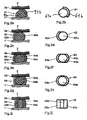
- Fig. 1 shows a schematic diagram of a housing base 1 and a housing cover 2 made of injection-molded plastic for an electronic device (in practice, for example, a mobile phone), both of which are provided with an inside metallization 1a and 2a.
- both housing parts 1 2 screw holes 1b and 2b are formed, wherein the screw holes 1b are formed in the lower housing part for partially self-tapping screwing tapping screws 3 and the screw holes 2b in Dekkel each have a countersink for receiving the screw head of the screws 3. With this screw a need-repeated opening and reclosing of the device housing 4 is possible.
- an arm 5 of a coordinate-controlled handling device (not shown as such) comprises a mandrel 6 having two concentric channels 6a, 6b with hose connections 7a, 7b for supplying two pressurized sealing starting materials 8a, 8b in the direction of the arrow A over the edge portion of the housing base 1 leads.
- a coordinate-controlled handling device (not shown as such) comprises a mandrel 6 having two concentric channels 6a, 6b with hose connections 7a, 7b for supplying two pressurized sealing starting materials 8a, 8b in the direction of the arrow A over the edge portion of the housing base 1 leads.
- the core 9a consists of the first starting material 8a and its surface layer 9b of the second starting material 8b aufdispensiert on the edge portion and adheres firmly there.
- the first starting material 8a is an unfilled air and room temperature curing silicone compound set in a pasty gel state;
- the second starting material 8b is a pasty silicone masterbatch filled with about 50% by weight silvered nickel particles, the matrix of which is substantially the same Composition has like the first material 8a, but in addition in a proportion of less than 1% by mass of a surfactant is mixed as a primer.
- the needle 6 After exiting the needle 6 immediately begins from the surface - without additional technical measures - the curing of the material strand 9 to an elastic, free-form sealing and Ableprofil with a soft core and a highly conductive, but also still relatively elastic, the Core all-round covering surface layer.
- the lid 2 After the curing is substantially complete, - as symbolized by the arrow B - the lid 2 is placed on the lower part 1 and screwed on the screws 3 with this, wherein the sealing and Ableprofil solidified strand 9 without adhering to the lid. 2 is elastically deformed and the gap between the housing parts 1, 2 reliably seals and shields.
- Fig. 2a to 2j are shown in cross-sectional representations different sealing and shielding profiles according to preferred embodiments, together with the order needles used for their preparation.
- the finished profiles are each shown with sections of the adjacent Gezzaueoberfest 1 'and 2, wherein 1' (in contrast to the specification at Fig. 1 ) stands for a metallic lower housing part, while the material for the lid 2 plastic is again selected with a metal coating 2a. (Of course, the invention is also applicable to a full metal housing.)
- the sealing and shielding profile 91 according to Fig. 2a consists of a non-conductive base portion 91a and a conductive layer 91b covering it over slightly more than half of the circumference, and is formed by means of an in Fig. 2b sketched job needle 61 with a first channel 61a with a circular cross-section and this partially surrounding second channel 61b applied with annular segment-shaped cross section on the housing part 1 '.
- the sealing and shielding profile 92 according to Fig. 2c consists of a non-conductive base portion 92a and a conductive edge portion 92b extending over slightly less than half the circumference thereof, and is formed by means of an in Fig. 2d shown applicator needle 62 with a first channel 62a of nikformigem cross-section and a partially surrounding this second channel 62b with approximately nikringsegmentförmigem cross section on the housing part 1 'applied.
- the sealing and shielding profile 93 according to Fig. 2e is different from that Fig. 2c in that on both sides of a non-conductive base part 93a is provided in each case a slightly less than half of the circumference reaching conductive profile part 93b, 93c.
- the profile 93 is determined by means of an in Fig. 2d shown applicator needle 63 with a first channel 63a of circular cross-section and two laterally disposed therefrom channels 63b, 63c generated with approximately nikringsegmentförmigem cross-section.
- a non-conductive core portion 94a is completely covered with a conductive layer 94b, but the thickness thereof is smaller in the gap space adjacent to the housing portions 1 ', 2.
- This profile 94 is determined by means of an in Fig. 2h sketched job needle 64 with a first channel 64a of circular cross section and a second channel 64b surrounding this formed with ellipsoidal cross-section.
- the sealing and shielding profile 95 according to Fig. 2i has a similar (three-component) structure like the one in Fig. 2e However, the material allocation is different: On both sides of a conductive, shielding middle part 95a, a non-conductive, sealing profile part 95b, 95c is provided in each case.
- the profile 95 is determined by means of an in Fig. 2d shown applicator needle 65 is generated with three adjacent channels 65a to 65c with approximately rectangular cross-section.
- the invention is not limited in its execution to the above-mentioned preferred embodiments. Rather, a number of variants is possible, which makes use of the solution shown in other types.
- the specification of the first material is to be understood as "non-conductive" in a broader sense in that this material has significantly lower conductivity (e.g., corresponding to a significantly lower level of metallic filling) than the second material.
- the use of a silicone-based plastic is not mandatory; It can also be used a neoprene or other elastic hardening material, which also does not necessarily have to be room temperature curing.
- the geometry of the profile to be produced and the needle or nozzle cross-sectional shape to be selected depend on the intended use and the specific shape of the shielding housing, and in addition to those in FIG Fig. 2a to 2j sketched variants are many others useful.
Landscapes
- Engineering & Computer Science (AREA)
- Microelectronics & Electronic Packaging (AREA)
- Shielding Devices Or Components To Electric Or Magnetic Fields (AREA)
- Glass Compositions (AREA)
- Cable Accessories (AREA)
- Crystals, And After-Treatments Of Crystals (AREA)
- Mechanical Treatment Of Semiconductor (AREA)
- Coupling Device And Connection With Printed Circuit (AREA)
- Adornments (AREA)
- Pharmaceuticals Containing Other Organic And Inorganic Compounds (AREA)
Claims (15)
- Procédé de fabrication d'un boîtier de blindage (4) le boîtier de blindage (4) comprenant und sous-partie de boîtier (1, 1') et un couvercle de boîtier (2) comme premier respectivement second élément de boîtier, servant de protection mécanique et d'écran électromagnétique à une unité fonctionnelle électronique et comprenant un profil d'étanchéité et de blindage (9 ; 91 à 95) qui remplit un intervalle ménagé entre le premier et le second élément de boîtier contigu (1, 2 ; 1'), constitué d'une masse pâteuse appliquée sous pression directement sur le premier élément de boîtier (1 ; 1') à partir d'un dispositif d'application (5) présentant une aiguille ou une buse (6 ; 61 65) commandé par coordonnées et qui se consolide alors de manière élastique en faisant saillie par adhérence sur celui-ci,
caractérisé en ce que le profil d'étanchéité et de blindage est réalisé par application simultanée au moins d'un premier matériau (8a) ayant des propriétés adaptées à une bonne action d'étanchéité et d'un second matériau (8b) avec des propriétés adaptées à une bonne action de protection en se consolidant également de manière élastique par l'aiguille et/ou la buse munie au moins d'un premier et d'un second canal (6a, 6b ; 61a, 61b ; 62a, 62b ; 63a à 63c ; 64a, 64b ; 65a à 65c), de sorte que le second matériau adhère fermement au premier matériau, et le premier matériau formant un cordon entouré complètement par un cordon du deuxième matériau, le premier canal étant entouré complètement par le second canal en l'aguille et/ou la buse. - Procédé selon la revendication 1, caractérisé en ce que le second élément de boîtier (2) est amené en contact avec le profil d'étanchéité et de blindage (9 ; 91 à 95) après un durcissement essentiellement intégral du premier et/ou du second matériau (8a, 8b).
- Procédé selon la revendication 1 ou 2, caractérisé en ce que le premier matériau (8a) utilisé est pour l'essentiel de la matière synthétique non conductrice, durcissant à l'air et à la température ambiante, et ayant notamment des propriétés thixotropes, en particulier à base de silicone, et le second matériau (8b) mis en oeuvre est pour l'essentiel de la matière synthétique de même nature que le premier matériau, rendue conductrice par des inclusions électriquement conductrices.
- Procédé selon la revendication 3, caractérisé en ce que les inclusions électriquement conductrices utilisées sont des particules, notamment des fibres ou des plaquettes en métal ou en alliage notamment de l'argent ou un alliage argentifère, avec une forte conductibilité électrique.
- Procédé selon la revendication 3, caractérisé en ce que le premier matériau (8a) contient une matière de charge non conductrice, en particulier oxydée ou en céramique.
- Procédé selon l'une des revendications précédentes, caractérisé en ce qu'un agent adhésif est utilisé, qui est en particulier mélangé au matériau, pour l'application du premier et/ou second matériau (8a, 8b).
- Procédé selon la revendication 6, caractérisé en ce que, pour appliquer le profil d'étanchéité et de blindage, on utilise une aiguille ou une buse (6 ; 61 à 64) dont le premier canal (6a ; 61a ; 62a ; 63a ; 64a) essentiellement de section circulaire est entouré de manière concentrique au moins par secteurs par le second canal (6b ; 61b ; 62b ; 63b ; 63c ; 64b), celui-ci ayant pour l'essentiel une section circulaire de forme segmentée.
- Procédé selon l'une des revendications précédentes, caractérisé en ce que le second matériau est appliqué avec une épaisseur irrégulière de section du profil.
- Procédé selon la revendication 8, caractérisé en ce que le second matériau est appliqué sur la face intérieure du boîtier avec une épaisseur plus grande que sur le segment orienté vers un élément de boîtier et/ou sur la face extérieure du boîtier.
- Elément de boîtier d'un boîtier de blindage comprenant une sous-partie de boîtier (1, 1') et un couvercle de boîtier (2) avec un joint appliquée directement sur l'élément de boîtier, le joint étant un joint électriquement conducteur et étant d'un profil d'étanchéité et de protection en forme de cordon, constitué d'un premier matériau et d'un deuxième matériau, le premier matériau étant essentiellement non conducteur avec des propriétés adaptées à une bonne action d'étanchéité, et le deuxième matériau étant un composant ayant des propriétés adaptées à une bonne action de protection par des inclusions électriquement conductrices, le premier matériau formant un cordon entouré complètement par un cordon du deuxième matériau, le profil d'étanchéité et de protection étant appliqué par une aiguille et/ou une buse avec un premier canal étant entouré complètement par un second canal.
- Elément de boîtier selon la revendication 10, caractérisé en ce que les inclusions électriquement conductrices utilisées pour le deuxième composant sont des particules, notamment des fibres ou des plaquettes en métal ou en alliage ayant une conductibilité électrique élevée, notamment de l'argent ou un alliage argentifère.
- Elément de boîtier selon la revendication 10, caractérisé en ce que le premier composant contient une matière de charge non conductrice, en particulier oxydée ou en céramique.
- Elément de boîtier selon l'une des revendications 10 à 12, caractérisé en ce qu'un agent adhésif est mélangé au premier et/ou au deuxième composant.
- Elément de boîtier selon l'une des revendications 10 à 13, caractérisé en ce que le cordon du premier composant est essentiellement de section circulaire et entouré de manière concentrique au moins par secteurs par le cordon du deuxième composant, celui-ci ayant essentiellement une section circulaire segmentée.
- Elément de boîtier selon l'une des revendications 10 à 14, caractérisé en ce que le deuxième composant a une épaisseur irrégulière dans la section du profil.
Priority Applications (2)
| Application Number | Priority Date | Filing Date | Title |
|---|---|---|---|
| EP01105941A EP1111981A1 (fr) | 1997-03-05 | 1998-03-05 | Procédé de fabrication d' un boítier de blindage |
| DE29824567U DE29824567U1 (de) | 1997-03-05 | 1998-03-05 | Elektrisch leitfähige Dichtung |
Applications Claiming Priority (3)
| Application Number | Priority Date | Filing Date | Title |
|---|---|---|---|
| DE19713524 | 1997-03-05 | ||
| DE19713524 | 1997-03-05 | ||
| PCT/DE1998/000682 WO1998039957A1 (fr) | 1997-03-05 | 1998-03-05 | Procede pour fabriquer un boitier de blindage |
Related Child Applications (2)
| Application Number | Title | Priority Date | Filing Date |
|---|---|---|---|
| EP01105941A Division EP1111981A1 (fr) | 1997-03-05 | 1998-03-05 | Procédé de fabrication d' un boítier de blindage |
| EP01105941.7 Division-Into | 2001-03-09 |
Publications (3)
| Publication Number | Publication Date |
|---|---|
| EP0965255A1 EP0965255A1 (fr) | 1999-12-22 |
| EP0965255B1 EP0965255B1 (fr) | 2006-03-01 |
| EP0965255B2 true EP0965255B2 (fr) | 2010-10-20 |
Family
ID=7825178
Family Applications (2)
| Application Number | Title | Priority Date | Filing Date |
|---|---|---|---|
| EP98919059A Expired - Lifetime EP0965255B2 (fr) | 1997-03-05 | 1998-03-05 | Procede pour fabriquer un boitier de blindage |
| EP01105941A Withdrawn EP1111981A1 (fr) | 1997-03-05 | 1998-03-05 | Procédé de fabrication d' un boítier de blindage |
Family Applications After (1)
| Application Number | Title | Priority Date | Filing Date |
|---|---|---|---|
| EP01105941A Withdrawn EP1111981A1 (fr) | 1997-03-05 | 1998-03-05 | Procédé de fabrication d' un boítier de blindage |
Country Status (15)
| Country | Link |
|---|---|
| US (2) | USRE41862E1 (fr) |
| EP (2) | EP0965255B2 (fr) |
| JP (1) | JP2001504280A (fr) |
| KR (1) | KR100362827B1 (fr) |
| CN (1) | CN1143610C (fr) |
| AT (1) | ATE319284T1 (fr) |
| AU (1) | AU732032B2 (fr) |
| CA (1) | CA2283867A1 (fr) |
| DE (3) | DE19880257B4 (fr) |
| DK (1) | DK0965255T3 (fr) |
| HU (1) | HUP0004103A3 (fr) |
| NO (1) | NO323017B1 (fr) |
| RU (1) | RU2192717C2 (fr) |
| TR (1) | TR199902208T2 (fr) |
| WO (1) | WO1998039957A1 (fr) |
Families Citing this family (20)
| Publication number | Priority date | Publication date | Assignee | Title |
|---|---|---|---|---|
| JP3287330B2 (ja) | 1999-04-22 | 2002-06-04 | 日本電気株式会社 | 高周波回路のシールド構造 |
| DE10135038A1 (de) * | 2001-07-18 | 2003-02-06 | Neuhaus Elektronik Gmbh | Elektrisch leitfähige Dichtung |
| US6784363B2 (en) | 2001-10-02 | 2004-08-31 | Parker-Hannifin Corporation | EMI shielding gasket construction |
| US6902639B1 (en) | 2002-01-26 | 2005-06-07 | Reynolds Metals Company | Seaming plastic film using solvent-based adhesive bead |
| GB0328246D0 (en) * | 2003-12-04 | 2004-06-16 | Qinetiq Ltd | Improvements relating to electronic circuit packages |
| JP2008532396A (ja) * | 2005-03-03 | 2008-08-14 | ディアベーテス.オンライン アーゲー | 一体型測定装置を備える携帯電話 |
| US7794147B2 (en) * | 2006-08-25 | 2010-09-14 | Reynolds Packaging Llc | Multiple applications of seaming solutions for heat shrunk bands and labels |
| WO2008033594A1 (fr) * | 2006-09-11 | 2008-03-20 | 3M Innovative Properties Company | Matières conductrices densifiées et articles qui en sont constitués |
| JP5176979B2 (ja) * | 2009-01-22 | 2013-04-03 | セイコーエプソン株式会社 | 弾性表面波装置およびその製造方法 |
| DE102010036919A1 (de) | 2010-08-09 | 2012-02-09 | Aksys Gmbh | Elektrisch leitfähige Dichtung |
| DE102013213233A1 (de) * | 2013-07-05 | 2015-01-08 | Bayerische Motoren Werke Aktiengesellschaft | Verfahren zum Herstellen eines Gehäuses mit einer Schirmung vor elektrischer und/oder magnetischer Strahlung und Gehäuse mit Schirmung vor elektrischer und/oder magnetischer Strahlung |
| US10064317B1 (en) * | 2015-10-27 | 2018-08-28 | Anritsu Company | High isolation shield gasket and method of providing a high isolation shield gasket |
| DE102017123653B4 (de) | 2017-10-11 | 2022-04-28 | Schaeffler Technologies AG & Co. KG | Temperierbares Dichtungselement und Dichtungsanordnung mit diesem |
| CN109759780B (zh) * | 2017-11-10 | 2022-03-22 | 深圳市欢太科技有限公司 | 制备中框的方法、中框及移动终端 |
| WO2020228900A1 (fr) | 2019-05-10 | 2020-11-19 | ATN Hölzel GmbH | Procédé et applicateur pour l'application séquentielle continue d'au moins deux matériaux ou fluides visqueux |
| KR102228724B1 (ko) * | 2019-10-15 | 2021-03-18 | 한국전력공사 | 틈새 매움 부재가 구비된 공가 봉인 밴드 |
| US11017820B1 (en) * | 2020-02-21 | 2021-05-25 | Seagate Technology Llc | Electromagnetic shielding for electronic devices |
| US11276436B1 (en) | 2021-01-05 | 2022-03-15 | Seagate Technology Llc | Corrosive gas reduction for electronic devices |
| DE102023112193A1 (de) | 2023-05-09 | 2024-11-14 | ATN Hölzel GmbH | Applikator und Verfahren zum Betreiben oder Verwenden des erfindungsgemäßen Applikators |
| DE102024207783A1 (de) * | 2024-08-15 | 2026-02-19 | Robert Bosch Gesellschaft mit beschränkter Haftung | Abschirmgehäuse und Verfahren zum Ausbilden eines Abschirmgehäuses |
Citations (2)
| Publication number | Priority date | Publication date | Assignee | Title |
|---|---|---|---|---|
| JPS61149399A (ja) † | 1984-12-25 | 1986-07-08 | Konishiroku Photo Ind Co Ltd | 印刷用原版 |
| DE19733627C1 (de) † | 1997-07-29 | 1998-06-18 | Neuhaus Elektronik Gmbh | Elektrisch leitfähige Dichtung und Verfahren zu deren Herstellung |
Family Cites Families (20)
| Publication number | Priority date | Publication date | Assignee | Title |
|---|---|---|---|---|
| US4098633A (en) | 1977-01-24 | 1978-07-04 | The United States Of America As Represented By The Secretary Of The Navy | Method of making radiation seal |
| JPS60132171A (ja) | 1983-12-19 | 1985-07-15 | Nissan Motor Co Ltd | 液体ガスケツトの塗布方法 |
| GB8616945D0 (en) | 1986-07-11 | 1986-08-20 | Advanced Adhesives Ltd | Simultaneous dispensing of two substances |
| DE8816793U1 (de) | 1988-04-19 | 1990-07-26 | Maibach, Gerd D., 73092 Heiningen | Behälter aus faserverstärktem Kunststoff mit stromleitender Innenschicht |
| JPH0787275B2 (ja) | 1988-10-28 | 1995-09-20 | 北川工業株式会社 | 導電性シール材 |
| US4968854A (en) | 1988-11-10 | 1990-11-06 | Vanguard Products Corporation | Dual elastomer gasket shield for electronic equipment |
| US4945633A (en) * | 1989-03-01 | 1990-08-07 | Nokia-Mobira Oy | Method of mounting a printed circuit board and securing the earthing to a casing |
| US4977295A (en) | 1989-07-28 | 1990-12-11 | Raytheon Company | Gasket impervious to electromagnetic energy |
| US5053924A (en) | 1990-03-30 | 1991-10-01 | Motorola, Inc. | Electromagnetic shield for electrical circuit |
| US5447761A (en) * | 1991-04-19 | 1995-09-05 | Lafond; Luc | Sealant strip incorporating flexing stress alleviating means |
| FI915242L (fi) | 1991-11-06 | 1993-05-07 | Nokia Mobile Phones Ltd | Rf-skaermning av kretskort |
| CA2080177C (fr) | 1992-01-02 | 1997-02-25 | Edward Allan Highum | Blindage electromagnetique; methode de fabrication |
| DE4319965C3 (de) | 1993-06-14 | 2000-09-14 | Emi Tec Elektronische Material | Verfahren zur Herstellung eines Gehäuses mit elektromagnetischer Abschirmung |
| AU672499B2 (en) * | 1993-06-14 | 1996-10-03 | Emi-Tec Elektronische Materialien Gmbh | A process for producing a casing providing a screen against electromagnetic radiation |
| CA2129073C (fr) | 1993-09-10 | 2007-06-05 | John P. Kalinoski | Joints moulants iem |
| DE4340108C3 (de) | 1993-11-22 | 2003-08-14 | Emi Tec Elektronische Material | Abschirmelement und Verfahren zu dessen Herstellung |
| TR199801388T2 (xx) | 1996-01-19 | 1998-10-21 | Tiburtius Bernd | Elektriksel koruma muhafazas�. |
| US6670545B2 (en) | 1999-10-20 | 2003-12-30 | Chemque, Inc. | Conductive coating on a non-conductive flexible substrate |
| WO2001071223A2 (fr) | 2000-03-24 | 2001-09-27 | Chemque, Inc. | Joint, procede et appareil de fabrication dudit joint |
| DE10046557B4 (de) | 2000-09-19 | 2006-07-27 | Datron-Electronic Gmbh | Vorrichtung zum dosierten Ausbringen eines aus mehreren unterschiedlich viskosen Medien bestehenden Materialstranges mittels Koextrusion und mehrfunktionale Kombinationsdichtung |
-
1998
- 1998-03-05 CA CA002283867A patent/CA2283867A1/fr not_active Abandoned
- 1998-03-05 RU RU99121339/09A patent/RU2192717C2/ru active
- 1998-03-05 TR TR1999/02208T patent/TR199902208T2/xx unknown
- 1998-03-05 DK DK98919059T patent/DK0965255T3/da active
- 1998-03-05 DE DE19880257T patent/DE19880257B4/de not_active Expired - Lifetime
- 1998-03-05 AU AU72044/98A patent/AU732032B2/en not_active Expired
- 1998-03-05 AT AT98919059T patent/ATE319284T1/de not_active IP Right Cessation
- 1998-03-05 DE DE29824567U patent/DE29824567U1/de not_active Expired - Lifetime
- 1998-03-05 CN CNB988034727A patent/CN1143610C/zh not_active Expired - Lifetime
- 1998-03-05 EP EP98919059A patent/EP0965255B2/fr not_active Expired - Lifetime
- 1998-03-05 EP EP01105941A patent/EP1111981A1/fr not_active Withdrawn
- 1998-03-05 WO PCT/DE1998/000682 patent/WO1998039957A1/fr not_active Ceased
- 1998-03-05 US US12/111,943 patent/USRE41862E1/en not_active Expired - Lifetime
- 1998-03-05 DE DE59813417T patent/DE59813417D1/de not_active Expired - Lifetime
- 1998-03-05 HU HU0004103A patent/HUP0004103A3/hu unknown
- 1998-03-05 US US09/380,691 patent/US6312550B1/en not_active Ceased
- 1998-03-05 JP JP53807398A patent/JP2001504280A/ja not_active Ceased
- 1998-03-05 KR KR1019997008095A patent/KR100362827B1/ko not_active Expired - Lifetime
-
1999
- 1999-09-03 NO NO19994289A patent/NO323017B1/no not_active IP Right Cessation
Patent Citations (2)
| Publication number | Priority date | Publication date | Assignee | Title |
|---|---|---|---|---|
| JPS61149399A (ja) † | 1984-12-25 | 1986-07-08 | Konishiroku Photo Ind Co Ltd | 印刷用原版 |
| DE19733627C1 (de) † | 1997-07-29 | 1998-06-18 | Neuhaus Elektronik Gmbh | Elektrisch leitfähige Dichtung und Verfahren zu deren Herstellung |
Also Published As
| Publication number | Publication date |
|---|---|
| DE19880257D2 (de) | 1999-09-02 |
| EP1111981A1 (fr) | 2001-06-27 |
| WO1998039957A1 (fr) | 1998-09-11 |
| ATE319284T1 (de) | 2006-03-15 |
| HK1026806A1 (en) | 2000-12-22 |
| DE29824567U1 (de) | 2001-08-16 |
| RU2192717C2 (ru) | 2002-11-10 |
| NO994289L (no) | 1999-11-04 |
| HUP0004103A1 (en) | 2001-03-28 |
| NO323017B1 (no) | 2006-12-27 |
| EP0965255B1 (fr) | 2006-03-01 |
| KR100362827B1 (ko) | 2002-12-11 |
| DE19880257B4 (de) | 2010-12-23 |
| USRE41862E1 (en) | 2010-10-26 |
| EP0965255A1 (fr) | 1999-12-22 |
| NO994289D0 (no) | 1999-09-03 |
| CN1251254A (zh) | 2000-04-19 |
| US6312550B1 (en) | 2001-11-06 |
| AU732032B2 (en) | 2001-04-12 |
| CA2283867A1 (fr) | 1998-09-11 |
| DK0965255T3 (da) | 2006-04-10 |
| TR199902208T2 (xx) | 2000-06-21 |
| AU7204498A (en) | 1998-09-22 |
| HUP0004103A3 (en) | 2002-05-28 |
| JP2001504280A (ja) | 2001-03-27 |
| KR20000076009A (ko) | 2000-12-26 |
| DE59813417D1 (de) | 2006-04-27 |
| CN1143610C (zh) | 2004-03-24 |
Similar Documents
| Publication | Publication Date | Title |
|---|---|---|
| EP0965255B2 (fr) | Procede pour fabriquer un boitier de blindage | |
| EP0875130B1 (fr) | Boitier a effet de blindage electrique | |
| DE4319965C2 (de) | Verfahren zur Herstellung eines Gehäuses | |
| EP0654962B2 (fr) | Membre de blindage et procédé de fabrication d'un tel membre | |
| DE3991286C2 (fr) | ||
| DE60103172T2 (de) | Wellenförmige dichtung mit emi-abschirmung für geringe schliesskräfte | |
| DE69822897T2 (de) | Rohrförmige Dichtung zur verbesserten Abschirmung gegen die Umgebung und elektromagnetische Interferenzen | |
| DE8912397U1 (de) | Leitfähige Dichtung | |
| EP0629114B1 (fr) | Méthode de fabrication d'une boîte blindée contre des ondes électro-magnétiques | |
| EP0895449A2 (fr) | Joint électriquement conducteur ainsi que sa fabrication | |
| EP1055356A1 (fr) | Boitier | |
| EP1034214B1 (fr) | Materiau en matiere plastique et article en matiere plastique conducteur | |
| EP0919115B1 (fr) | Materiau d'etancheite conducteur et joint d'etancheite profile | |
| EP3204462B1 (fr) | Matière d'étanchéité, boîtier et appareil de commande électronique | |
| DE3815517A1 (de) | Dichtung fuer ein elektromagnetische strahlung abschirmendes gehaeuse | |
| EP1345486A2 (fr) | Boítier, respectivement paroi, d' appareil avec joint de blindage revêtu d' un conducteur | |
| DE102008058287B4 (de) | Elektronisches Modul mit einem Dichtelement und Verfahren zum Herstellen des Moduls | |
| DE102021129840A1 (de) | Elektrischer Leiter für die Leitung elektrischen Stroms durch ein Gehäuse und Verfahren zur Herstellung | |
| DE4345594B4 (de) | Verfahren zur Herstellung eines eine Abschirmung gegen elektromagnetische Abstrahlung aufweisenden Gehäuses | |
| EP2257993A1 (fr) | Module solaire et procédé de fabrication associé | |
| DE19858111C2 (de) | Abgedichteter Steckverbinder und Verfahren zu dessen Herstellung | |
| DE4345582B4 (de) | Gehäuse, das seinen Innenraum gegen elektromagnetische Strahlung abschirmt | |
| DE10060917A1 (de) | Abschirmung gegen elektromagnetische Strahlung | |
| DE102024108740A1 (de) | Wellenerdungsring | |
| DE2919540A1 (de) | Abgedichtetes gehaeuse aus metall und kunststoff fuer halbleiter-vorrichtungen |
Legal Events
| Date | Code | Title | Description |
|---|---|---|---|
| PUAI | Public reference made under article 153(3) epc to a published international application that has entered the european phase |
Free format text: ORIGINAL CODE: 0009012 |
|
| 17P | Request for examination filed |
Effective date: 19990903 |
|
| AK | Designated contracting states |
Kind code of ref document: A1 Designated state(s): AT BE CH DE DK ES FI FR GB IE IT LI NL PT SE |
|
| GRAG | Despatch of communication of intention to grant |
Free format text: ORIGINAL CODE: EPIDOS AGRA |
|
| 17Q | First examination report despatched |
Effective date: 20001205 |
|
| GRAG | Despatch of communication of intention to grant |
Free format text: ORIGINAL CODE: EPIDOS AGRA |
|
| GRAG | Despatch of communication of intention to grant |
Free format text: ORIGINAL CODE: EPIDOS AGRA |
|
| GRAH | Despatch of communication of intention to grant a patent |
Free format text: ORIGINAL CODE: EPIDOS IGRA |
|
| GRAH | Despatch of communication of intention to grant a patent |
Free format text: ORIGINAL CODE: EPIDOS IGRA |
|
| GRAN | Information related to approval following communication of intention to grant deleted |
Free format text: ORIGINAL CODE: EPIDOSDAGR4 |
|
| GRAJ | Information related to disapproval of communication of intention to grant by the applicant or resumption of examination proceedings by the epo deleted |
Free format text: ORIGINAL CODE: EPIDOSDIGR1 |
|
| GRAL | Information related to payment of fee for publishing/printing deleted |
Free format text: ORIGINAL CODE: EPIDOSDIGR3 |
|
| GRAP | Despatch of communication of intention to grant a patent |
Free format text: ORIGINAL CODE: EPIDOSNIGR1 |
|
| GRAS | Grant fee paid |
Free format text: ORIGINAL CODE: EPIDOSNIGR3 |
|
| GRAA | (expected) grant |
Free format text: ORIGINAL CODE: 0009210 |
|
| AK | Designated contracting states |
Kind code of ref document: B1 Designated state(s): AT BE CH DE DK ES FI FR GB IE IT LI NL PT SE |
|
| PG25 | Lapsed in a contracting state [announced via postgrant information from national office to epo] |
Ref country code: NL Free format text: LAPSE BECAUSE OF FAILURE TO SUBMIT A TRANSLATION OF THE DESCRIPTION OR TO PAY THE FEE WITHIN THE PRESCRIBED TIME-LIMIT Effective date: 20060301 Ref country code: IT Free format text: LAPSE BECAUSE OF FAILURE TO SUBMIT A TRANSLATION OF THE DESCRIPTION OR TO PAY THE FEE WITHIN THE PRESCRIBED TIME-LIMIT;WARNING: LAPSES OF ITALIAN PATENTS WITH EFFECTIVE DATE BEFORE 2007 MAY HAVE OCCURRED AT ANY TIME BEFORE 2007. THE CORRECT EFFECTIVE DATE MAY BE DIFFERENT FROM THE ONE RECORDED. Effective date: 20060301 Ref country code: IE Free format text: LAPSE BECAUSE OF FAILURE TO SUBMIT A TRANSLATION OF THE DESCRIPTION OR TO PAY THE FEE WITHIN THE PRESCRIBED TIME-LIMIT Effective date: 20060301 |
|
| REG | Reference to a national code |
Ref country code: GB Ref legal event code: FG4D Free format text: NOT ENGLISH |
|
| REG | Reference to a national code |
Ref country code: CH Ref legal event code: EP |
|
| PG25 | Lapsed in a contracting state [announced via postgrant information from national office to epo] |
Ref country code: BE Free format text: LAPSE BECAUSE OF NON-PAYMENT OF DUE FEES Effective date: 20060331 |
|
| REG | Reference to a national code |
Ref country code: IE Ref legal event code: FG4D Free format text: LANGUAGE OF EP DOCUMENT: GERMAN |
|
| REG | Reference to a national code |
Ref country code: DK Ref legal event code: T3 |
|
| REF | Corresponds to: |
Ref document number: 59813417 Country of ref document: DE Date of ref document: 20060427 Kind code of ref document: P |
|
| PG25 | Lapsed in a contracting state [announced via postgrant information from national office to epo] |
Ref country code: ES Free format text: LAPSE BECAUSE OF FAILURE TO SUBMIT A TRANSLATION OF THE DESCRIPTION OR TO PAY THE FEE WITHIN THE PRESCRIBED TIME-LIMIT Effective date: 20060612 |
|
| REG | Reference to a national code |
Ref country code: SE Ref legal event code: TRGR |
|
| GBT | Gb: translation of ep patent filed (gb section 77(6)(a)/1977) |
Effective date: 20060530 |
|
| PG25 | Lapsed in a contracting state [announced via postgrant information from national office to epo] |
Ref country code: DK Free format text: LAPSE BECAUSE OF NON-PAYMENT OF DUE FEES Effective date: 20060630 |
|
| PG25 | Lapsed in a contracting state [announced via postgrant information from national office to epo] |
Ref country code: PT Free format text: LAPSE BECAUSE OF FAILURE TO SUBMIT A TRANSLATION OF THE DESCRIPTION OR TO PAY THE FEE WITHIN THE PRESCRIBED TIME-LIMIT Effective date: 20060801 |
|
| NLV1 | Nl: lapsed or annulled due to failure to fulfill the requirements of art. 29p and 29m of the patents act | ||
| REG | Reference to a national code |
Ref country code: HK Ref legal event code: GR Ref document number: 1026806 Country of ref document: HK |
|
| REG | Reference to a national code |
Ref country code: IE Ref legal event code: FD4D |
|
| ET | Fr: translation filed | ||
| PLBI | Opposition filed |
Free format text: ORIGINAL CODE: 0009260 |
|
| PLAX | Notice of opposition and request to file observation + time limit sent |
Free format text: ORIGINAL CODE: EPIDOSNOBS2 |
|
| 26 | Opposition filed |
Opponent name: LAIRD TECHNOLOGIES Effective date: 20061201 |
|
| REG | Reference to a national code |
Ref country code: DK Ref legal event code: EBP |
|
| PLBB | Reply of patent proprietor to notice(s) of opposition received |
Free format text: ORIGINAL CODE: EPIDOSNOBS3 |
|
| BERE | Be: lapsed |
Owner name: KAHL, HELMUT Effective date: 20060331 Owner name: TIBURTIUS, BERND Effective date: 20060331 |
|
| PGFP | Annual fee paid to national office [announced via postgrant information from national office to epo] |
Ref country code: AT Payment date: 20090323 Year of fee payment: 12 |
|
| PGFP | Annual fee paid to national office [announced via postgrant information from national office to epo] |
Ref country code: CH Payment date: 20090325 Year of fee payment: 12 |
|
| PGFP | Annual fee paid to national office [announced via postgrant information from national office to epo] |
Ref country code: SE Payment date: 20090325 Year of fee payment: 12 |
|
| PUAH | Patent maintained in amended form |
Free format text: ORIGINAL CODE: 0009272 |
|
| STAA | Information on the status of an ep patent application or granted ep patent |
Free format text: STATUS: PATENT MAINTAINED AS AMENDED |
|
| 27A | Patent maintained in amended form |
Effective date: 20101020 |
|
| AK | Designated contracting states |
Kind code of ref document: B2 Designated state(s): AT BE CH DE DK ES FI FR GB IE IT LI NL PT SE |
|
| REG | Reference to a national code |
Ref country code: CH Ref legal event code: PL Ref country code: CH Ref legal event code: AEN Free format text: AUFRECHTERHALTUNG DES PATENTES IN GEAENDERTER FORM |
|
| EUG | Se: european patent has lapsed | ||
| PG25 | Lapsed in a contracting state [announced via postgrant information from national office to epo] |
Ref country code: AT Free format text: LAPSE BECAUSE OF NON-PAYMENT OF DUE FEES Effective date: 20100305 |
|
| PG25 | Lapsed in a contracting state [announced via postgrant information from national office to epo] |
Ref country code: LI Free format text: LAPSE BECAUSE OF NON-PAYMENT OF DUE FEES Effective date: 20100331 Ref country code: CH Free format text: LAPSE BECAUSE OF NON-PAYMENT OF DUE FEES Effective date: 20100331 |
|
| REG | Reference to a national code |
Ref country code: ES Ref legal event code: FD2A Effective date: 20110419 |
|
| PG25 | Lapsed in a contracting state [announced via postgrant information from national office to epo] |
Ref country code: ES Free format text: LAPSE BECAUSE OF FAILURE TO SUBMIT A TRANSLATION OF THE DESCRIPTION OR TO PAY THE FEE WITHIN THE PRESCRIBED TIME-LIMIT Effective date: 20100306 |
|
| PG25 | Lapsed in a contracting state [announced via postgrant information from national office to epo] |
Ref country code: SE Free format text: LAPSE BECAUSE OF NON-PAYMENT OF DUE FEES Effective date: 20100306 |
|
| REG | Reference to a national code |
Ref country code: FR Ref legal event code: PLFP Year of fee payment: 19 |
|
| REG | Reference to a national code |
Ref country code: FR Ref legal event code: PLFP Year of fee payment: 20 |
|
| PGFP | Annual fee paid to national office [announced via postgrant information from national office to epo] |
Ref country code: FI Payment date: 20170322 Year of fee payment: 20 Ref country code: FR Payment date: 20170323 Year of fee payment: 20 |
|
| PGFP | Annual fee paid to national office [announced via postgrant information from national office to epo] |
Ref country code: GB Payment date: 20170327 Year of fee payment: 20 |
|
| PGFP | Annual fee paid to national office [announced via postgrant information from national office to epo] |
Ref country code: DE Payment date: 20170525 Year of fee payment: 20 |
|
| REG | Reference to a national code |
Ref country code: DE Ref legal event code: R071 Ref document number: 59813417 Country of ref document: DE |
|
| REG | Reference to a national code |
Ref country code: GB Ref legal event code: PE20 Expiry date: 20180304 |
|
| PG25 | Lapsed in a contracting state [announced via postgrant information from national office to epo] |
Ref country code: GB Free format text: LAPSE BECAUSE OF EXPIRATION OF PROTECTION Effective date: 20180304 |