EP0966036A2 - Herstellungsverfahren für ein Halbleiterbauelement mit verschiedenen Gateoxidschichten - Google Patents
Herstellungsverfahren für ein Halbleiterbauelement mit verschiedenen Gateoxidschichten Download PDFInfo
- Publication number
- EP0966036A2 EP0966036A2 EP99304134A EP99304134A EP0966036A2 EP 0966036 A2 EP0966036 A2 EP 0966036A2 EP 99304134 A EP99304134 A EP 99304134A EP 99304134 A EP99304134 A EP 99304134A EP 0966036 A2 EP0966036 A2 EP 0966036A2
- Authority
- EP
- European Patent Office
- Prior art keywords
- gate
- active
- width
- oxide layer
- gate pattern
- Prior art date
- Legal status (The legal status is an assumption and is not a legal conclusion. Google has not performed a legal analysis and makes no representation as to the accuracy of the status listed.)
- Granted
Links
Images


Classifications
-
- H—ELECTRICITY
- H10—SEMICONDUCTOR DEVICES; ELECTRIC SOLID-STATE DEVICES NOT OTHERWISE PROVIDED FOR
- H10B—ELECTRONIC MEMORY DEVICES
- H10B12/00—Dynamic random access memory [DRAM] devices
- H10B12/01—Manufacture or treatment
-
- H—ELECTRICITY
- H10—SEMICONDUCTOR DEVICES; ELECTRIC SOLID-STATE DEVICES NOT OTHERWISE PROVIDED FOR
- H10D—INORGANIC ELECTRIC SEMICONDUCTOR DEVICES
- H10D84/00—Integrated devices formed in or on semiconductor substrates that comprise only semiconducting layers, e.g. on Si wafers or on GaAs-on-Si wafers
- H10D84/01—Manufacture or treatment
- H10D84/0123—Integrating together multiple components covered by H10D12/00 or H10D30/00, e.g. integrating multiple IGBTs
- H10D84/0126—Integrating together multiple components covered by H10D12/00 or H10D30/00, e.g. integrating multiple IGBTs the components including insulated gates, e.g. IGFETs
- H10D84/0144—Manufacturing their gate insulating layers
-
- H—ELECTRICITY
- H10—SEMICONDUCTOR DEVICES; ELECTRIC SOLID-STATE DEVICES NOT OTHERWISE PROVIDED FOR
- H10D—INORGANIC ELECTRIC SEMICONDUCTOR DEVICES
- H10D84/00—Integrated devices formed in or on semiconductor substrates that comprise only semiconducting layers, e.g. on Si wafers or on GaAs-on-Si wafers
- H10D84/01—Manufacture or treatment
- H10D84/02—Manufacture or treatment characterised by using material-based technologies
- H10D84/03—Manufacture or treatment characterised by using material-based technologies using Group IV technology, e.g. silicon technology or silicon-carbide [SiC] technology
- H10D84/038—Manufacture or treatment characterised by using material-based technologies using Group IV technology, e.g. silicon technology or silicon-carbide [SiC] technology using silicon technology, e.g. SiGe
Definitions
- the present invention relates to a semiconductor device manufacturing method, and more particularly to a method for forming different gate oxide layers in a single chip.
- Fig.1 schematically shows the relationship between electrical field(MV/cm) and gate oxide thickness( ⁇ ) with respect to high voltage logic device and normal voltage logic device.
- V DD supply voltage
- the transistor characteristics can be increased by reducing gate oxide thickness while keeping the supply voltage at a constant level.
- the power consumption can be reduced by decreasing the supply voltage while keeping the gate oxide thickness at a constant level. Therefore, it is required that the gate oxide thickness be reduced without breakdown thereof while keeping a constant electric field which is so called "constant electric field scaling law".
- Another approach is to fabricate the cell array region and peripheral region on different chips, not on a single chip. This method, however, has a disadvantage of requiring process complexity and is not compatible with low-cost fabrication.
- the present invention was made in view of the above problem, and it is therefore an object of the invention to provide a method for forming different gate oxide layers in a single chip and more particularly a method for forming different gate oxide layers after formation of the gate electrode.
- a key feature of this invention is to form different gate oxide layers through the oxidation process which is dependent on dimension of the active width. The active width dependent oxidation process is carried out after formation of the complete transistor(formation of the sidewall spacers).
- Different dimension of the active areas are defined in and on the semiconductor substrate.
- a first thin gate oxide layer is formed on the overall active areas with a same thickness.
- Different gate patterns are formed over the thin oxide layer of the active areas. The gate patterns are crossing the active areas in parallel with width direction.
- gate patterns are formed to have narrow distance between adjacent gate pattern while wide distance between adjacent gate patterns in the wide region(peripheral region).
- Gate spacers are formed on lateral edges of the patterned gates.
- Critical wet oxidation is carried out and thereby growing the thin oxide layer in the narrow active region(cell array region). The wet oxidation allows gate oxide growth to a greater extend in the narrow active region than wide active region(peripheral region).
- different gate oxide layers are formed in one chip, i.e., thick gate oxide layer in the cell array region and relatively thin gate oxide layer in the peripheral region.
- the active width is narrow(in the cell array region)
- the oxidant from the gate width direction i.e., from the field oxide
- the active width is wide(in the peripheral region)
- amount of the oxidant from the gate width direction is small considering the active size, so that the thickness variation of the thin gate oxide layer is negligible. Accordingly, different gate oxide layers are formed in one chip.
- the present invention relates to a method for forming different gate oxide layers in a single chip using active dimension dependent oxygen diffusivity.
- the effective gate oxide layer is completely formed after completely forming the gate pattern.
- Fig.2 shows the relationship between degree of cell density and cell efficiency thereof.
- the degree of cell density is proportional to cell efficiency.
- the cell efficiency increases, too. That is because cell density increase in the cell array region while same circuit is used in the peripheral region.
- gate oxide reliability arises easily in the cell array region due to larger electrical field than in the peripheral region. Therefore, it is needed a device that has a different gate oxide layers, i.e., thicker gate oxide in the cell array region and thin gate oxide layer in the peripheral region.
- the present invention provides a high voltage device and a normal voltage device by more than 30% threshold voltage difference therebetween on a single chip.
- the high voltage device has a thicker gate oxide and the normal voltage device has a relatively thin gate oxide.
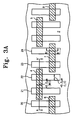
- Figs.3A and 3B illustrate top plan views of a semiconductor substrate where a plurality of gate patterns are formed intersecting active area surrounded by a filed oxide layer, respectively cell array region and peripheral region.
- the gate patterns 20-24 intersects the active areas 4-8.
- active width is indicated by reference number "W1” and gate length is indicated by reference number “L1".
- active width("W1") in the cell array region is 0.2 micrometers or less and gate length("L1") is 0.2 micrometers or less.
- Reference number 2 represents the field oxide layer which surrounds the active areas 4-8.
- active areas 9 and 10 are surrounded by the filed oxide layer 2.
- the active areas 9 and 10 of the peripheral region has a wider active width( "W2") than that of the cell array region in Fig.3A.
- a plurality of gate patters 26-30 are formed running parallel with the active width direction.
- only one gate pattern are intersecting one active area.
- the gate pattern 27 are intersecting the active area 9 and the gate pattern 29 are intersecting the active area 10.
- More than 90% of the active width("W2") of the peripheral region is at least two times as large as the cell array region(0.2 micrometers) and most of the active areas are 1.0 micrometers active width.
- the gate length of the gate patterns of the peripheral region is about 0.2 micrometers to 3.0 micrometers, and most of them are about 0.2 micrometers to 1.0 micrometers.
- the gate pattern 27 has a gate length("L2") of about 0.2 micrometers and the gate pattern 29 has a gate length( "L3") of about 1.0 micrometers or more.
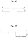
- Figs.4A to 4B are cross-sectional views, respectively taken along line A-A' and line B-B' of Figs.3A before the formation of the gate pattern.
- Figs.4C to 4D are cross-sectional views, respectively taken along line C-C' and line D-D' of Figs.3B before the formation of the gate pattern.
- the field oxide layer 2 is formed to define active areas 4 and 7(cell array region, or high voltage region) and 9 and 10(peripheral region, or normal voltage region) on the semiconductor substrate (not shown).
- the active width("W1", 7) of the cell array region(see Fig.4B) is formed to be narrower than the active width("W2", 9) of the peripheral region(see Fig.4C).
- the active width("W1") of the cell array region is about 0.2 micrometers or less and the active width("W2") of the peripheral region is about 0.4 micrometers or more.
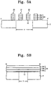
- Figs.5A to 5D respectively illustrate a process step subsequent to that shown in Figs.4A to 4D wherein gate pattern is formed.
- conventional ion implanting process such as well ion implantation, field ion implantation, and channel ion implantation are carried out.
- first gate oxide layer 12 is formed over the entire semiconductor surface. The thickness of the first gate oxide is not affected by the active areas dimension. The gate oxide layer 12 is uniformly throughout the semiconductor surface. Stacked gate electrode patterns 20-24(cell array region) and 27 and 29(peripheral region) are formed.
- the gate patterns are formed by the process sequence of depositing doped polysilicon layers 23a, 24a, 27a, and 29a, suicide layers 23b, 24b, 27b, and 29b such as WSi x , TiSi x , and MoSi x , hard mask layers 23c, 24c, 27c, and 29c such as Si 3 N 4 , HTO(high temperature oxide), PE-CVD(plasma enhanced chemical vapor deposition) oxide, and anti-reflection layer and then patterning to desired configuration by photo-etching process.
- the hard mask serves as etching mask and ion implanting mask.
- the gate patterns 20-24 of the cell array region have a gate length("L1") of about 0.2 microns or less.
- the gate patterns 27 and 29 of the peripheral region have a gate length of one and a half times as large as the cell array region, for example 0.2 micrometers to 3.0 micrometers, preferably most of them are 0.2 micrometers to 1.0 micrometers.
- This anisotropic dry etching for gate patterning causes substrate damages and gate oxide encroachment at the bottom edges of the gate pattern.
- gate poly oxidation process is carried out to form a second oxide layer(not shown) on the lateral edges of the gate patterns and on the surface of the semiconductor substrate outside of the gate patterns.
- bird's beak phenomenon is occurred in the bottom edges of the gate pattern so that the second oxide layer grows thickly. Electrical field are concentrated at the bottom edges of the gate patterns due to thicker oxide layer and thereby preventing degradation of the gate oxide.
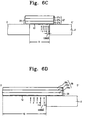
- Figs.6A to 6D respectively illustrate a process step subsequent to that shown in Figs.5A to 5D wherein gate spacers are formed and then oxidation is carried out.
- oxide spacers 30 are formed conventionally on the first oxide layer on lateral edges of the gate patterns 20-24,27 and 29. This oxide spacers 30 serve dual purpose of oxidation barrier layer in the subsequent wet oxidation and self aligned mask for ion implantation.
- critical wet oxidation is carried out to form a third oxide layer(not shown) at a temperature of about 750°C to 850°C. Due to this wet oxidation, effective gate oxide thickness grows differently dependent on the active dimension(active width) and thereby forming different gate oxide layers in a single chip.
- Oxide layer grows thickly in the cell array region while grows very thin in the peripheral region. This is because, during this wet oxidation, oxidant diffusivity from thick field oxide layer(active width direction) greatly affects the oxidation process while the oxidant diffusivity from gate oxide layer(gate length direction) is negligible in both cell array region and peripheral region. In other words, the oxidants from the gate length direction greatly affect the oxidation in the cell region with small active areas while affect nearly the oxidation in the peripheral region with large active areas. Accordingly, oxide layer in the cell array region grows thickly in both active width and gate length directions due to its narrow active width. On the other hand, oxide layer grows very thin in the peripheral areas due to its wide active width. Therefore, different gate oxide layers are formed in single chip.
- Figs.6A to 6D there are provided five arrows(serial numbers 1 to 5) pointing out certain point of gate oxide layer.
- the thickness of the gate oxide layer pointed by the arrows 1 to 5 is 107 ⁇ , 103 ⁇ , 100 ⁇ , 103 ⁇ , and 107 ⁇ , respectively.
- the thickness of the gate oxide layer pointed by the arrows 1 to 5 is 110 ⁇ , 105 ⁇ , 100 ⁇ , 105 ⁇ , and 110 ⁇ , respectively.
- the distance between each arrow and the next is 100 ⁇ .
- Resulting gate oxide layer in the cell array region shown in Figs.6A and 6B is grown thickly as compared to before wet oxidation.
- the thickness of the gate oxide layer pointed by the arrows 1 to 5 is 67 ⁇ , 67 ⁇ , 67 ⁇ , 75 ⁇ , and 107 ⁇ , respectively.
- the thickness of the gate oxide layer pointed by the arrows 1 to 5 is 60 ⁇ , 60 ⁇ , 60 ⁇ , 60 ⁇ , and 77 ⁇ , respectively.
- the distance between each arrow and the next is 1000 ⁇ and 5000 ⁇ , respectively.
- oxide layer grows thickly at bottom edges of the gate electrode and oxide layer except at the bottom edges is substantially same thickness as oxide layer before wet oxidation.
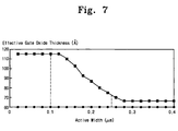
- Fig.7 shows the relationship between the thickness variation of the effective gate oxide and the active width under fixed gate pattern size(0.2 micrometers) by using the T-SUPREM4 and MEDICI(procell & device simulator).
- This simulation method was carried out under the condition that the gate pattern size is fixed at 0.2 micrometers and the wet oxidation is carried out on the bare wafer having 60 ⁇ oxide layer at a temperature about 780°C for 25minutes in 10 liters H 2 O atmosphere.
- the thickness variation is about 7 ⁇ due to small gate pattern size. If the active width is in the range between 0.25 micrometers and 0.1 micrometers, the oxide thickness significantly increases due to bird's beak phenomenon. If the active width is less than 0.1 micrometers, bird's beak phenomenon becomes severe to cause bird's beak punchthrough(oxidant punchthrough) phenomenon. The thickness of the oxide layer increase from initial 60 ⁇ to 115 ⁇ . This bird's beak punchthrough(oxidant punchthrough) region can be adjusted(i.e., can be shifted to a desired region) dependent on the wet oxidation condition.
- ⁇ x ⁇ (1/a 2 -1/b 2 )
- ⁇ oxide viscosity
- ⁇ velocity constant determined by oxide growth rate at the interface
- a and b radius of coverture of oxide layer measuring respectively at upper surface and lower surface(facing the silicon substrate).
- D D* 0 exp(-P*V 0 /kT) wherein P is bulk oxide stress
- this invention performs wet oxidation after formation of the insulating spacers so as to intensify the influence of the active width on oxide growth during oxidation.
- the insulating spacers serves to path of oxidation blocking.
- wet oxidation is preferably selected as oxidation ambient because wet oxidation has high solubility(more than 600 times as high as dry oxidation) and water(H 2 O) reacts with SiO to form hydroxyl group which breakdowns the SiO 2 and thereby reduces viscosity thereof. This reduces above mentioned bulk oxide stress and thereby increasing oxidation rate.
Landscapes
- Engineering & Computer Science (AREA)
- Manufacturing & Machinery (AREA)
- Metal-Oxide And Bipolar Metal-Oxide Semiconductor Integrated Circuits (AREA)
- Semiconductor Memories (AREA)
Applications Claiming Priority (2)
| Application Number | Priority Date | Filing Date | Title |
|---|---|---|---|
| KR9822434 | 1998-06-15 | ||
| KR1019980022434A KR100267010B1 (ko) | 1998-06-15 | 1998-06-15 | 반도체 장치의 제조 방법 |
Publications (3)
| Publication Number | Publication Date |
|---|---|
| EP0966036A2 true EP0966036A2 (de) | 1999-12-22 |
| EP0966036A3 EP0966036A3 (de) | 2000-10-18 |
| EP0966036B1 EP0966036B1 (de) | 2008-11-26 |
Family
ID=19539577
Family Applications (1)
| Application Number | Title | Priority Date | Filing Date |
|---|---|---|---|
| EP99304134A Expired - Lifetime EP0966036B1 (de) | 1998-06-15 | 1999-05-27 | Herstellungsverfahren für ein Halbleiterbauelement mit verschiedenen Gateoxidschichten |
Country Status (7)
| Country | Link |
|---|---|
| US (1) | US6329249B1 (de) |
| EP (1) | EP0966036B1 (de) |
| JP (1) | JP4271779B2 (de) |
| KR (1) | KR100267010B1 (de) |
| CN (1) | CN1227719C (de) |
| DE (1) | DE69939963D1 (de) |
| TW (1) | TW444295B (de) |
Cited By (1)
| Publication number | Priority date | Publication date | Assignee | Title |
|---|---|---|---|---|
| US6645817B2 (en) | 2001-07-03 | 2003-11-11 | Koninklijke Philips Electronics N.V. | Method of manufacturing a semiconductor device comprising MOS-transistors having gate oxides of different thicknesses |
Families Citing this family (2)
| Publication number | Priority date | Publication date | Assignee | Title |
|---|---|---|---|---|
| KR101181050B1 (ko) | 2011-01-31 | 2012-09-10 | 주식회사 동부하이텍 | 전원 관리 소자 |
| KR102458453B1 (ko) | 2020-12-15 | 2022-10-27 | 대한민국 | 석발기가 구비된 곡물 정선장치 |
Family Cites Families (13)
| Publication number | Priority date | Publication date | Assignee | Title |
|---|---|---|---|---|
| US4352236A (en) * | 1981-07-24 | 1982-10-05 | Intel Corporation | Double field oxidation process |
| US5371026A (en) * | 1992-11-30 | 1994-12-06 | Motorola Inc. | Method for fabricating paired MOS transistors having a current-gain differential |
| US5756385A (en) * | 1994-03-30 | 1998-05-26 | Sandisk Corporation | Dense flash EEPROM cell array and peripheral supporting circuits formed in deposited field oxide with the use of spacers |
| JP3532625B2 (ja) * | 1994-10-06 | 2004-05-31 | 東芝マイクロエレクトロニクス株式会社 | 半導体装置の製造方法 |
| US5595922A (en) * | 1994-10-28 | 1997-01-21 | Texas Instruments | Process for thickening selective gate oxide regions |
| JP3444687B2 (ja) * | 1995-03-13 | 2003-09-08 | 三菱電機株式会社 | 不揮発性半導体記憶装置 |
| DE69630864T2 (de) * | 1996-01-31 | 2004-11-04 | Sgs-Thomson Microelectronics S.R.L., Agrate Brianza | Verfahren zur Herstellung nichtflüchtiger Speicheranordnungen mit Tunneloxid |
| KR100224780B1 (ko) * | 1996-12-31 | 1999-10-15 | 김영환 | 반도체 소자의 필드산화막 제조방법 |
| TW327701B (en) * | 1997-07-21 | 1998-03-01 | United Semiconductor Corp | The flash memory cell |
| KR100268409B1 (ko) * | 1998-05-20 | 2000-10-16 | 윤종용 | 반도체 장치의 제조 방법 |
| US6046086A (en) * | 1998-06-19 | 2000-04-04 | Taiwan Semiconductor Manufacturing Company | Method to improve the capacity of data retention and increase the coupling ratio of source to floating gate in split-gate flash |
| US5960289A (en) * | 1998-06-22 | 1999-09-28 | Motorola, Inc. | Method for making a dual-thickness gate oxide layer using a nitride/oxide composite region |
| US6204159B1 (en) * | 1999-07-09 | 2001-03-20 | Advanced Micro Devices, Inc. | Method of forming select gate to improve reliability and performance for NAND type flash memory devices |
-
1998
- 1998-06-15 KR KR1019980022434A patent/KR100267010B1/ko not_active Expired - Fee Related
-
1999
- 1999-04-15 TW TW088105998A patent/TW444295B/zh not_active IP Right Cessation
- 1999-05-27 DE DE69939963T patent/DE69939963D1/de not_active Expired - Lifetime
- 1999-05-27 EP EP99304134A patent/EP0966036B1/de not_active Expired - Lifetime
- 1999-06-15 JP JP16897599A patent/JP4271779B2/ja not_active Expired - Fee Related
- 1999-06-15 US US09/333,574 patent/US6329249B1/en not_active Expired - Lifetime
- 1999-06-15 CN CNB991090519A patent/CN1227719C/zh not_active Expired - Fee Related
Cited By (2)
| Publication number | Priority date | Publication date | Assignee | Title |
|---|---|---|---|---|
| US6645817B2 (en) | 2001-07-03 | 2003-11-11 | Koninklijke Philips Electronics N.V. | Method of manufacturing a semiconductor device comprising MOS-transistors having gate oxides of different thicknesses |
| WO2003005439A3 (en) * | 2001-07-03 | 2004-05-21 | Koninkl Philips Electronics Nv | Method of manufacturing a semiconductor device comprising mos-transistors having gate oxides of different thicknesses |
Also Published As
| Publication number | Publication date |
|---|---|
| KR20000001947A (ko) | 2000-01-15 |
| JP4271779B2 (ja) | 2009-06-03 |
| US6329249B1 (en) | 2001-12-11 |
| EP0966036B1 (de) | 2008-11-26 |
| EP0966036A3 (de) | 2000-10-18 |
| TW444295B (en) | 2001-07-01 |
| JP2000031423A (ja) | 2000-01-28 |
| DE69939963D1 (de) | 2009-01-08 |
| CN1239819A (zh) | 1999-12-29 |
| KR100267010B1 (ko) | 2000-09-15 |
| CN1227719C (zh) | 2005-11-16 |
Similar Documents
| Publication | Publication Date | Title |
|---|---|---|
| US5742095A (en) | Method of fabricating planar regions in an integrated circuit | |
| US5696019A (en) | Self-aligned trench isolation for memory array using sidewall spacers | |
| US4532696A (en) | Method of manufacturing a semiconductor device for forming a deep field region in a semiconductor substrate | |
| EP0685883B1 (de) | Verfahren zur Herstellung einer verbesserten dielektrischen Schicht für eine integrierte Schaltung | |
| US6136657A (en) | Method for fabricating a semiconductor device having different gate oxide layers | |
| US5811865A (en) | Dielectric in an integrated circuit | |
| JP4551795B2 (ja) | 半導体装置の製造方法 | |
| US6818505B2 (en) | Non-volatile semiconductor memory device and manufacturing method thereof | |
| US6207515B1 (en) | Method of fabricating buried source to shrink chip size in memory array | |
| EP0966036B1 (de) | Herstellungsverfahren für ein Halbleiterbauelement mit verschiedenen Gateoxidschichten | |
| US5972749A (en) | Method for preventing P1 punchthrough | |
| US6855993B2 (en) | Semiconductor devices and methods for fabricating the same | |
| JPS643070B2 (de) | ||
| JP3850104B2 (ja) | 半導体装置の製造方法 | |
| KR100262017B1 (ko) | 셀 제조방법 | |
| US5952720A (en) | Buried contact structure | |
| KR20000044855A (ko) | 플래쉬 메모리 소자의 제조 방법 | |
| JPH03257873A (ja) | 不揮発性半導体記憶装置及びその製造方法 | |
| KR19990029710A (ko) | 반도체 디바이스 및 그 제조 방법 | |
| JPS5943832B2 (ja) | 半導体装置の製造方法 | |
| JPH10189952A (ja) | 半導体装置およびその製造方法 | |
| JPH10189710A (ja) | 半導体装置およびその製造方法 | |
| JPS60251641A (ja) | 半導体装置およびその製造方法 | |
| JPH07226501A (ja) | Mosトランジスタの製造方法 | |
| JPH04186777A (ja) | 半導体装置の製造方法 |
Legal Events
| Date | Code | Title | Description |
|---|---|---|---|
| PUAI | Public reference made under article 153(3) epc to a published international application that has entered the european phase |
Free format text: ORIGINAL CODE: 0009012 |
|
| 17P | Request for examination filed |
Effective date: 19990623 |
|
| AK | Designated contracting states |
Kind code of ref document: A2 Designated state(s): DE FR GB NL |
|
| AX | Request for extension of the european patent |
Free format text: AL;LT;LV;MK;RO;SI |
|
| PUAL | Search report despatched |
Free format text: ORIGINAL CODE: 0009013 |
|
| AK | Designated contracting states |
Kind code of ref document: A3 Designated state(s): AT BE CH CY DE DK ES FI FR GB GR IE IT LI LU MC NL PT SE |
|
| AX | Request for extension of the european patent |
Free format text: AL;LT;LV;MK;RO;SI |
|
| AKX | Designation fees paid |
Free format text: DE FR GB NL |
|
| 17Q | First examination report despatched |
Effective date: 20061219 |
|
| GRAP | Despatch of communication of intention to grant a patent |
Free format text: ORIGINAL CODE: EPIDOSNIGR1 |
|
| GRAS | Grant fee paid |
Free format text: ORIGINAL CODE: EPIDOSNIGR3 |
|
| GRAA | (expected) grant |
Free format text: ORIGINAL CODE: 0009210 |
|
| AK | Designated contracting states |
Kind code of ref document: B1 Designated state(s): DE FR GB NL |
|
| REG | Reference to a national code |
Ref country code: GB Ref legal event code: FG4D |
|
| REF | Corresponds to: |
Ref document number: 69939963 Country of ref document: DE Date of ref document: 20090108 Kind code of ref document: P |
|
| NLV1 | Nl: lapsed or annulled due to failure to fulfill the requirements of art. 29p and 29m of the patents act | ||
| PG25 | Lapsed in a contracting state [announced via postgrant information from national office to epo] |
Ref country code: NL Free format text: LAPSE BECAUSE OF FAILURE TO SUBMIT A TRANSLATION OF THE DESCRIPTION OR TO PAY THE FEE WITHIN THE PRESCRIBED TIME-LIMIT Effective date: 20081126 |
|
| PLBE | No opposition filed within time limit |
Free format text: ORIGINAL CODE: 0009261 |
|
| STAA | Information on the status of an ep patent application or granted ep patent |
Free format text: STATUS: NO OPPOSITION FILED WITHIN TIME LIMIT |
|
| 26N | No opposition filed |
Effective date: 20090827 |
|
| GBPC | Gb: european patent ceased through non-payment of renewal fee |
Effective date: 20090527 |
|
| REG | Reference to a national code |
Ref country code: FR Ref legal event code: ST Effective date: 20100129 |
|
| PG25 | Lapsed in a contracting state [announced via postgrant information from national office to epo] |
Ref country code: FR Free format text: LAPSE BECAUSE OF NON-PAYMENT OF DUE FEES Effective date: 20090602 |
|
| PG25 | Lapsed in a contracting state [announced via postgrant information from national office to epo] |
Ref country code: GB Free format text: LAPSE BECAUSE OF NON-PAYMENT OF DUE FEES Effective date: 20090527 |
|
| PGFP | Annual fee paid to national office [announced via postgrant information from national office to epo] |
Ref country code: DE Payment date: 20140424 Year of fee payment: 16 |
|
| REG | Reference to a national code |
Ref country code: DE Ref legal event code: R119 Ref document number: 69939963 Country of ref document: DE |
|
| PG25 | Lapsed in a contracting state [announced via postgrant information from national office to epo] |
Ref country code: DE Free format text: LAPSE BECAUSE OF NON-PAYMENT OF DUE FEES Effective date: 20151201 |