EP0968455B1 - Hochleitende vergrabene schicht in einem optischen wellenleiter - Google Patents
Hochleitende vergrabene schicht in einem optischen wellenleiter Download PDFInfo
- Publication number
- EP0968455B1 EP0968455B1 EP98907048A EP98907048A EP0968455B1 EP 0968455 B1 EP0968455 B1 EP 0968455B1 EP 98907048 A EP98907048 A EP 98907048A EP 98907048 A EP98907048 A EP 98907048A EP 0968455 B1 EP0968455 B1 EP 0968455B1
- Authority
- EP
- European Patent Office
- Prior art keywords
- layer
- rib
- region
- wafer
- buried layer
- Prior art date
- Legal status (The legal status is an assumption and is not a legal conclusion. Google has not performed a legal analysis and makes no representation as to the accuracy of the status listed.)
- Expired - Lifetime
Links
- 230000003287 optical effect Effects 0.000 title claims abstract description 78
- 230000005855 radiation Effects 0.000 claims abstract description 69
- 229910052710 silicon Inorganic materials 0.000 claims abstract description 51
- 239000010703 silicon Substances 0.000 claims abstract description 51
- 229910021332 silicide Inorganic materials 0.000 claims abstract description 40
- FVBUAEGBCNSCDD-UHFFFAOYSA-N silicide(4-) Chemical compound [Si-4] FVBUAEGBCNSCDD-UHFFFAOYSA-N 0.000 claims abstract description 39
- 239000002800 charge carrier Substances 0.000 claims abstract description 35
- 238000000034 method Methods 0.000 claims description 42
- 239000012535 impurity Substances 0.000 claims description 35
- 239000002019 doping agent Substances 0.000 claims description 27
- 229910021420 polycrystalline silicon Inorganic materials 0.000 claims description 24
- 229920005591 polysilicon Polymers 0.000 claims description 24
- 239000000463 material Substances 0.000 claims description 23
- 229910052751 metal Inorganic materials 0.000 claims description 18
- 239000002184 metal Substances 0.000 claims description 18
- WQJQOUPTWCFRMM-UHFFFAOYSA-N tungsten disilicide Chemical compound [Si]#[W]#[Si] WQJQOUPTWCFRMM-UHFFFAOYSA-N 0.000 claims description 17
- 229910021342 tungsten silicide Inorganic materials 0.000 claims description 17
- 238000004519 manufacturing process Methods 0.000 claims description 14
- 238000002347 injection Methods 0.000 claims description 7
- 239000007924 injection Substances 0.000 claims description 7
- PCHJSUWPFVWCPO-UHFFFAOYSA-N gold Chemical compound [Au] PCHJSUWPFVWCPO-UHFFFAOYSA-N 0.000 claims description 6
- 239000010931 gold Substances 0.000 claims description 6
- 229910052737 gold Inorganic materials 0.000 claims description 6
- 238000005215 recombination Methods 0.000 claims description 6
- 230000006798 recombination Effects 0.000 claims description 6
- 230000001965 increasing effect Effects 0.000 claims description 5
- 239000000203 mixture Substances 0.000 claims description 5
- 230000007547 defect Effects 0.000 claims description 4
- 229910017052 cobalt Inorganic materials 0.000 claims description 3
- 239000010941 cobalt Substances 0.000 claims description 3
- GUTLYIVDDKVIGB-UHFFFAOYSA-N cobalt atom Chemical compound [Co] GUTLYIVDDKVIGB-UHFFFAOYSA-N 0.000 claims description 3
- 229910052715 tantalum Inorganic materials 0.000 claims description 3
- GUVRBAGPIYLISA-UHFFFAOYSA-N tantalum atom Chemical compound [Ta] GUVRBAGPIYLISA-UHFFFAOYSA-N 0.000 claims description 3
- 229910021341 titanium silicide Inorganic materials 0.000 claims description 3
- 239000000126 substance Substances 0.000 claims description 2
- 239000011800 void material Substances 0.000 claims 2
- 229910052729 chemical element Inorganic materials 0.000 claims 1
- 238000010438 heat treatment Methods 0.000 claims 1
- 239000010410 layer Substances 0.000 abstract description 218
- VYPSYNLAJGMNEJ-UHFFFAOYSA-N Silicium dioxide Chemical compound O=[Si]=O VYPSYNLAJGMNEJ-UHFFFAOYSA-N 0.000 abstract description 64
- 239000002344 surface layer Substances 0.000 abstract description 54
- XUIMIQQOPSSXEZ-UHFFFAOYSA-N Silicon Chemical compound [Si] XUIMIQQOPSSXEZ-UHFFFAOYSA-N 0.000 abstract description 50
- 239000000377 silicon dioxide Substances 0.000 abstract description 32
- 235000012239 silicon dioxide Nutrition 0.000 abstract description 31
- 239000000969 carrier Substances 0.000 abstract description 15
- 235000012431 wafers Nutrition 0.000 description 62
- 239000000758 substrate Substances 0.000 description 30
- IJGRMHOSHXDMSA-UHFFFAOYSA-N Atomic nitrogen Chemical compound N#N IJGRMHOSHXDMSA-UHFFFAOYSA-N 0.000 description 26
- 230000008569 process Effects 0.000 description 22
- 230000000694 effects Effects 0.000 description 15
- 230000008901 benefit Effects 0.000 description 14
- QVGXLLKOCUKJST-UHFFFAOYSA-N atomic oxygen Chemical compound [O] QVGXLLKOCUKJST-UHFFFAOYSA-N 0.000 description 13
- 229910052757 nitrogen Inorganic materials 0.000 description 13
- 239000001301 oxygen Substances 0.000 description 13
- 229910052760 oxygen Inorganic materials 0.000 description 13
- 230000001902 propagating effect Effects 0.000 description 13
- 238000005530 etching Methods 0.000 description 11
- 238000000151 deposition Methods 0.000 description 10
- ZOXJGFHDIHLPTG-UHFFFAOYSA-N Boron Chemical compound [B] ZOXJGFHDIHLPTG-UHFFFAOYSA-N 0.000 description 9
- 229910052796 boron Inorganic materials 0.000 description 9
- 230000008859 change Effects 0.000 description 9
- 230000005684 electric field Effects 0.000 description 9
- 239000004065 semiconductor Substances 0.000 description 8
- 239000006185 dispersion Substances 0.000 description 7
- 230000008021 deposition Effects 0.000 description 6
- 238000001312 dry etching Methods 0.000 description 6
- OAICVXFJPJFONN-UHFFFAOYSA-N Phosphorus Chemical compound [P] OAICVXFJPJFONN-UHFFFAOYSA-N 0.000 description 5
- 238000004891 communication Methods 0.000 description 5
- 229910052698 phosphorus Inorganic materials 0.000 description 5
- 239000011574 phosphorus Substances 0.000 description 5
- UFHFLCQGNIYNRP-UHFFFAOYSA-N Hydrogen Chemical compound [H][H] UFHFLCQGNIYNRP-UHFFFAOYSA-N 0.000 description 4
- 230000005697 Pockels effect Effects 0.000 description 4
- 230000015572 biosynthetic process Effects 0.000 description 4
- 239000007789 gas Substances 0.000 description 4
- 239000008246 gaseous mixture Substances 0.000 description 4
- 239000001257 hydrogen Substances 0.000 description 4
- 229910052739 hydrogen Inorganic materials 0.000 description 4
- 238000005468 ion implantation Methods 0.000 description 4
- 238000005253 cladding Methods 0.000 description 3
- 239000013078 crystal Substances 0.000 description 3
- 238000002513 implantation Methods 0.000 description 3
- 229910000980 Aluminium gallium arsenide Inorganic materials 0.000 description 2
- 230000005374 Kerr effect Effects 0.000 description 2
- ATJFFYVFTNAWJD-UHFFFAOYSA-N Tin Chemical compound [Sn] ATJFFYVFTNAWJD-UHFFFAOYSA-N 0.000 description 2
- 238000010521 absorption reaction Methods 0.000 description 2
- 238000005229 chemical vapour deposition Methods 0.000 description 2
- 238000009826 distribution Methods 0.000 description 2
- 230000002708 enhancing effect Effects 0.000 description 2
- 239000003574 free electron Substances 0.000 description 2
- 230000004941 influx Effects 0.000 description 2
- 239000012212 insulator Substances 0.000 description 2
- 238000001459 lithography Methods 0.000 description 2
- 238000000059 patterning Methods 0.000 description 2
- 238000005498 polishing Methods 0.000 description 2
- JBRZTFJDHDCESZ-UHFFFAOYSA-N AsGa Chemical compound [As]#[Ga] JBRZTFJDHDCESZ-UHFFFAOYSA-N 0.000 description 1
- 229910001218 Gallium arsenide Inorganic materials 0.000 description 1
- 239000004411 aluminium Substances 0.000 description 1
- 229910052782 aluminium Inorganic materials 0.000 description 1
- XAGFODPZIPBFFR-UHFFFAOYSA-N aluminium Chemical compound [Al] XAGFODPZIPBFFR-UHFFFAOYSA-N 0.000 description 1
- 238000010420 art technique Methods 0.000 description 1
- 150000001875 compounds Chemical class 0.000 description 1
- 239000012141 concentrate Substances 0.000 description 1
- 239000002178 crystalline material Substances 0.000 description 1
- 229910021419 crystalline silicon Inorganic materials 0.000 description 1
- 230000032798 delamination Effects 0.000 description 1
- 238000005516 engineering process Methods 0.000 description 1
- 230000004907 flux Effects 0.000 description 1
- 230000004927 fusion Effects 0.000 description 1
- 229910052733 gallium Inorganic materials 0.000 description 1
- GPRLSGONYQIRFK-UHFFFAOYSA-N hydron Chemical compound [H+] GPRLSGONYQIRFK-UHFFFAOYSA-N 0.000 description 1
- 238000010884 ion-beam technique Methods 0.000 description 1
- 238000002955 isolation Methods 0.000 description 1
- 230000000873 masking effect Effects 0.000 description 1
- 229910001092 metal group alloy Inorganic materials 0.000 description 1
- 230000010363 phase shift Effects 0.000 description 1
- 238000001020 plasma etching Methods 0.000 description 1
- 230000004044 response Effects 0.000 description 1
- 239000007787 solid Substances 0.000 description 1
- 238000004544 sputter deposition Methods 0.000 description 1
- 238000000992 sputter etching Methods 0.000 description 1
- 230000001502 supplementing effect Effects 0.000 description 1
- 238000003631 wet chemical etching Methods 0.000 description 1
Images





Classifications
-
- G—PHYSICS
- G02—OPTICS
- G02F—OPTICAL DEVICES OR ARRANGEMENTS FOR THE CONTROL OF LIGHT BY MODIFICATION OF THE OPTICAL PROPERTIES OF THE MEDIA OF THE ELEMENTS INVOLVED THEREIN; NON-LINEAR OPTICS; FREQUENCY-CHANGING OF LIGHT; OPTICAL LOGIC ELEMENTS; OPTICAL ANALOGUE/DIGITAL CONVERTERS
- G02F1/00—Devices or arrangements for the control of the intensity, colour, phase, polarisation or direction of light arriving from an independent light source, e.g. switching, gating or modulating; Non-linear optics
- G02F1/01—Devices or arrangements for the control of the intensity, colour, phase, polarisation or direction of light arriving from an independent light source, e.g. switching, gating or modulating; Non-linear optics for the control of the intensity, phase, polarisation or colour
- G02F1/015—Devices or arrangements for the control of the intensity, colour, phase, polarisation or direction of light arriving from an independent light source, e.g. switching, gating or modulating; Non-linear optics for the control of the intensity, phase, polarisation or colour based on semiconductor elements having potential barriers, e.g. having a PN or PIN junction
- G02F1/025—Devices or arrangements for the control of the intensity, colour, phase, polarisation or direction of light arriving from an independent light source, e.g. switching, gating or modulating; Non-linear optics for the control of the intensity, phase, polarisation or colour based on semiconductor elements having potential barriers, e.g. having a PN or PIN junction in an optical waveguide structure
Definitions
- Optical devices are well known in the prior art. They are described in a publication " Introduction to Semiconductor Integrated Optics” by H P Zappe (ISBN 0-89006-789-9, Artech House Publishers 1995 ). Optical devices for modulating radiation operate by exploiting optical properties of a modulating medium which are modifiable by external influences.
- One of the optical properties may include a refractive index. Induced changes in the refractive index may be anisotropic, where the medium becomes birefringent, or isotropic.
- Silicon has a centro-symmetric crystalline structure and therefore does not exhibit the Pockels effect, except when high temperature poling is applied in which case a weak effect is obtained.
- operating bandwidths of devices relying on the plasma dispersion effect in a silicon waveguide are restricted by rapidity of removal and injection of charge carriers from a region thereof in which optical radiation propagates; such devices may provide operating bandwidths of several tens of megahertz in practice.
- Optical radiation propagating within a homogeneous medium has an electric field vector of a magnitude E which varies spatially in the medium at an instance of time according to equation [2]: E ⁇ e Tkx in which k is a wavenumber of the optical radiation; x is a distance in the medium; and i is a square root of -1.
- the wave number k in equation [2] is expressible as a product of a free-space wavenumber k o for the optical radiation and the refractive index n of the medium according to equation [3]: E ⁇ e ink n ⁇ x
- Prior art optical devices for modulating radiation based on a silicon waveguide generally exploit the plasma dispersion effect.
- Such devices employ a silicon p-i-n diode structure fabricated using standard silicon microfabrication techniques, for example epitaxial techniques for growing layers onto a wafer substrate.
- the structure comprises an electron acceptor doped p region, an intrinsic i region in the form of a rib and an electron donor doped n region.
- Optical radiation is confined to the intrinsic i region which functions as a waveguide.
- Charge carriers are injected into the intrinsic i region from the p and n regions when the p region is biased at a higher potential than the n region. The carriers modulate the refractive index of the waveguide.
- the device described above in the specification US 4 787 691 is fabricated using a process which involves etching layers grown onto the substrate base. Its structure is therefore governed by limitations imposed by the process.
- One of these limitations is that the substrate base is used for one of the electrodes. This results in a first problem when several devices are formed together on the substrate base that the base will form a second electrode common to the devices. This places limitations on circuit configuration possible for controlling the device.
- the base and the influx silicon substrate provide a conductivity which is several orders of magnitude less than that of a metal such as aluminium. This results in a second problem of electrode series resistance which degrades device operating efficiency because power is dissipated within the series resistance itself rather than in regions where charge injection occurs and a useful modulation effect is obtained.
- the conducting region may be a region of the buried layer which projects through an insulating layer extending between parts of the device. This provides a structure which is particularly effective at concentrating charge carriers in the active region, thereby increasing effectiveness of the device.
- the buried layer may be a tungsten silicide layer. This provides an advantage that tungsten silicide is capable of withstanding high temperatures in the order of 1000 °C required for performing subsequent processing steps for fabricating the device.
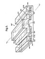
- an alternative optical device of the invention is indicated by 200. It is identical to the device 100 in Figure 2 except that a buried tungsten silicide layer (W Si 2 ) 202 is included between the silicon dioxide layer 102 and the buried contact layer 104, and the layer 104 is selectively doped in regions 204 near the channels 112a, 112b and the rib 108.
- the silicide layer 202 is 100 nm thick.
- the layer 306 has a coefficient of resistivity of less than 1.5 ⁇ m, namely a sheet resistivity of less than 7.5 ⁇ per square when the layer 306 is 200 nm thick.
- the conduction layer 402 and p+ electrode 410 are doped with impurity atoms to a concentration in a range of 10 18 to 10 19 atoms cm -3 .
- the rib 408 is identical in size to the rib 108 illustrated in Figure 3.
- the surface layer 406 is 3.3 ⁇ m thick in regions remote from the rib 408.
- the electrode region 520 is aligned along the axis p-p' and is situated on an opposite side of the central region 516 relative to the p+ electrode 514.
- the rib 512 is a monomode waveguide for confinement of optical radiation of wavelength in a range of 1.3 ⁇ m and 1.5 ⁇ m, in particular radiation of 1.3 ⁇ m and 1.5 ⁇ m wavelength which is often employed in optical communication systems.
- BESOI Biond and Etchback Silicon on Insulator
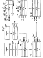
- FIG 8 there is shown schematically stages in a microfabrication process for producing the device 300.
- the couplet 714 is exposed to ion implantation to form a heavily doped p+ surface layer 314 with an impurity to a concentration in a range of 10 18 to 10 19 atoms cm -3 , thereby producing a wafer couplet indicated by 718.
- Standard microfabrication lithographic and dry etching processes are then employed to etch the layers 310, 314 to form a rib 312 in a wafer couplet indicated by 722.
- a dashed line 725 indicates an amount of material removed during formation of the rib 312.
- via channels 316a, 316b are formed by using standard lithographic and etching processes, thereby producing a wafer couplet indicated by 300.
- Further processing stages (not shown) on the couplet 300 include metal track deposition for electrical connection to the n+ doped layer 308 and to the p+ surface layer 314 remaining to provide a completed optical device.
- Such patterning may include regularly spaced isolation channels or holes, namely voids, where the silicide layer 306 has been selectively etched or eroded, for example using ion milling, away.
- the silicide layer 306 may be patterned so that it is incorporated as isolated islands of silicide.
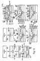
- a doped polysilicon n+ layer 402 is then deposited onto the silicon dioxide layer 404 and into the channel 860.
- An exposed external surface of the layer 402 is then polished to planarise it to form a wafer indicated by 864.
- the wafers 852, 864 are abutted with the surface layer 854 contacting the polysilicon n+ layer 402 and then thermally bonded at a high temperature of 1100 °C in an atmosphere of wet oxygen and nitrogen to form a wafer couplet indicated by 866.
- the atmosphere is created by mixing oxygen, hydrogen and nitrogen gases which spontaneously react at the high temperature to form a gaseous mixture of steam, oxygen and nitrogen.
- the couplet 866 is polished to thin the wafer 856 contained therein to form a layer 406 where a dashed line 870 indicates a quantity of material removed by polishing to form a couplet indicated by 872.
- the layer 406 of the couplet 872 is exposed to boron impurity implantation to form a doped p+ surface layer 874 to provide a wafer couplet indicated by 876.
- the layer 406 is doped with boron impurity to a concentration in a range of 10 18 to 10 19 atoms cm -3 .
- An exposed external surface of the layer 506 is then polished to planarise it to form a wafer indicated by 964.
- the wafers 958, 964 are abutted with the surface layer 504 contacting the polysilicon n+ layer 506 and then, whilst being maintained in contact, thermally bonded at a high temperature of 1100 °C for a period of 60 minutes in an atmosphere of wet oxygen and nitrogen to form a wafer couplet indicated by 966.
- the atmosphere is created by mixing oxygen, hydrogen and nitrogen gases which spontaneously react at the high temperature to form a gaseous mixture of steam, oxygen and nitrogen.
- the couplet 966 is polished to thin the wafer 952 contained therein to form a layer 510 where a dashed line 970 indicates a quantity of material removed by polishing to form a couplet indicated by 972.
- the layer 510 of the couplet 972 is exposed to boron impurity implantation to form a doped p+ surface layer 514 to provide a wafer couplet indicated by 976.
- the layer 510 is doped with boron impurity to a concentration in a range of 10 18 to 10 19 atoms cm -3 .
- the surface layer 514 and the layer 510 are selectively etched back as indicated by a dashed line 978 except in an area to form a rib 512, thereby providing a wafer couplet indicated by 982.
- Two connection via channels 518a, 518b are then delineated and etched through the layers 508, 510, to provide a couplet indicated by 500.
- Further processing stages (not shown) on the couplet 500 include metal track deposition for electrical connection to the n+ layer 504 and to the p+ surface layer 514 remaining to provide a completed optical device.
- the ribs 108, 312, 408, 512 may be gold doped in order to increase device operating bandwidth by ensuring rapid removal of charge carriers by recombination.
- charge carrier recombination within the ribs 108, 312, 408, 512 may be increased by forming lattice defects therein which function as recombination sites. Such defects may be introduced by exposing the ribs 108, 312, 408, 512 to high power laser, electron or hydrogen ion beams.
- the ribs 108, 312, 408, 512 may be exposed to intense neutron beams for introducing the defects.
- the rib 108, 312, 408, 512, 624, 724, 880, 980 incorporates dopant impurity to a concentration of less than 10 16 atoms cm -3 , the concentration may be Increased above 10 16 atoms cm -3 with a consequence that radiation absorption within the device 100, 200, 300, 400, 500 increases correspondingly.
- FIG. 7 to 10 fabrication of single optical devices is illustrated in Figures 7 to 10, it is possible to fabricate a number of devices simultaneously on the wafers 600, 604. 302, 702, 850, 856, 950, 952.
- the devices thereby fabricated may be separated from one another by dicing or sawing the couplets 100, 300, 400, 500, said devices then comprising elements of the wafers 600, 604, 302, 702, 850, 856, 950, 952 which are bonded together.
- an array of the devices 100, 200, 300, 400, 500 may be fabricated on a wafer couplet for providing a phased array device.
- the devices 100, 200, 300, 400, 500 are adapted to modulate radiation, use of high conductivity buried layers, for example metal silicide layers, in other types of semiconductor optical devices, for example high power solid state lasers, is also feasible for providing an electrical path of reduced series resistance for applying bias to said devices.
Landscapes
- Physics & Mathematics (AREA)
- Nonlinear Science (AREA)
- General Physics & Mathematics (AREA)
- Optics & Photonics (AREA)
- Optical Modulation, Optical Deflection, Nonlinear Optics, Optical Demodulation, Optical Logic Elements (AREA)
- Optical Integrated Circuits (AREA)
- Semiconductor Lasers (AREA)
- Optical Communication System (AREA)
- Glass Compositions (AREA)
Claims (31)
- Optische Einrichtung mit einem aktiven Bereich (108; 312; 408; 512) für die Fortleitung von Strahlung und einer Injektionseinrichtung (110; 202, 204; 410, 414; 514, 520) zum Injizieren von Ladungsträgern in den aktiven Bereich, dadurch gekennzeichnet, dass die Injektionseinrichtung eine vergrabene Schicht mit hoher Leitfähigkeit (104; 202; 306; 308; 402; 506) zwischen zwei Waferelementen eines gebondeten Waferpaares enthält, und der leitfähige Bereich (204; 414) der vergrabenen Schicht zur Konzentration von Ladungsträgern in dem aktiven Bereich zwischen dem Rest der vergrabenen Schicht und dem aktiven Bereich liegt.
- Einrichtung nach Anspruch 1, dadurch gekennzeichnet, dass der leitfähige Bereich (414) ein Bereich der vergrabenen Schicht (402) ist, der durch eine Isolierschicht (404) hervorsteht, die sich zwischen Teilen der Einrichtung erstreckt.
- Einrichtung nach Anspruch 2, dadurch gekennzeichnet, dass die vergrabene Schicht eine Polysiliziumschicht (402) ist.
- Einrichtung nach Anspruch 3, dadurch gekennzeichnet, dass die Polysiliziumschicht (402) Störstellen durch Dotierungsmittel in einer Konzentrationen einem Bereich von 1018 bis 1019 Atome cm-3 enthält.
- Einrichtung nach Anspruch 1, dadurch gekennzeichnet, dass der leitfähige Bereich ein stark dotierter Bereich (204) mit anderer chemischer Zusammensetzung als die der vergrabenen Schicht (202) ist.
- Einrichtung nach Anspruch 1 oder 5, dadurch gekennzeichnet, dass die vergrabene Schicht eine Metallsilizidschicht (202) ist.
- Einrichtung nach Anspruch 6, dadurch gekennzeichnet, dass die vergrabene Schicht (202) eine Wolframsilizidschicht ist.
- Einrichtung nach Anspruch 6, dadurch gekennzeichnet, dass die vergrabene Schicht (202) eine der Schichten Tantalsilizidschicht, Kobaltsilizidschicht und Titansilizidschicht ist.
- Einrichtung nach Anspruch 5, dadurch gekennzeichnet, dass der stark dotierte Bereich (204) und die vergrabene Schicht (202) gleichartige Störstellen durch Dotierungsmittel gemeinsam haben, die in der erstgenannten Leitfähigkeit schaffen.
- Einrichtung nach Anspruch 9, dadurch gekennzeichnet, dass die Störstellen durch Dotierungsmittel thermisch von der vergrabenen Schicht (202) zu dem stark dotierten Bereich (204) diffundiert werden können.
- Einrichtung nach Anspruch 9 oder 10, dadurch gekennzeichnet, dass die Konzentration der Störstellen durch Dotierungsmittel in dem stark dotierten Bereich in einem Bereich von 1018 bis 1019 Atome cm-3 liegt.
- Einrichtung nach Anspruch 1, dadurch gekennzeichnet, dass die vergrabene Schicht (708) ein chemisches Element des Materials des Waferpaares (714) enthält.
- Einrichtung nach Anspruch 12, dadurch gekennzeichnet, dass die vergrabene Schicht (202; 708) ein Metallsilizid ist und das Material des Waferpaares Silizium ist.
- Einrichtung nach Anspruch 1, dadurch gekennzeichnet, dass sie eine dielektrische Isolierschicht (304; 504) zur elektrischen Isolation des aktiven Bereichs, der vergrabenen Schicht, der Injektionseinrichtung und des leitfähigen Bereichs von anderen Elementen der Einrichtung enthält.
- Einrichtung nach Anspruch 1, dadurch gekennzeichnet, dass der aktive Bereich Störstellen durch Dotierungsmittel in einer Konzentration von weniger als 1016 Atome cm-3 enthält.
- Optische Einrichtung nach Anspruch 1, dadurch gekennzeichnet, dass der aktive Bereich (108; 312; 407, 512) eine Wellenleitereinrichtung für Strahlung bereitstellt, bei der der Brechungsindex durch die Injektionseinrichtung modulierbar ist.
- Einrichtung nach Anspruch 1, dadurch gekennzeichnet, dass eines der Waferelemente in dem Waferpaar den aktiven Bereich bereitstellt.
- Einrichtung nach Anspruch 1, dadurch gekennzeichnet, dass der leitfähige Bereich eine erste Elektrode (110) umfasst, die an einer Seite des aktiven Bereichs angeordnet ist, und die Einrichtung eine zweite Elektrode (204) enthält, die an der anderen Seite angeordnet ist.
- Einrichtung nach Anspruch 18, dadurch gekennzeichnet, dass die erste Elektrode zwischen dem aktiven Bereich (108) und einer Isolierschicht (102) liegt.
- Einrichtung nach Anspruch 1, dadurch gekennzeichnet, dass der aktive Bereich eine Wellenleitereinrichtung für Strahlung bereitstellt, und die Injektionseinrichtung dazu eingerichtet ist, den Brechungsindex der Wellenleitereinrichtung zu modulieren, indem sie Ladungsträger überwiegend in Bereiche davon injiziert, in denen sich Strahlung überwiegend fortbewegt.
- Einrichtung nach Anspruch 1, dadurch gekennzeichnet, dass die vergrabene Schicht (202) einen Widerstandkoeffizienten von weniger als 1,5 µΩm hat.
- Einrichtung nach Anspruch 1, dadurch gekennzeichnet, dass die vergrabene Schicht (202) einen Widerstandkoeffizienten von weniger als 7,5 Ω/□ hat.
- Einrichtung nach Anspruch 1,21 oder 22, dadurch gekennzeichnet, dass die vergrabene Schicht wenigstens eine der Möglichkeiten Löcher, Insel und Kanäle zum Verringern der Spannung zwischen ihr und der Schicht, auf die sie gebondet ist, enthält.
- Einrichtung nach Anspruch 1, dadurch gekennzeichnet, dass in dem aktiven Bereich wenigstens eine der Möglichkeiten(i) Golddotierung; und(ii) induzierte Gitterdefekte
zur Verringerung der Lebensdauer der Ladungsträger und zur Erhöhung der Dichte der Rekombinationsorte darin enthalten ist. - Verfahren zur Herstellung einer optischen Einrichtung, das die folgenden Schritte umfasst:(a) Bereitstellen von ersten und zweiten Waferelementen (302, 702; 850, 856);(b) Versehen der Waferelemente mit einer Schicht, die strukturiert ist (308, 306, 304; 854, 402, 404), um die Injektionseinrichtung zum Injizieren von Ladungsträgern in einen aktiven Bereich der Einrichtung für die Fortleitung von Strahlung zu definieren;(c) Versehen eines der Waferelemente mit einer Metallsilizidschicht (306) oder einer Polysiliziumschicht (402), um eine Injektionseinrichtung bereitzustellen;(d) Bonden der Waferelemente, um ein Waferpaar (714; 866) herzustellen, innerhalb dessen die Metallsilizidschicht oder die Polysiliziumschicht vergraben ist; und(e) Verarbeiten des Waferpaares (714; 866), um den aktiven Bereich der Einrichtung zu definieren.
- Verfahren nach Anspruch 25, dadurch gekennzeichnet, dass in Schritt (b) die strukturierte Schicht eine Isolierschicht (404) ist, die mit einer Lücke (414) hergestellt wird, und in Schritt (c) die Injektionseinrichtung so ausgebildet wird, dass sie durch die Lücke (414) hervorsteht.
- Verfahren nach Anspruch 25, dadurch gekennzeichnet, dass die Silizidschicht eine Wolframsilizidschicht umfasst.
- Verfahren nach Anspruch 25, bei dem in Schritt (d) die Waferelemente thermisch gebondet werden, indem sie miteinander für eine Zeitdauer in Kontakt gebracht werden, und sie während der Zeitdauer auf eine Temperatur in einem Bereich von 800 °C bis 1200 °C geheizt werden.
- Verfahren nach Anspruch 25, dadurch gekennzeichnet, dass die Silizidschicht (306) selektiv mit Störstellen durch Dotierungsmittel dotiert ist, die von dort in eine angrenzende Schicht (308) diffundieren, wodurch ein leitfähiger Bereich (320b; 320) zum Konzentrieren der Ladungsträgerinjektion in den aktiven Bereich der Einrichtung (324; 312) definiert wird.
- Verfahren nach Anspruch 25, dadurch gekennzeichnet, dass der aktive Bereiche der Einrichtung wenigstens einem der Verfahren Golddotieren oder Bestrahlen unterzogen wurde, um die Dichte der Rekombinationsorte von Ladungsträgern darin zu erhöhen.
- Verfahren nach Anspruch 25, dadurch gekennzeichnet, dass wenigstens eine der Möglichkeiten Löcher, Insel und Kanäle in die Metallsilizidschicht eingebracht ist, um Spannungen zwischen ihr und der Schicht zu verringern, auf die sie gebondet ist.
Applications Claiming Priority (3)
| Application Number | Priority Date | Filing Date | Title |
|---|---|---|---|
| GB9705803 | 1997-03-20 | ||
| GB9705803A GB2323450A (en) | 1997-03-20 | 1997-03-20 | Optical modulator |
| PCT/GB1998/000585 WO1998043128A1 (en) | 1997-03-20 | 1998-02-24 | High conductivity buried layer in optical waveguide |
Publications (2)
| Publication Number | Publication Date |
|---|---|
| EP0968455A1 EP0968455A1 (de) | 2000-01-05 |
| EP0968455B1 true EP0968455B1 (de) | 2008-01-23 |
Family
ID=10809585
Family Applications (1)
| Application Number | Title | Priority Date | Filing Date |
|---|---|---|---|
| EP98907048A Expired - Lifetime EP0968455B1 (de) | 1997-03-20 | 1998-02-24 | Hochleitende vergrabene schicht in einem optischen wellenleiter |
Country Status (10)
| Country | Link |
|---|---|
| US (1) | US6374001B1 (de) |
| EP (1) | EP0968455B1 (de) |
| JP (2) | JP3944246B2 (de) |
| KR (1) | KR20010005523A (de) |
| CN (1) | CN1134692C (de) |
| AT (1) | ATE384974T1 (de) |
| CA (1) | CA2284197C (de) |
| DE (1) | DE69839042T2 (de) |
| GB (1) | GB2323450A (de) |
| WO (1) | WO1998043128A1 (de) |
Cited By (1)
| Publication number | Priority date | Publication date | Assignee | Title |
|---|---|---|---|---|
| EP4446799A1 (de) * | 2023-02-21 | 2024-10-16 | Apple Inc. | Effiziente pin-phasenschieber |
Families Citing this family (55)
| Publication number | Priority date | Publication date | Assignee | Title |
|---|---|---|---|---|
| GB2333851B (en) * | 1999-02-16 | 2000-01-19 | Bookham Technology Ltd | An optical waveguide |
| AUPP930799A0 (en) * | 1999-03-18 | 1999-04-15 | University Of Sydney, The | Optical planar waveguide device and method of its fabrication |
| JP3384447B2 (ja) * | 1999-07-12 | 2003-03-10 | Nec化合物デバイス株式会社 | 吸収型光変調器およびその製造方法 |
| US6351578B1 (en) * | 1999-08-06 | 2002-02-26 | Gemfire Corporation | Thermo-optic switch having fast rise-time |
| CA2365499C (en) | 2000-12-26 | 2011-02-15 | National Research Council Of Canada | High speed and high efficiency si-based photodetectors using waveguides formed with silicides for near ir applications |
| US6890450B2 (en) * | 2001-02-02 | 2005-05-10 | Intel Corporation | Method of providing optical quality silicon surface |
| KR100397609B1 (ko) * | 2001-02-16 | 2003-09-13 | 삼성전기주식회사 | 캐리어 유입 경로의 폭을 임의로 제어할 수 있는 반도체레이저 다이오드 |
| WO2002069004A2 (en) * | 2001-02-22 | 2002-09-06 | Bookham Technology Plc | Semiconductor optical waveguide device |
| US6853773B2 (en) | 2001-04-30 | 2005-02-08 | Kotusa, Inc. | Tunable filter |
| EP2261953A3 (de) * | 2001-05-17 | 2011-05-25 | Optronx, Inc. | Lichtwellenleiter mit zusätzlichen Polysiliziumschichten |
| US7082235B2 (en) * | 2001-09-10 | 2006-07-25 | California Institute Of Technology | Structure and method for coupling light between dissimilar waveguides |
| US7120338B2 (en) * | 2001-09-10 | 2006-10-10 | California Institute Of Technology | Tuning the index of a waveguide structure |
| US6917727B2 (en) * | 2001-09-10 | 2005-07-12 | California Institute Of Technology | Strip loaded waveguide integrated with electronics components |
| GB2383425A (en) * | 2001-12-19 | 2003-06-25 | Bookham Technology Plc | Integrated optical device |
| US6999668B2 (en) * | 2002-01-09 | 2006-02-14 | Matsushita Electric Industrial Co., Ltd. | Method for manufacturing optical waveguide device, optical waveguide device, and coherent light source and optical apparatus using the optical waveguide device |
| US7010208B1 (en) | 2002-06-24 | 2006-03-07 | Luxtera, Inc. | CMOS process silicon waveguides |
| US6882758B2 (en) * | 2002-07-09 | 2005-04-19 | Bookham Technology Plc | Current tuned Mach-Zehnder optical attenuator |
| GB0216143D0 (en) * | 2002-07-12 | 2002-08-21 | Bookham Technology Plc | Semiconductor optical waveguide device |
| US6901911B2 (en) * | 2002-07-31 | 2005-06-07 | Caterpillar Inc | Pump and hydraulic system with low pressure priming and over pressurization avoidance features |
| US20040191564A1 (en) * | 2002-12-17 | 2004-09-30 | Samsung Sdi Co., Ltd. | Donor film for low molecular weight full color organic electroluminescent device using laser induced thermal imaging method and method for fabricating low molecular weight full color organic electroluminescent device using the film |
| US6853793B1 (en) | 2003-02-21 | 2005-02-08 | Kotura, Inc. | Attenuator having reduced optical loss in the pass mode |
| US6970611B1 (en) | 2003-08-27 | 2005-11-29 | Kotura, Inc. | Optical component having reduced interference from radiation modes |
| WO2005082091A2 (en) * | 2004-02-26 | 2005-09-09 | Sioptical, Inc. | Active manipulation of light in a silicon-on-insulator (soi) structure |
| US7315679B2 (en) * | 2004-06-07 | 2008-01-01 | California Institute Of Technology | Segmented waveguide structures |
| US7035487B2 (en) * | 2004-06-21 | 2006-04-25 | Intel Corporation | Phase shifting optical device with dopant barrier |
| DK4008949T3 (da) * | 2004-09-29 | 2024-03-04 | Signify Holding Bv | Belysningsindretning |
| FR2879820B1 (fr) * | 2004-12-16 | 2009-01-16 | Commissariat Energie Atomique | Modulateur a jonction capacitive, jonction capacitive et son procede de realisation |
| US7826688B1 (en) | 2005-10-21 | 2010-11-02 | Luxtera, Inc. | Enhancing the sensitivity of resonant optical modulating and switching devices |
| US7865053B2 (en) * | 2006-12-29 | 2011-01-04 | Alcatel-Lucent Usa Inc. | Multi-semiconductor slab electro-optic modulator and process for using the same |
| JP4495178B2 (ja) * | 2007-02-23 | 2010-06-30 | 日本電信電話株式会社 | シリコン光導波路及びその製造方法 |
| US7672553B2 (en) * | 2007-03-01 | 2010-03-02 | Alcatel-Lucent Usa Inc. | High speed semiconductor optical modulator |
| KR100958718B1 (ko) * | 2007-12-07 | 2010-05-18 | 한국전자통신연구원 | 광신호의 위상을 변환시키는 광전 소자를 포함하는 반도체집적회로 |
| US8213751B1 (en) * | 2008-11-26 | 2012-07-03 | Optonet Inc. | Electronic-integration compatible photonic integrated circuit and method for fabricating electronic-integration compatible photonic integrated circuit |
| CN101813834B (zh) * | 2009-02-19 | 2011-08-24 | 北京大学 | 一种双mos结构硅基电光调制器 |
| WO2010103891A1 (ja) * | 2009-03-13 | 2010-09-16 | 日本電気株式会社 | 光変調器とその製造方法 |
| FR2943802B1 (fr) * | 2009-03-24 | 2011-09-30 | Univ Paris Sud | Modulateur optique a haut debit en semi-conducteur sur isolant |
| US8842942B2 (en) * | 2010-02-08 | 2014-09-23 | Samsung Electronics Co., Ltd. | Optical modulator formed on bulk-silicon substrate |
| GB2477935A (en) * | 2010-02-17 | 2011-08-24 | Univ Surrey | Electro-optic device with a waveguide rib |
| JP5633224B2 (ja) * | 2010-07-22 | 2014-12-03 | 富士通株式会社 | 光半導体装置及びその駆動方法 |
| JP5577909B2 (ja) * | 2010-07-22 | 2014-08-27 | 富士通株式会社 | 光半導体装置及びその製造方法 |
| US20120114001A1 (en) | 2010-11-10 | 2012-05-10 | Fang Alexander W | Hybrid ridge waveguide |
| JP5673060B2 (ja) * | 2010-12-14 | 2015-02-18 | 富士通株式会社 | 光半導体装置及びその製造方法 |
| WO2012124830A1 (ja) * | 2011-03-17 | 2012-09-20 | 日本碍子株式会社 | 光変調素子 |
| US20120280345A1 (en) * | 2011-05-05 | 2012-11-08 | Agency For Science, Technology And Research | Photodetector and a method of forming the same |
| WO2013003830A2 (en) | 2011-06-30 | 2013-01-03 | Saint-Gobain Ceramics & Plastics, Inc. | Abrasive articles including abrasive particles of silicon nitride |
| CN102390803B (zh) * | 2011-08-29 | 2015-02-04 | 常州大学 | 一种高过载、可恢复压力传感器及制造方法 |
| US8989522B2 (en) * | 2012-05-09 | 2015-03-24 | Kotura, Inc. | Isolation of components on optical device |
| US10025120B2 (en) | 2012-12-13 | 2018-07-17 | Luxtera, Inc. | Method and system for a low parasitic silicon high-speed phase modulator having raised fingers perpendicular to the PN junction |
| JP6409299B2 (ja) * | 2014-03-27 | 2018-10-24 | 日本電気株式会社 | 光変調用素子および光変調器 |
| CN105487263B (zh) * | 2014-06-30 | 2018-04-13 | 硅光电科技股份有限公司 | 硅基脊型波导调制器及其制造方法 |
| FR3040499B1 (fr) * | 2015-08-24 | 2017-10-13 | St Microelectronics Crolles 2 Sas | Circuit integre comprenant un dispositif actif de confinement d'un flux lumineux |
| CN111142270B (zh) * | 2018-11-05 | 2022-10-11 | 青岛海信激光显示股份有限公司 | 一种激光散斑消除装置及其激光显示设备 |
| CN111679529B (zh) * | 2020-07-28 | 2024-02-13 | 哈尔滨工业大学(深圳) | 可用于光学相控阵发射单元的长距离亚波长光栅结构 |
| CN114911081B (zh) * | 2022-06-27 | 2025-05-06 | 西安工程大学 | 顶注入电光调制结构 |
| US20240280842A1 (en) * | 2023-02-21 | 2024-08-22 | Apple Inc. | Efficient Pin Phase Shifters |
Family Cites Families (13)
| Publication number | Priority date | Publication date | Assignee | Title |
|---|---|---|---|---|
| US4093345A (en) * | 1976-05-27 | 1978-06-06 | Bell Telephone Laboratories, Incorporated | Semiconductor rib waveguide optical modulator with heterojunction control electrode cladding |
| JPS59181317A (ja) * | 1983-03-31 | 1984-10-15 | Sumitomo Electric Ind Ltd | 光変調素子 |
| US4868633A (en) * | 1986-10-22 | 1989-09-19 | Texas Instruments Incorporated | Selective epitaxy devices and method |
| US4787691A (en) * | 1987-03-26 | 1988-11-29 | The United States Of America As Represented By The Secretary Of The Air Force | Electro-optical silicon devices |
| JPH02228634A (ja) * | 1989-03-01 | 1990-09-11 | Sumitomo Electric Ind Ltd | 半導体光スイッチ及びその製造方法 |
| JPH04107428A (ja) * | 1990-08-28 | 1992-04-08 | Fujikura Ltd | 基板型光スイッチ |
| JPH04179931A (ja) * | 1990-11-14 | 1992-06-26 | Oki Electric Ind Co Ltd | 導波型光デバイス |
| JPH05173199A (ja) * | 1990-12-20 | 1993-07-13 | Fujitsu Ltd | 非線形光学装置 |
| DE4120198A1 (de) * | 1991-06-19 | 1992-12-24 | Bosch Gmbh Robert | Integriert optische schaltung |
| JP2754957B2 (ja) * | 1991-07-10 | 1998-05-20 | 日本電気株式会社 | 半導体光制御素子およびその製造方法 |
| GB2300299B (en) * | 1995-04-26 | 1999-07-07 | Toshiba Cambridge Res Center | Operation of a semiconductor device |
| US5963358A (en) * | 1995-04-26 | 1999-10-05 | Kabushiki Kaisha Toshiba | Semiconductor device and method for its operation |
| JPH08313853A (ja) * | 1995-05-15 | 1996-11-29 | Fujitsu Ltd | 半導体光変調装置、光変調方法及び光半導体装置 |
-
1997
- 1997-03-20 GB GB9705803A patent/GB2323450A/en not_active Withdrawn
-
1998
- 1998-02-24 CN CNB988052830A patent/CN1134692C/zh not_active Expired - Fee Related
- 1998-02-24 JP JP54208598A patent/JP3944246B2/ja not_active Expired - Fee Related
- 1998-02-24 KR KR1019997008581A patent/KR20010005523A/ko not_active Ceased
- 1998-02-24 CA CA002284197A patent/CA2284197C/en not_active Expired - Fee Related
- 1998-02-24 US US09/380,982 patent/US6374001B1/en not_active Expired - Fee Related
- 1998-02-24 DE DE69839042T patent/DE69839042T2/de not_active Expired - Lifetime
- 1998-02-24 EP EP98907048A patent/EP0968455B1/de not_active Expired - Lifetime
- 1998-02-24 AT AT98907048T patent/ATE384974T1/de not_active IP Right Cessation
- 1998-02-24 WO PCT/GB1998/000585 patent/WO1998043128A1/en not_active Ceased
-
2006
- 2006-11-15 JP JP2006308891A patent/JP2007079604A/ja active Pending
Cited By (1)
| Publication number | Priority date | Publication date | Assignee | Title |
|---|---|---|---|---|
| EP4446799A1 (de) * | 2023-02-21 | 2024-10-16 | Apple Inc. | Effiziente pin-phasenschieber |
Also Published As
| Publication number | Publication date |
|---|---|
| EP0968455A1 (de) | 2000-01-05 |
| KR20010005523A (ko) | 2001-01-15 |
| ATE384974T1 (de) | 2008-02-15 |
| DE69839042D1 (de) | 2008-03-13 |
| CA2284197C (en) | 2006-06-06 |
| DE69839042T2 (de) | 2009-02-12 |
| US6374001B1 (en) | 2002-04-16 |
| CN1134692C (zh) | 2004-01-14 |
| GB9705803D0 (en) | 1997-05-07 |
| CN1257586A (zh) | 2000-06-21 |
| CA2284197A1 (en) | 1998-10-01 |
| JP2007079604A (ja) | 2007-03-29 |
| WO1998043128A1 (en) | 1998-10-01 |
| JP3944246B2 (ja) | 2007-07-11 |
| GB2323450A (en) | 1998-09-23 |
| JP2001526797A (ja) | 2001-12-18 |
Similar Documents
| Publication | Publication Date | Title |
|---|---|---|
| EP0968455B1 (de) | Hochleitende vergrabene schicht in einem optischen wellenleiter | |
| US7751654B2 (en) | Electro-optic modulation | |
| US8362494B2 (en) | Electro-optic device with novel insulating structure and a method for manufacturing the same | |
| EP1983359B1 (de) | Optischer wellenleiter | |
| US5908305A (en) | Electro-optic device | |
| US6987910B2 (en) | Silicon light waveguide with MOS capacitors positioned on the waveguide | |
| US8873895B2 (en) | Optical modulator | |
| US7657146B2 (en) | Optoelectric high frequency modulator integrated on silicon | |
| JP2019215488A (ja) | 電気光学変調器 | |
| US8483520B2 (en) | Optical modulation structure and optical modulator | |
| Leonberger et al. | GaAs p+ n− n+ directional‐coupler switch | |
| EP1782123B1 (de) | Mit einem halbleiterwellenleiter vorgesehener optischer hochgeschwindigkeitsphasenschieber | |
| EP0202321B1 (de) | Optische wellenleitungstechnik in einschlussmassen | |
| Li et al. | 2 x 2 optical waveguide switch with bow-tie electrode based on carrier-injection total internal reflection in SiGe alloy | |
| TW445656B (en) | Optical device | |
| EP0447815B1 (de) | Magnetooptisches Gerät | |
| Moselund et al. | Cointegration of gate-all-around MOSFETs and local silicon-on-insulator optical waveguides on bulk silicon | |
| Thomson et al. | Total internal reflection optical switch in SOI with defect engineered barrier region | |
| Atta et al. | Fabrication of a highly efficient optical modulator based on silicon-on-insulator | |
| Dumas | Germanium on silicon photonics | |
| Hsu et al. | Silicon pin optical waveguide modulators fabricated on the silicon and silicon-on-insulator substrates | |
| Ce-zhou et al. | Double-Injection Bifurcation Optical Active Switch Integrated on Silicon-on-Insulator for 1.3 μm Operation | |
| Aronson et al. | Integrated‐optical switch arrays in GaAs based on electrically controlled dynamic free carrier gratings |
Legal Events
| Date | Code | Title | Description |
|---|---|---|---|
| PUAI | Public reference made under article 153(3) epc to a published international application that has entered the european phase |
Free format text: ORIGINAL CODE: 0009012 |
|
| 17P | Request for examination filed |
Effective date: 19990917 |
|
| AK | Designated contracting states |
Kind code of ref document: A1 Designated state(s): AT BE CH DE DK ES FI FR GB GR IE IT LI LU MC NL PT SE |
|
| RAP1 | Party data changed (applicant data changed or rights of an application transferred) |
Owner name: QINETIQ LIMITED |
|
| 17Q | First examination report despatched |
Effective date: 20041104 |
|
| GRAP | Despatch of communication of intention to grant a patent |
Free format text: ORIGINAL CODE: EPIDOSNIGR1 |
|
| GRAS | Grant fee paid |
Free format text: ORIGINAL CODE: EPIDOSNIGR3 |
|
| GRAA | (expected) grant |
Free format text: ORIGINAL CODE: 0009210 |
|
| RBV | Designated contracting states (corrected) |
Designated state(s): AT BE CH DE DK ES FI FR GR IE IT LI LU MC NL PT SE |
|
| AK | Designated contracting states |
Kind code of ref document: B1 Designated state(s): AT BE CH DE DK ES FI FR GR IE IT LI LU MC NL PT SE |
|
| REG | Reference to a national code |
Ref country code: CH Ref legal event code: EP |
|
| REG | Reference to a national code |
Ref country code: IE Ref legal event code: FG4D |
|
| REF | Corresponds to: |
Ref document number: 69839042 Country of ref document: DE Date of ref document: 20080313 Kind code of ref document: P |
|
| REG | Reference to a national code |
Ref country code: CH Ref legal event code: NV Representative=s name: E. BLUM & CO. AG PATENT- UND MARKENANWAELTE VSP |
|
| REG | Reference to a national code |
Ref country code: SE Ref legal event code: TRGR |
|
| PG25 | Lapsed in a contracting state [announced via postgrant information from national office to epo] |
Ref country code: FI Free format text: LAPSE BECAUSE OF FAILURE TO SUBMIT A TRANSLATION OF THE DESCRIPTION OR TO PAY THE FEE WITHIN THE PRESCRIBED TIME-LIMIT Effective date: 20080123 Ref country code: ES Free format text: LAPSE BECAUSE OF FAILURE TO SUBMIT A TRANSLATION OF THE DESCRIPTION OR TO PAY THE FEE WITHIN THE PRESCRIBED TIME-LIMIT Effective date: 20080504 |
|
| PG25 | Lapsed in a contracting state [announced via postgrant information from national office to epo] |
Ref country code: AT Free format text: LAPSE BECAUSE OF FAILURE TO SUBMIT A TRANSLATION OF THE DESCRIPTION OR TO PAY THE FEE WITHIN THE PRESCRIBED TIME-LIMIT Effective date: 20080123 |
|
| ET | Fr: translation filed | ||
| PG25 | Lapsed in a contracting state [announced via postgrant information from national office to epo] |
Ref country code: BE Free format text: LAPSE BECAUSE OF FAILURE TO SUBMIT A TRANSLATION OF THE DESCRIPTION OR TO PAY THE FEE WITHIN THE PRESCRIBED TIME-LIMIT Effective date: 20080123 Ref country code: PT Free format text: LAPSE BECAUSE OF FAILURE TO SUBMIT A TRANSLATION OF THE DESCRIPTION OR TO PAY THE FEE WITHIN THE PRESCRIBED TIME-LIMIT Effective date: 20080623 |
|
| PG25 | Lapsed in a contracting state [announced via postgrant information from national office to epo] |
Ref country code: MC Free format text: LAPSE BECAUSE OF NON-PAYMENT OF DUE FEES Effective date: 20080228 Ref country code: DK Free format text: LAPSE BECAUSE OF FAILURE TO SUBMIT A TRANSLATION OF THE DESCRIPTION OR TO PAY THE FEE WITHIN THE PRESCRIBED TIME-LIMIT Effective date: 20080123 |
|
| PLBE | No opposition filed within time limit |
Free format text: ORIGINAL CODE: 0009261 |
|
| STAA | Information on the status of an ep patent application or granted ep patent |
Free format text: STATUS: NO OPPOSITION FILED WITHIN TIME LIMIT |
|
| 26N | No opposition filed |
Effective date: 20081024 |
|
| PG25 | Lapsed in a contracting state [announced via postgrant information from national office to epo] |
Ref country code: IE Free format text: LAPSE BECAUSE OF NON-PAYMENT OF DUE FEES Effective date: 20080225 |
|
| PGFP | Annual fee paid to national office [announced via postgrant information from national office to epo] |
Ref country code: NL Payment date: 20090217 Year of fee payment: 12 |
|
| PGFP | Annual fee paid to national office [announced via postgrant information from national office to epo] |
Ref country code: CH Payment date: 20090217 Year of fee payment: 12 |
|
| PGFP | Annual fee paid to national office [announced via postgrant information from national office to epo] |
Ref country code: SE Payment date: 20090216 Year of fee payment: 12 Ref country code: IT Payment date: 20090226 Year of fee payment: 12 |
|
| PG25 | Lapsed in a contracting state [announced via postgrant information from national office to epo] |
Ref country code: LU Free format text: LAPSE BECAUSE OF NON-PAYMENT OF DUE FEES Effective date: 20080224 |
|
| REG | Reference to a national code |
Ref country code: NL Ref legal event code: V1 Effective date: 20100901 |
|
| REG | Reference to a national code |
Ref country code: CH Ref legal event code: PL |
|
| EUG | Se: european patent has lapsed | ||
| PG25 | Lapsed in a contracting state [announced via postgrant information from national office to epo] |
Ref country code: LI Free format text: LAPSE BECAUSE OF NON-PAYMENT OF DUE FEES Effective date: 20100228 Ref country code: GR Free format text: LAPSE BECAUSE OF FAILURE TO SUBMIT A TRANSLATION OF THE DESCRIPTION OR TO PAY THE FEE WITHIN THE PRESCRIBED TIME-LIMIT Effective date: 20080424 Ref country code: CH Free format text: LAPSE BECAUSE OF NON-PAYMENT OF DUE FEES Effective date: 20100228 |
|
| PG25 | Lapsed in a contracting state [announced via postgrant information from national office to epo] |
Ref country code: NL Free format text: LAPSE BECAUSE OF NON-PAYMENT OF DUE FEES Effective date: 20100901 |
|
| PG25 | Lapsed in a contracting state [announced via postgrant information from national office to epo] |
Ref country code: IT Free format text: LAPSE BECAUSE OF NON-PAYMENT OF DUE FEES Effective date: 20100224 |
|
| PGFP | Annual fee paid to national office [announced via postgrant information from national office to epo] |
Ref country code: FR Payment date: 20120227 Year of fee payment: 15 |
|
| PGFP | Annual fee paid to national office [announced via postgrant information from national office to epo] |
Ref country code: DE Payment date: 20120221 Year of fee payment: 15 |
|
| PG25 | Lapsed in a contracting state [announced via postgrant information from national office to epo] |
Ref country code: SE Free format text: LAPSE BECAUSE OF NON-PAYMENT OF DUE FEES Effective date: 20100225 |
|
| REG | Reference to a national code |
Ref country code: FR Ref legal event code: ST Effective date: 20131031 |
|
| REG | Reference to a national code |
Ref country code: DE Ref legal event code: R119 Ref document number: 69839042 Country of ref document: DE Effective date: 20130903 |
|
| PG25 | Lapsed in a contracting state [announced via postgrant information from national office to epo] |
Ref country code: FR Free format text: LAPSE BECAUSE OF NON-PAYMENT OF DUE FEES Effective date: 20130228 Ref country code: DE Free format text: LAPSE BECAUSE OF NON-PAYMENT OF DUE FEES Effective date: 20130903 |