EP0971993B1 - Composition conferant une planarite par l'elimination de films metalliques - Google Patents
Composition conferant une planarite par l'elimination de films metalliques Download PDFInfo
- Publication number
- EP0971993B1 EP0971993B1 EP98915203A EP98915203A EP0971993B1 EP 0971993 B1 EP0971993 B1 EP 0971993B1 EP 98915203 A EP98915203 A EP 98915203A EP 98915203 A EP98915203 A EP 98915203A EP 0971993 B1 EP0971993 B1 EP 0971993B1
- Authority
- EP
- European Patent Office
- Prior art keywords
- metal
- pad
- thin film
- particle diameter
- planarizing
- Prior art date
- Legal status (The legal status is an assumption and is not a legal conclusion. Google has not performed a legal analysis and makes no representation as to the accuracy of the status listed.)
- Expired - Lifetime
Links
Images

Classifications
-
- H—ELECTRICITY
- H10—SEMICONDUCTOR DEVICES; ELECTRIC SOLID-STATE DEVICES NOT OTHERWISE PROVIDED FOR
- H10P—GENERIC PROCESSES OR APPARATUS FOR THE MANUFACTURE OR TREATMENT OF DEVICES COVERED BY CLASS H10
- H10P52/00—Grinding, lapping or polishing of wafers, substrates or parts of devices
-
- H—ELECTRICITY
- H10—SEMICONDUCTOR DEVICES; ELECTRIC SOLID-STATE DEVICES NOT OTHERWISE PROVIDED FOR
- H10P—GENERIC PROCESSES OR APPARATUS FOR THE MANUFACTURE OR TREATMENT OF DEVICES COVERED BY CLASS H10
- H10P52/00—Grinding, lapping or polishing of wafers, substrates or parts of devices
- H10P52/40—Chemomechanical polishing [CMP]
- H10P52/403—Chemomechanical polishing [CMP] of conductive or resistive materials
-
- C—CHEMISTRY; METALLURGY
- C09—DYES; PAINTS; POLISHES; NATURAL RESINS; ADHESIVES; COMPOSITIONS NOT OTHERWISE PROVIDED FOR; APPLICATIONS OF MATERIALS NOT OTHERWISE PROVIDED FOR
- C09G—POLISHING COMPOSITIONS; SKI WAXES
- C09G1/00—Polishing compositions
- C09G1/02—Polishing compositions containing abrasives or grinding agents
-
- C—CHEMISTRY; METALLURGY
- C09—DYES; PAINTS; POLISHES; NATURAL RESINS; ADHESIVES; COMPOSITIONS NOT OTHERWISE PROVIDED FOR; APPLICATIONS OF MATERIALS NOT OTHERWISE PROVIDED FOR
- C09K—MATERIALS FOR MISCELLANEOUS APPLICATIONS, NOT PROVIDED FOR ELSEWHERE
- C09K3/00—Materials not provided for elsewhere
- C09K3/14—Anti-slip materials; Abrasives
- C09K3/1454—Abrasive powders, suspensions and pastes for polishing
- C09K3/1463—Aqueous liquid suspensions
-
- Y—GENERAL TAGGING OF NEW TECHNOLOGICAL DEVELOPMENTS; GENERAL TAGGING OF CROSS-SECTIONAL TECHNOLOGIES SPANNING OVER SEVERAL SECTIONS OF THE IPC; TECHNICAL SUBJECTS COVERED BY FORMER USPC CROSS-REFERENCE ART COLLECTIONS [XRACs] AND DIGESTS
- Y10—TECHNICAL SUBJECTS COVERED BY FORMER USPC
- Y10S—TECHNICAL SUBJECTS COVERED BY FORMER USPC CROSS-REFERENCE ART COLLECTIONS [XRACs] AND DIGESTS
- Y10S977/00—Nanotechnology
- Y10S977/70—Nanostructure
- Y10S977/773—Nanoparticle, i.e. structure having three dimensions of 100 nm or less
- Y10S977/775—Nanosized powder or flake, e.g. nanosized catalyst
-
- Y—GENERAL TAGGING OF NEW TECHNOLOGICAL DEVELOPMENTS; GENERAL TAGGING OF CROSS-SECTIONAL TECHNOLOGIES SPANNING OVER SEVERAL SECTIONS OF THE IPC; TECHNICAL SUBJECTS COVERED BY FORMER USPC CROSS-REFERENCE ART COLLECTIONS [XRACs] AND DIGESTS
- Y10—TECHNICAL SUBJECTS COVERED BY FORMER USPC
- Y10S—TECHNICAL SUBJECTS COVERED BY FORMER USPC CROSS-REFERENCE ART COLLECTIONS [XRACs] AND DIGESTS
- Y10S977/00—Nanotechnology
- Y10S977/84—Manufacture, treatment, or detection of nanostructure
- Y10S977/888—Shaping or removal of materials, e.g. etching
Definitions
- the present invention relates to a planarization composition which is particularly useful for thinning, polishing and planarizing integrated circuitry deposited on semiconductor wafers which have had at least one metal conducting film deposited on their surfaces.
- the thinning, polishing and planarizing serves to remove the metal film.
- the invention also relates to a thinning, polishing and planarizing apparatus and to a method for carrying out the thinning, polishing and planarizing operation.
- a hard material for example a metal or metal nitride such as tungsten, titanium, titanium/tungsten or titanium nitride
- the deposited material filling holes which extend into the body of an insulating thin film and provide an electrical conducting path from the semiconducting or conducting layer under the insulating surface or conductor to a distance above the surface.
- the deposited material constitutes what is commonly referred to as a via, plug, trench or contact.
- the removal of layers of this nature is generally carried out by a thinning, polishing and planarizing operation utilizing a hard surface of a polishing pad and a polishing slurry which wets the pad and is frictionally moved against the excess deposited metal surface to be removed.
- the slurry generally includes alumina particles as the abrasive material along with a liquid chemical carrier and reactant. Basically, the alumina and the chemical carrier are respectively hard and reactive enough so as to abrade away the excess deposited metal which has been deposited on the insulating surface when forming the vias, plugs or contact regions.
- CMP chemical mechanical polishing
- an abrasive material generally alumina or silica
- a liquid carrier and a compound which is corrosive or oxidative toward or will dissolve the substrate.
- U.S. Patent No. 5,391,258 of Brancaleoni, et al. discusses such a process for enhancing the polishing rate of silicon, silica or silicon-containing articles including composites of metals and silica.
- the composition includes an oxidizing agent along with an anion which suppresses the rate of removal of the relatively soft silica thin film.
- the suppressing anion may be any of a number of carboxylic acids.
- Alumina is used as the abrasive material.
- Such particles are not, however, abrasive enough to be used to effectively polish off the above mentioned materials such as tungsten, titanium or titanium nitride.
- colloidal silica which has a pH above 7, and in the absence of an oxidizing agent, is not capable of effectively, i.e., at an acceptably great rate, thinning and planarizing metal or metal nitrides.
- the pH is above 7, the exposed silica would be preferentially etched while the metal and metal nitride layers, relatively speaking, remain un-thinned and un-planarized. Substantial and undesirable dishing of the silicon dioxide would occur around the metal and metal nitride plugs, vias, etc.
- U.S. Patent No. 5,376,222 discloses the use of colloidal silica in an alkaline solution for polishing a silica film on a semiconductor.
- the polishing solution includes a cation of an alkali metal, an alkaline earth, or an ammonium ion.
- the preferred composition includes sodium or potassium ion.
- the slurry is not used to remove metals but only silica.
- U.S. Patent No. 3,877,183 discloses the use of precipitated silicates and/or silicofluorides as polishing substances for semiconductor materials. These polishing substances are utilized to polish the semiconductor, namely, silicon.
- polishing materials such as metals and metal nitrides and silicon dioxide insulating layers so as to remove them at sufficient rates and selectivities.
- the resulting excess metal conducting film on the exposed doped oxide surface of the wafer must be polished away, thinned and planarized without appreciably thinning and planarizing the newly exposed doped or undoped silicon dioxide. It is desirable to stop the thinning and planarizing process once the excess metals and metal nitride have been polished away thus exposing the underlying doped silicon dioxide layer.
- thinning and planarizing At the start of a typical prior art thinning and planarizing (CMP) process, one metal layer is exposed. After a substantial amount of thinning and planarization, a second metal nitride layer, a third metal layer and a silicon dioxide layer are exposed to the thinning and planarizing process.
- CMP thinning and planarizing
- the conventional alumina-based thinning and planarizing process which includes, intermixed with the alumina abrasive, an acidic liquid system and an oxidizer, each exposed metal and metal nitride thins and planarizes at a different rate.
- the most widely used slurry system thins and planarizes the second exposed metal, the titanium so-called “glue” layer, at a substantially different rate than other exposed metal (tungsten) and metal nitride (titanium nitride) layers.
- the result is a less planar surface than is desired by the integrated circuit device manufacturer.
- the polishing process "stops", or slows down, to a polishing rate 1/6 the rate prior to this metal layer. To date, there has not been a satisfactory solution to this problem.
- the present invention is directed to overcoming one or more of the problems as set forth above.
- a planarization composition is set forth in accordance with an embodiment of the invention.
- the composition comprises spherical silica particles having a silica particle concentration of 0.5 to 30 weight percent, a weight average particle diameter which falls within the range from about 0.03 ⁇ m to about 2 ⁇ m, and is mono-disperse in that at least about 90 weight percent of the particles have a variation in particle diameter from the average particle diameter of no more than about ⁇ 20%.
- a liquid carrier comprising up to 20 weight percent ROH, and an amine hydroxide which is NR 4 OH or NR 2 NR 3 OH, where each R is any one of H, CH 3 , CH 2 CH 3 , C 3 H 7 or C 4 H 9 , in the amount of 0.1 to 10 weight percent; an oxidizer which is in the amount from about 0.5 to 15 weight percent; an acid stabilizer for adjusting the pH to fall within a range from about 7.0 to about 0.5; and the remainder is water.
- a secondary planarization composition is set forth in accordance with an embodiment of the invention.
- the composition comprises spherical silica particles having a silica particle concentration of 0.5 to 15 weight percent, a weight average particle diameter which falls within the range from about 0.03 micron to about 2 micron, and is mono-disperse in that at least about 90 weight percent of the particles have a variation in particle diameter from the average particle diameter of no more than about +/-15%.
- a liquid carrier comprising up to 45 weight percent ROH, and an amine hydroxide which is NR 4 OH or NR 2 NR 3 OH, where each R is any one of H, CH 3 , CH 2 CH 3 , C 3 H 7 or C 4 H 9 , in the amount of 0.1 to 10 weight percent and the rest is water.
- a pad which is wet with the above planarization composition is set forth.
- Yet another embodiment of the invention is a method of planarizing a substrate having a hard metal, metal nitride or insulating surface coating to remove the coating.
- the method comprises positioning the planarization composition set forth above between a pad and the surface coating and rubbing the pad against the surface coating until the surface coating has been removed.
- the materials utilized are all of ultra-pure quality whereby the suspension has a total metals content of no more than about 3,000 parts per billion by weight.
- Yet another embodiment of the invention is a method for manufacturing inter-dielectric and inter-metal layer vias and plugs.
- An insulating layer thin film is deposited onto a surface of a substrate.
- One or more small holes defined by respective sidewalls and bottoms are etched into the film and extend to at least the substrate surface.
- a first metal thin film is introduced onto the insulating thin film top surface and onto the respective sidewalls and bottoms to coat the insulating layer thin film and respective sidewalls and bottoms formed, without filling the holes, thereby forming a first metal surface.
- a first metal nitride thin film is deposited onto the first metal surface in such a manner that it coats the holes and forms a first metal nitride surface.
- a second metal film is deposited onto the first metal nitride surface in such a manner that it fills the holes and forms a second metal surface.
- a planarizing composition as set forth above is positioned between the second metal surface and a pad. The pad is rubbed against the second metal surface sufficiently to thin and planarize the first metal thin film, the first metal nitride thin film, and the second metal film.
- an oxidizer which is useful for oxidizing the hard materials which are to be removed by converting them into materials which can be removed by the relatively soft and uniform silica particles, the ability has been gained to very controllably polish hard materials and to end up with a resultant polished surface which is highly planar.
- an oxidizer is also present, as it preferably is, it serves to accelerate the removability of the oxidized compound resulting from reaction of the hard material with the oxidizers.
- results obtained have been thinning and planarization rates over twice the conventional rates, one-half the surface roughness levels, substantially reduced wafer non-uniformity, one-tenth the scratch density and a substantial reduction of the post-CMP particle and residue levels encountered after thinning with the conventional alumina-based slurry.
- such common via materials as titanium, titanium/tungsten, titanium nitride and tungsten, as well as insulative silicon dioxide, can be removed at controlled rates to provide a planar surface of improved planarity.
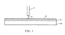
- FIG. 1 illustrates a schematic view of a pad 10 being wet with the planarization composition 8 of the present invention.
- the planarization composition 8 forms a planarization composition thin film 6 on the top surface of the pad 10 to thereby wet the pad 10.
- a delivery system 7 brings the planarization composition 8 above the pad 10 which is located on a surface of the polishing platen 60.
- Another method of wetting the pad 10 includes a holed platen (not shown) having holes (not shown) from the top surface of the platen to the bottom surface of the platen.
- the planarization composition 8 would then be introduced from the bottom surface of the pad 10 through the bottom surface of the holed platen (not shown) to form a uniform planarization composition thin film. It is understood that either method to wet the pad 10 may be used, or any other method that results in a pad 10 with a uniform planarization composition thin film.
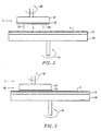
- Figure 2 illustrates a schematic view of the pad 10 in accordance with an embodiment of the present invention wet by the planarization composition (not shown) to form the planarization film 6.
- a quill 40 rotating in a wafer rotating direction 80, holds wafer 30 in the pre-rubbing position 5 to lower the quill 40 and wafer 30 in the rubbing direction 50 towards the pad 10.
- the pad 10 is supported by polishing platen 60 and rotates in a pad rotating direction 70.
- the pad 10 is used to thin, polish and planarize the hard flat surface layer 20 of a partially fabricated integrated circuit (not shown) on wafer 30.
- Figure 3 illustrates a rubbing position 90 of the quill 40 and wafer 30 downwardly relative to the pre-rubbing position 5 of Fig. 2.
- the pad 10 wet with the planarization composition to form the planarization composition thin film 6 rubs against the hard flat surface layer 20 of the wafer 30 to provide the desired thinning, polishing and planarizing of the hard flat surface layer 20.
- the pad 10 has been wet by a planarization composition with a composition as follows.
- a planarization composition which comprises from about 0.5 to about 30 weight percent of spherical, mono-dispersed silica particles.
- the particles have a weight average particle diameter which falls within the range from about 0.03 ⁇ m to about 2 ⁇ m. More preferably, the weight average particle diameter falls within the range from about 0.03 ⁇ m to about 0.4 ⁇ m.
- the particles are mono-disperse, that is, at least about 90 weight percent of the particles have a variation in particle diameter from the weight average particle diameter of no more than about ⁇ 20%, preferably less than ⁇ 15%. This is a critical requirement of the particles.
- the spherical silica particles in accordance with the present invention can be made in the manner discussed and set forth in previous mentioned U.S. Patent No. 4,842,837.
- the composition further comprises a liquid carrier comprising up to 20 weight percent ROH, and an amine hydroxide which is NR 4 OH or NR 2 NR 3 OH, where each R is any one of H, CH 3 , CH 2 CH 3 , C 3 H 7 or C 4 H 9 , in the amount of 0.1 to 10 weight percent; an oxidizer which is in the amount from about 0.5 to 15 weight percent; an acid stabilizer for adjusting the pH to fall within a range from about 7.0 to about 0.5; and the remainder is water.
- Figure 4 illustrates an embodiment of the present invention depicting a cross-sectional view of a sample semiconductor device 100 made using the method for manufacturing an inter-dielectric and inter-metal layer vias and plugs of the present invention.
- An insulating layer thin film 110 on substrate 120 has been etched to form a hole 130 formed by sidewalls 140 and bottom 150. Etching is performed using any one of many conventional methods. It is understood that while Figure 4 depicts a single hole 130 for a sample semiconductor device 100, the present invention extends to more than one sample semiconductor device and may have numerous holes.
- the insulating film 110 is generally a doped or undoped silicon dioxide but may be a polyamide, Teflon, boron nitride, spin-on-glass (SOG), FSG, or N-Parylens.
- a first metal thin film 160 is deposited on top of the insulating layer thin film 110 and along sidewalls 140 and bottom 150. The first metal thin film 160 merely coats the insulating film 110 and hole 130, sidewalls 140 and bottom 150, rather than filling the entire hole 130.
- the first metal thin film 160 is preferably titanium, while tungsten or any other metal of similar properties may also be used.
- the first metal thin film 160 forms a first metal surface 170.
- first metal nitride thin film 180 On top of the first metal surface 170 is a first metal nitride thin film 180 that coats the first metal surface 170 and forms a first metal nitride surface 185.
- a second metal film 190 is then placed on top of the first metal nitride surface 185.
- the second metal film 190 may be either titanium or tungsten or any other metal having similar properties to these two metals. While the first metal thin film 160 and first metal nitride thin film merely coat the respective surface below each, the second metal film 190 fills the hole 130 and forms a second metal surface 200.
- first metal thin film 160 In use, it is desirable to remove by polishing, thinning and planarizing the first metal thin film 160, the first metal nitride thin film 180 and the second metal film 190 to expose only the underlying insulating layer thin film 110 (generally doped silicon dioxide) as shown in Figure 5.
- insulating layer thin film 110 generally doped silicon dioxide
- Planarizing is accomplished by positioning the planarization composition described above between the pad 10 against a solid surface coating of the wafer 20 of Fig. 2.
- the solid surface coating would include the second metal thin film 190, the first metal nitride thin film 180 and the first metal thin film 160 of Fig. 4, with the second metal surface 200 contacting the pad 10 wet with the aforementioned composition.
- the pad 10 is rubbed against the second metal surface 200 due to the rotating of the wafer 20 and the pad 10 and the perfectly planar surface 210 of Fig. 5 is accomplished.
- a secondary planarization process known as "buff polish" is sometimes necessary after the method of planarizing described above is completed.
- the secondary planarization process is used when the roughness of the resultant insulating layer thin film 110 of Fig. 5 is not satisfactory or if it is necessary to remove strongly held slurry composition remnants. Certain factors, such as the use of ferric nitrate as an oxidizer in the planarization process above, causes the surface of the exposed insulating thin layer 110 to be too rough and therefore the secondary planarization is needed.
- the roughness (variance is surface coating) of the insulating film 110 should be less than about 10 angstroms, otherwise the secondary planarization process is needed.
- a secondary planarization process may be needed when additional factors, other than using a ferric nitrate oxidizer in the planarization composition above (see Example 1 below), causes the surface roughness of the insulating layer thin film 110 to be too rough, i . e . greater than 10 angstroms.
- the secondary planarization process uses a secondary planarization composition comprising spherical silica particles having a silica particle concentration of 0.5 to 15 weight percent, a weight average particle diameter which falls within the range from about 0.03 micron to about 2 micron, and is mono-dispersed in that at least about 90 weight percent of the particles have a variation in particle diameter from the average particle diameter of no more than about +/-15%.
- a liquid carrier comprising up to 45 weight percent ROH, and an amine hydroxide which is NR 4 OH or NR 2 NR 3 OH, where each R is any one of H, CH 3 , CH 2 CH 3 , C 3 H 7 or C 4 H 9 , in the amount of 0.1 to 10 weight percent and the rest is water.
- the specific method of formulating the silica particles which is currently preferred is to add tetraethylorthosilicate (TEOS) to an ammonium hydroxide solution in water having a pH of approximately 9.0-12.0.
- TEOS tetraethylorthosilicate
- the products formed by the reaction include the silica particles of the desired size, ammonia, ammonium ions and ethanol. What results is a suspension of spherical silica particles in an ethanol/ammonium hydroxide solution.
- the reaction can be varied somewhat.
- the TEOS can be replaced with a tetraalkylorthosilicate when the alkyl group comprises methyl, propyl or butyl radicals. If this is done the product is not ethanol but instead the corresponding alcohol.
- the ammonium hydroxide can be replaced by compounds of the formulas NR 4 OH, and/or NR 2 NR 3 OH wherein each R is any one of CH 3 , CH 2 CH 3 , C 3 H 7 or C 4 H 9 .
- the amine hydroxide constituent of the nature defined above will usually be present in the amount from about 0.1% to about 10% weight percent.
- the alcohol constituent will comprise from up to about 20% of the resulting planarization composition, all percents herein being by weight.
- any of a number of oxidizers can be included with the liquid carrier. Particularly desirable are such oxidizers as hydrogen peroxide, potassium iodate, ferric nitrate, ferric cyanide, sodium iodate, and peroxyacetic acid.
- the oxidizer is generally present in an amount from about 0.5% to about 15%, more preferably from about 3% to about 13%. The remainder of the composition is water. The total amount of water will not exceed about 70%.
- the pH is adjusted to fall within a range from about 0.5 to about 7, more preferably about 0.5 to about 6.
- the pH is preferably adjusted such that the rate of removal of the oxide formed due to the oxidation reaction between the oxidizer and the metal and metal nitride surface coatings are adjusted to a desired substantially equivalent rate.
- a desired equivalent rate is meant a rate such that the coating can be removed in a relatively short time and at a rate substantially equivalent for each metal and metal nitride being removed.
- the amount of the oxidizer and the pH are selected such that surface polishing rate of the following materials, which are often used for forming vias, are as follows:
- the pH adjustment will be such as to adjust the pH to be in the acidic range generally in the range from below 7 to about 0.5, preferably from about 4 to about 1. This will provide the necessary acidity. It is not desirable to make the composition too acidic as the vias may then be attacked and the oxidation rate may be too fast.
- Suitable acids which may be used to adjust the pH include inter alia , acetic, acetylsalicylic and other carboxylic acids, dicarboxylic acids, citric acid, nitric acid, sulfuric acid and hydrochloric acid.
- the ammonium hydroxide has five components:
- the hydrogen peroxide will react with NH 3 (aq) to produce
- nitrate ion can add the following:
- the temperature for the thinning, polishing and planarizing operation will generally fall within a non-critical range from about 20°C to about 80°C. Indeed, the operation is generally initially at about 20-50°C but the temperature of the surface and the liquid carrier goes up as friction takes place.
- the materials utilized are all of ultrapure quality whereby the suspension has a total metals content of no more than about 3,000 parts per billion by weight. This is particularly useful in the semiconductor processing industries since even small amounts of metal can cause errors in devices thereby cutting down on throughput.
- a planarization composition is formed using an ethyl silicate slurry having a content by weight percent of the following components: Component Weight % Ammonium hydroxide 9.0 ETOH 42.0 SiO 2 12.0
- the pH of the ethyl silicate slurry was approximately 12.0 and the particle size was 188 nm +/- 13.5%.
- Ferric Nitrate and nitric acid are added to the ethyl silicate slurry in a volumetric ratio of 4:1:4.
- the resultant planarizing composition set forth above is placed between a pad and the surface coating having the following .
- the polishing pad was a Thomas West TWI C-22 pad.
- the example comprises positioning the planarizing composition set forth above between a pad and the surface coating and rubbing the pad against the surface coating according to the following planarizing parameters: Parameter Downward Force 7 psi Back Pressure 0 psi Table Speed 120 rpm Quill Speed 80 rpm Planarizing Time 70 seconds
- a secondary planarization process was implemented after the first planarization process.
- the second planarization process is typically called a "buff polish.”
- a second planarization composition was used which consisted of the same ethyl silicate slurry and ultra-high purity (UHP D.I.) water at a volumetric ratio of 1:4, respectively.
- a secondary planarization composition is set forth in accordance with an embodiment of the invention.
- the composition comprises spherical silica particles having a silica particle concentration of 0.5 to 15 weight percent, a weight average particle diameter which falls within the range from about 0.03 micron to about 2 micron, and is mono-disperse in that at least about 90 weight percent of the particles have a variation in particle diameter from the average particle diameter of no more than about +/-15%.
- a liquid carrier comprising up to 45 weight percent ROH, and an amine hydroxide which is NR 4 OH or NR 2 NR 3 OH, where each R is any one of H, CH 3 , CH 2 CH 3 , C 3 H 7 or C 4 H 9 , in the amount of 0.1 to 10 weight percent and the rest is water.
- the buff polish comprises positioning the second planarizing composition set forth above between a pad and the surface coating and rubbing the pad against the surface coating according to the following planarizing parameters: Parameter Downward Force 7 psi Back Pressure 0 psi Table Speed 120 rpm Table Temperature 50° C Quill Speed 80 rpm Planarizing Time 30 seconds
- the buff polish smooths the oxide surface without planarizing further the planarized tungsten/titanium nitride/titanium holes.
- the oxide surface roughness improves from 20-30 angstroms Root-Mean-Square ("RMS") to less than ten angstroms.
- RMS Root-Mean-Square
- the same Thomas West TWI-C22 pad was used for the buff polish.
- the planarizing equipment used was a Strasbaugh 6EC single head polisher.
- a planarization composition is formed using an ethyl silicate slurry having a content by weight percent of the following components: Component Weight % Ammonium hydroxide 8.5% ETOH 47.1% SiO 2 11.8%
- the pH of the ethyl silicate slurry was approximately 12.1 and the particle size was 323 +/- 20.0%. Hydrogen Peroxide and Acetic Acid are added to the ethyl silicate slurry in a volumetric ratio of 2:1:1.
- the resultant planarizing composition set forth above between a pad and the surface coating having the following composition: Surface Coatings Thickness Tungsten 6,000 Titanium 500 Titanium Nitride 500 Oxide 13,000
- the polishing pad was a Rodel Suba-500 pad.
- the example comprises positioning the planarizing composition set forth above between a pad and the surface coating and rubbing the pad against the surface coating according to the following planarizing parameters: Parameter Downward Force 9 psi Back Pressure 0 psi Table Speed 120 rpm Quill Speed 120 rpm Planarizing Time 175 seconds
- a secondary planarization process was not necessary as was in Example 1 because the oxide surface roughness after the primary planarization process was less than 6.0 angstroms RMS.
- a planarization composition is formed using an ethyl silicate slurry having a content by weight percent of the following components: Component Weight % Ammonium hydroxide 9.0 ETOH 42.0 SiO 2 13.1
- the pH of the ethyl silicate slurry was approximately 12.1 and the particle size was 188 +/- 13.5%. Hydrogen Peroxide and Acetic Acid are added to the ethyl silicate slurry in a volumetric ratio of 1:1:1.
- the resultant planarizing composition set forth above was between a pad and the surface coating having the following composition: Surface Coatings Thickness Tungsten 6,000 Titanium 500 Titanium Nitride 500 Oxide 13,000
- the polishing pad was a Rodel IC1000-2A pad.
- the example comprises positioning the planarizing composition set forth above between a pad and the surface coating and rubbing the pad against the surface coating according to the following planarizing parameters: Parameter Downward Force 7 psi Back Pressure 0 psi Table Speed 120 rpm Quill Speed 80 rpm Planarizing Time 120 seconds
- the measured planarization rate was calculated to be 3,469 angstroms per minute.
- the within wafer nonuniformity was 1.0%.
- the selectivity of the tungsten/titanium nitride/titanium surface coating during the planarization process was measured to be 1:1:1.
- a secondary planarization process was not necessary as was in Example 1 because the oxide surface roughness after the primary planarization process was less than 8 angstroms RMS.
- Ethyl silicate slurry having a content by weight percent of the following components: Component Weight % Ammonium hydroxide 6.0 ETOH 38.0 SiO 2 13.0
- the pH of the ethyl silicate slurry was approximately 11.5 and the particle size was 188 nm+/-13.5%.
- Ferric Nitrate and nitric acid are added to the ethyl silicate slurry in a volumetric ratio of 4:1:4.
- the resultant planarizing composition set forth above is placed between a pad and the surface coating having the following composition: Surface coatings Thickness (A) Tungsten 6,000 Titanium nitride 500 Oxide 13,000 In this example there was not a titanium layer present.
- the polishing pad was a Thomas West TWI C-22 pad.
- the example comprises positioning the planarizing composition set forth above between a pad and the surface coating and rubbing the pad against the surface coating according to the following planarizing parameters: Parameter Downward Force 7 psi Back pressure 0 psi Table Speed 120 rpm Quill speed 80 rpm Planarizing time 70 seconds
- a secondary planarization process was implemented after the first planarization process.
- the second planarization process is typically called a "buff polish".
- a second planarization composition was used which consisted of the same ethyl silicate slurry and UHP D.I. water at a volumetric ratio of 1:4 respectively.
- the secondary planarization composition is set forth in accordance with an embodiment of the invention.
- the composition comprises spherical silica particles having a silica particle concentration of 0.5 to 15 weight percent, a weight average particle diameter which falls within the range from about 0.03 micron to about 2 micron, and is mono-disperse in that at least about 90 weight percent of the particles have a variation in particle diameter from the average particle diameter of no more than about +/-15%.
- a liquid carrier comprising up to 45 weight percent ROH, and an amine hydroxide which is NR 4 OH or NR 2 NR 3 OH, where each R is any one of H, CH 3 , CH 2 CH 3 , C 3 H 7 or C 4 H 9 , in the amount of 0.1 to 10 weight percent and the rest is water.
- the buff polish comprises positioning the second planarizing composition set forth above between a pad and the surface coating and rubbing the pad against the surface coating according to the following planarizing parameters: Parameter Downward force 7 psi Back pressure 0 psi Table speed 120 rpm Table temperature 50° C Quill speed 80 rpm Planarizing time 60 seconds
- the buff polish smoothes the oxide surface without planarizing further the planarized tungsten/titanium nitride/titanium holes.
- the oxide surface roughness improves from 20-30 angstroms RMS to less than seven angstroms.
- the same Thomas West TWI-C22 pad was used for the buff polish.
- the planarizing equipment used was a Strasbaugh 6EC single head polisher.
- the present invention provides a composition, article of manufacture and method for carrying out CMP operations to remove such materials as titanium, titanium nitride and tungsten from the surfaces of semiconductor wafers following the deposition of such materials into holes to form vias, contacts and plugs from one level of the semiconductor device to another.
- the method of the present invention provides a much more uniformly planarized surface than can be obtained by prior art methods. This is extremely important to the semiconductor industry wherein extreme precision on a nanometer scale is essential.
Landscapes
- Chemical & Material Sciences (AREA)
- Organic Chemistry (AREA)
- Engineering & Computer Science (AREA)
- Materials Engineering (AREA)
- Mechanical Treatment Of Semiconductor (AREA)
- Detergent Compositions (AREA)
Claims (12)
- Composition conférant une planarité ayant un pH d'environ 0,5 à environ 7, comprenant :où chaque R est l'un quelconque parmi H, CH3, CH2CH3, C3H7 et C4H9.d'environ 0,5 à 30 % en poids de particules de silice sphériques ayant un diamètre de particule moyen en poids qui se situe dans une fourchette d'environ 0,03 µm à environ 2 µm et est mono-dispersée en ce qu'au moins environ 90 % en poids des particules ont une variation du diamètre de particule par rapport au diamètre de particule moyen en poids de pas plus qu'environ ± 20 % ; etun porteur liquide comprenant jusqu'à environ 20 % en poids de ROH ; environ 0,1 à 10 % en poids d'un hydroxyde d'amine sélectionné parmi NR4OH et NR2NR3OH ; un oxydant qui est présent en une quantité située entre 0,5 et 15 pour cent en poids ; un stabilisant acide afin d'ajuster le pH de sorte qu'il se situe dans la fourchette d'environ 0,5 à environ 7 ; le reste étant de l'eau ;
- Composition conférant une planarité selon la revendication 1, dans laquelle l'oxydant est sélectionné parmi le peroxyde d'hydrogène, l'iodate de potassium, le nitrate ferrique, le cyanure ferrique, l'iodate de sodium et l'acide peroxyacétique.
- Composition conférant une planarité selon la revendication 2, dans laquelle la quantité d'oxydant et le pH sont sélectionnés de telle sorte que, lorsqu'elle est utilisée, la composition soit capable de polir une surface de tungstène, de nitrure de titane ou de titane à un rythme de 2000 Å à 6000 Å par minute.
- Composition conférant une planarité selon l'une quelconque des revendications 1 à 3, caractérisée en ce qu'elle présente une teneur totale en métaux dissous de pas plus que 3000 parties par milliard en poids.
- Procédé de préparation d'une composition conférant une planarité selon la revendication 1 comprenant :l'addition d'un tétraalkylorthosilicate dans lequel l'alkyle est le méthyle, l'éthyle, le propyle ou le butyle à une solution dans de l'eau d'un hydroxyde d'amine sélectionné parmi NR4OH et NR2NR3OH où chaque R est l'un quelconque parmi H, CH3, CH2CH3, C3H7 et C4H9, ladite solution ayant un pH d'approximativement 9,0 à 12,0 ;l'inclusion d'un oxydant et, si on le souhaite, d'un stabilisant acide afin d'ajuster le pH de sorte qu'il se situe dans une fourchette d'environ 0,5 à environ 7.
- Procédé selon la revendication 5, dans lequel l'oxydant est sélectionné parmi le peroxyde d'hydrogène, l'iodate de potassium, le nitrate ferrique, le cyanure ferrique, l'iodate de sodium et l'acide peroxyacétique.
- Procédé selon la revendication 5, dans lequel le stabilisant acide est sélectionné parmi les acides acétique, acétylsalicylique et d'autres acides carboxyliques, les acides dicarboxyliques, l'acide citrique, l'acide nitrique, l'acide sulfurique et l'acide chlorhydrique.
- Deuxième composition conférant une planarité comprenant :où chaque R est l'un quelconque parmi H, CH3, CH2CH3, C3H7 et C4H9.d'environ 0,5 à 15 % en poids de particules de silice sphériques ayant un diamètre de particule moyen en poids qui se situe dans une fourchette d'environ 0,03 µm à environ 2 µm et est monodispersée en ce qu'au moins environ 90 % en poids des particules ne présentent pas de variation du diamètre de particule par rapport au diamètre de particule moyen en poids de plus d'environ ± 15 % ; etun porteur liquide comprenant jusqu'à environ 45 % en poids de ROH ; de 0,1 à 10 % en poids d'un hydroxyde d'amine sélectionné parmi NR4OH et NR2NR3OH ; le reste étant de l'eau ;
- Procédé conférant une planarité à un substrat ayant un revêtement de surface solide afin d'éliminer le revêtement comprenant les étapes consistant à :(a) placer une composition selon l'une quelconque des revendications 1 à 4 entre un tampon et le revêtement de surface ; et à(b) frotter le tampon contre le revêtement de surface jusqu'à ce que le revêtement de surface ait été éliminé.
- Procédé selon la revendication 9 comprenant encore les étapes consistant à :(c) placer une deuxième composition conférant une planarité selon la revendication 8 entre le tampon et la surface ; et à(d) frotter le tampon contre la surface jusqu'à ce que la rugosité de la surface ait été réduite à moins 10 Å.
- Procédé de fabrication de fiches et de trous revêtus de couches intermédiaires diélectriques et métalliques comprenant les étapes consistant à :(a) déposer un film mince de couche isolante ayant une surface supérieure sur une surface d'un substrat ;(b) graver un ou plusieurs petits trous définis par des parois latérales et fonds respectifs dans le film et s'étendent au moins jusqu'à la surface du substrat ;(c) introduire un premier film mince métallique sur la surface supérieure du film mince isolant et sur les parois latérales et fonds respectifs sans remplir les trous, formant ainsi une première surface métallique ;(d) déposer un premier film mince de nitrure métallique sur la première surface métallique de telle sorte que le premier film mince de nitrure métallique recouvre les trous et forme une première surface de nitrure métallique ;(e) déposer un deuxième film mince métallique sur la première surface de nitrure métallique de telle sorte que le deuxième film métallique remplisse les trous et forme une deuxième surface métallique ;(f) positionner une composition conférant une planarité selon l'une quelconque des revendications 1 à 3 entre la deuxième surface métallique et une pastille ; et(g) frotter suffisamment le tampon contre la deuxième surface métallique pour amincir et conférer une planarité au premier film mince métallique, au premier film de nitrure métallique et au deuxième film métallique.
- Procédé selon la revendication 11 comprenant encore les étapes consistant à :(h) positionner une deuxième composition conférant une planarité selon la revendication 8 entre la pastille et la surface ; et(i) frotter le tampon contre la surface jusqu'à ce que la rugosité de la surface ait été réduite à moins que 10 Å.
Applications Claiming Priority (3)
| Application Number | Priority Date | Filing Date | Title |
|---|---|---|---|
| US08/825,769 US5993685A (en) | 1997-04-02 | 1997-04-02 | Planarization composition for removing metal films |
| US825769 | 1997-04-02 | ||
| PCT/US1998/006360 WO1998044061A1 (fr) | 1997-04-02 | 1998-03-31 | Composition conferant une planarite par l'elimination de films metalliques |
Publications (2)
| Publication Number | Publication Date |
|---|---|
| EP0971993A1 EP0971993A1 (fr) | 2000-01-19 |
| EP0971993B1 true EP0971993B1 (fr) | 2004-06-02 |
Family
ID=25244880
Family Applications (1)
| Application Number | Title | Priority Date | Filing Date |
|---|---|---|---|
| EP98915203A Expired - Lifetime EP0971993B1 (fr) | 1997-04-02 | 1998-03-31 | Composition conferant une planarite par l'elimination de films metalliques |
Country Status (9)
| Country | Link |
|---|---|
| US (2) | US5993685A (fr) |
| EP (1) | EP0971993B1 (fr) |
| JP (1) | JP4489191B2 (fr) |
| KR (1) | KR100505860B1 (fr) |
| AT (1) | ATE268368T1 (fr) |
| AU (1) | AU6944598A (fr) |
| DE (1) | DE69824282T2 (fr) |
| TW (1) | TW565605B (fr) |
| WO (1) | WO1998044061A1 (fr) |
Families Citing this family (58)
| Publication number | Priority date | Publication date | Assignee | Title |
|---|---|---|---|---|
| US6602439B1 (en) * | 1997-02-24 | 2003-08-05 | Superior Micropowders, Llc | Chemical-mechanical planarization slurries and powders and methods for using same |
| US5993685A (en) * | 1997-04-02 | 1999-11-30 | Advanced Technology Materials | Planarization composition for removing metal films |
| US6294105B1 (en) * | 1997-12-23 | 2001-09-25 | International Business Machines Corporation | Chemical mechanical polishing slurry and method for polishing metal/oxide layers |
| US6210257B1 (en) * | 1998-05-29 | 2001-04-03 | Micron Technology, Inc. | Web-format polishing pads and methods for manufacturing and using web-format polishing pads in mechanical and chemical-mechanical planarization of microelectronic substrates |
| US6063306A (en) * | 1998-06-26 | 2000-05-16 | Cabot Corporation | Chemical mechanical polishing slurry useful for copper/tantalum substrate |
| FR2781922B1 (fr) * | 1998-07-31 | 2001-11-23 | Clariant France Sa | Procede de polissage mecano-chimique d'une couche en un materiau a base de cuivre |
| US6383905B2 (en) * | 1998-07-31 | 2002-05-07 | Stmicroelectronics, Inc. | Formation of micro rough poly surface for low sheet resistance salicided sub-quarter micron poly lines |
| US6863593B1 (en) * | 1998-11-02 | 2005-03-08 | Applied Materials, Inc. | Chemical mechanical polishing a substrate having a filler layer and a stop layer |
| US6261158B1 (en) * | 1998-12-16 | 2001-07-17 | Speedfam-Ipec | Multi-step chemical mechanical polishing |
| KR20010111261A (ko) * | 1999-02-18 | 2001-12-17 | 갤반 마틴 | 유전율이 낮은 중합체 층의 cmp법 |
| US6419554B2 (en) * | 1999-06-24 | 2002-07-16 | Micron Technology, Inc. | Fixed abrasive chemical-mechanical planarization of titanium nitride |
| US6855266B1 (en) | 1999-08-13 | 2005-02-15 | Cabot Microelectronics Corporation | Polishing system with stopping compound and method of its use |
| US6409781B1 (en) * | 2000-05-01 | 2002-06-25 | Advanced Technology Materials, Inc. | Polishing slurries for copper and associated materials |
| US6599173B1 (en) * | 2000-06-30 | 2003-07-29 | International Business Machines Corporation | Method to prevent leaving residual metal in CMP process of metal interconnect |
| US6461227B1 (en) | 2000-10-17 | 2002-10-08 | Cabot Microelectronics Corporation | Method of polishing a memory or rigid disk with an ammonia-and/or halide-containing composition |
| US6612911B2 (en) * | 2001-01-16 | 2003-09-02 | Cabot Microelectronics Corporation | Alkali metal-containing polishing system and method |
| US20030104770A1 (en) | 2001-04-30 | 2003-06-05 | Arch Specialty Chemicals, Inc. | Chemical mechanical polishing slurry composition for polishing conductive and non-conductive layers on semiconductor wafers |
| US20040159050A1 (en) * | 2001-04-30 | 2004-08-19 | Arch Specialty Chemicals, Inc. | Chemical mechanical polishing slurry composition for polishing conductive and non-conductive layers on semiconductor wafers |
| US7008554B2 (en) | 2001-07-13 | 2006-03-07 | Applied Materials, Inc. | Dual reduced agents for barrier removal in chemical mechanical polishing |
| US7104869B2 (en) * | 2001-07-13 | 2006-09-12 | Applied Materials, Inc. | Barrier removal at low polish pressure |
| US6821881B2 (en) | 2001-07-25 | 2004-11-23 | Applied Materials, Inc. | Method for chemical mechanical polishing of semiconductor substrates |
| KR100421928B1 (ko) * | 2001-11-21 | 2004-03-11 | 제일모직주식회사 | 반도체 웨이퍼의 금속배선 연마용 슬러리 조성물 |
| FR2835844B1 (fr) * | 2002-02-13 | 2006-12-15 | Clariant | Procede de polissage mecano-chimique de substrats metalliques |
| EP1520211A2 (fr) * | 2002-06-07 | 2005-04-06 | Mallinckrodt Baker, Inc. | Compositions de nettoyage micro-electronique contenant des oxydants et des solvants organiques |
| KR100497608B1 (ko) * | 2002-08-05 | 2005-07-01 | 삼성전자주식회사 | 슬러리 조성물 및 이의 제조 방법과 이를 사용한 연마 방법 |
| KR100495975B1 (ko) * | 2002-09-25 | 2005-06-16 | 주식회사 동진쎄미켐 | 텅스텐 금속막 연마용 화학-기계적 연마 슬러리 조성물 |
| TWI295950B (en) | 2002-10-03 | 2008-04-21 | Applied Materials Inc | Method for reducing delamination during chemical mechanical polishing |
| JP2006504270A (ja) * | 2002-10-22 | 2006-02-02 | サイロクエスト インコーポレーテッド | 銅表面の化学的機械研磨用の腐食抑止研磨スラリー |
| JP4526777B2 (ja) * | 2003-04-04 | 2010-08-18 | ニッタ・ハース株式会社 | 水性コンディショニング液およびコンディショニング法 |
| US7390744B2 (en) | 2004-01-29 | 2008-06-24 | Applied Materials, Inc. | Method and composition for polishing a substrate |
| US20050189322A1 (en) * | 2004-02-27 | 2005-09-01 | Lane Sarah J. | Compositions and methods for chemical mechanical polishing silica and silicon nitride |
| US20050214191A1 (en) * | 2004-03-29 | 2005-09-29 | Mueller Brian L | Abrasives and compositions for chemical mechanical planarization of tungsten and titanium |
| US20050211952A1 (en) * | 2004-03-29 | 2005-09-29 | Timothy Mace | Compositions and methods for chemical mechanical planarization of tungsten and titanium |
| US7819981B2 (en) * | 2004-10-26 | 2010-10-26 | Advanced Technology Materials, Inc. | Methods for cleaning ion implanter components |
| JP2008546214A (ja) * | 2005-06-06 | 2008-12-18 | アドバンスド テクノロジー マテリアルズ,インコーポレイテッド | 集積された化学機械研磨組成物および単一プラテン処理のためのプロセス |
| KR101467585B1 (ko) * | 2006-04-26 | 2014-12-01 | 어드밴스드 테크놀러지 머티리얼즈, 인코포레이티드 | 반도체 공정 시스템의 세정 |
| US20080142039A1 (en) * | 2006-12-13 | 2008-06-19 | Advanced Technology Materials, Inc. | Removal of nitride deposits |
| US8778210B2 (en) * | 2006-12-21 | 2014-07-15 | Advanced Technology Materials, Inc. | Compositions and methods for the selective removal of silicon nitride |
| US20100112728A1 (en) * | 2007-03-31 | 2010-05-06 | Advanced Technology Materials, Inc. | Methods for stripping material for wafer reclamation |
| US20080261402A1 (en) * | 2007-04-17 | 2008-10-23 | United Microelectronics Corp. | Method of removing insulating layer on substrate |
| SG188150A1 (en) | 2008-02-11 | 2013-03-28 | Advanced Tech Materials | Ion source cleaning in semiconductor processing systems |
| US10160093B2 (en) | 2008-12-12 | 2018-12-25 | Applied Materials, Inc. | Carrier head membrane roughness to control polishing rate |
| JP6101421B2 (ja) | 2010-08-16 | 2017-03-22 | インテグリス・インコーポレーテッド | 銅または銅合金用エッチング液 |
| US9238850B2 (en) | 2010-08-20 | 2016-01-19 | Advanced Technology Materials, Inc. | Sustainable process for reclaiming precious metals and base metals from e-waste |
| CN103154321B (zh) | 2010-10-06 | 2015-11-25 | 安格斯公司 | 选择性蚀刻金属氮化物的组合物及方法 |
| KR101891363B1 (ko) | 2010-10-13 | 2018-08-24 | 엔테그리스, 아이엔씨. | 티타늄 니트라이드 부식을 억제하기 위한 조성물 및 방법 |
| WO2012097143A2 (fr) | 2011-01-13 | 2012-07-19 | Advanced Technology Materials, Inc. | Formulations utilisables en vue de l'élimination de particules produites par des solutions contenant du cérium |
| JP5933950B2 (ja) | 2011-09-30 | 2016-06-15 | アドバンスド テクノロジー マテリアルズ,インコーポレイテッド | 銅または銅合金用エッチング液 |
| KR102118964B1 (ko) | 2012-12-05 | 2020-06-08 | 엔테그리스, 아이엔씨. | Iii-v 반도체 물질을 세척하기 위한 조성물 및 이를 사용하는 방법 |
| US10472567B2 (en) | 2013-03-04 | 2019-11-12 | Entegris, Inc. | Compositions and methods for selectively etching titanium nitride |
| KR102338550B1 (ko) | 2013-06-06 | 2021-12-14 | 엔테그리스, 아이엔씨. | 질화 티타늄의 선택적인 에칭을 위한 조성물 및 방법 |
| US10138117B2 (en) | 2013-07-31 | 2018-11-27 | Entegris, Inc. | Aqueous formulations for removing metal hard mask and post-etch residue with Cu/W compatibility |
| SG11201601158VA (en) | 2013-08-30 | 2016-03-30 | Advanced Tech Materials | Compositions and methods for selectively etching titanium nitride |
| WO2015095175A1 (fr) | 2013-12-16 | 2015-06-25 | Advanced Technology Materials, Inc. | Compositions de gravure sélectives de type ni:nige:ge et leur procédé d'utilisation |
| TWI662379B (zh) | 2013-12-20 | 2019-06-11 | Entegris, Inc. | 移除離子植入抗蝕劑之非氧化強酸類之用途 |
| WO2015103146A1 (fr) | 2013-12-31 | 2015-07-09 | Advanced Technology Materials, Inc. | Formulations de gravure sélective de silicium et de germanium |
| TWI659098B (zh) | 2014-01-29 | 2019-05-11 | Entegris, Inc. | 化學機械研磨後配方及其使用方法 |
| US11127587B2 (en) | 2014-02-05 | 2021-09-21 | Entegris, Inc. | Non-amine post-CMP compositions and method of use |
Family Cites Families (12)
| Publication number | Priority date | Publication date | Assignee | Title |
|---|---|---|---|---|
| DE1752163A1 (de) * | 1968-04-11 | 1971-05-13 | Wacker Chemie Gmbh | Verfahren zum Polieren von Halbleiteroberflaechen |
| JPS6374911A (ja) * | 1986-09-19 | 1988-04-05 | Shin Etsu Chem Co Ltd | 微細球状シリカの製造法 |
| US5230833A (en) * | 1989-06-09 | 1993-07-27 | Nalco Chemical Company | Low sodium, low metals silica polishing slurries |
| SU1701759A1 (ru) * | 1989-11-20 | 1991-12-30 | Черновицкий Государственный Университет Им.Ю.Федьковича | Композици дл химико-механической полировки поверхности полупроводниковых кристаллов |
| US5264010A (en) * | 1992-04-27 | 1993-11-23 | Rodel, Inc. | Compositions and methods for polishing and planarizing surfaces |
| JPH0794455A (ja) * | 1993-09-24 | 1995-04-07 | Sumitomo Metal Ind Ltd | 配線の形成方法 |
| US5340370A (en) * | 1993-11-03 | 1994-08-23 | Intel Corporation | Slurries for chemical mechanical polishing |
| EP0792515A1 (fr) * | 1994-11-18 | 1997-09-03 | Advanced Micro Devices, Inc. | Procede de fabrication d'une suspension chimio-mecanique destinee au polissage et la suspension elle-meme |
| US5614444A (en) * | 1995-06-06 | 1997-03-25 | Sematech, Inc. | Method of using additives with silica-based slurries to enhance selectivity in metal CMP |
| US5654216A (en) * | 1996-04-08 | 1997-08-05 | Chartered Semiconductor Manufacturing Pte Ltd. | Formation of a metal via structure from a composite metal layer |
| KR19980019046A (ko) * | 1996-08-29 | 1998-06-05 | 고사이 아키오 | 연마용 조성물 및 이의 용도(Abrasive composition and use of the same) |
| US5993685A (en) * | 1997-04-02 | 1999-11-30 | Advanced Technology Materials | Planarization composition for removing metal films |
-
1997
- 1997-04-02 US US08/825,769 patent/US5993685A/en not_active Expired - Fee Related
-
1998
- 1998-03-31 DE DE69824282T patent/DE69824282T2/de not_active Expired - Lifetime
- 1998-03-31 JP JP54194298A patent/JP4489191B2/ja not_active Expired - Fee Related
- 1998-03-31 WO PCT/US1998/006360 patent/WO1998044061A1/fr not_active Ceased
- 1998-03-31 EP EP98915203A patent/EP0971993B1/fr not_active Expired - Lifetime
- 1998-03-31 AT AT98915203T patent/ATE268368T1/de not_active IP Right Cessation
- 1998-03-31 KR KR10-1999-7009053A patent/KR100505860B1/ko not_active Expired - Fee Related
- 1998-03-31 AU AU69445/98A patent/AU6944598A/en not_active Abandoned
- 1998-05-29 TW TW087105012A patent/TW565605B/zh not_active IP Right Cessation
-
1999
- 1999-10-12 US US09/416,353 patent/US6267909B1/en not_active Expired - Lifetime
Also Published As
| Publication number | Publication date |
|---|---|
| ATE268368T1 (de) | 2004-06-15 |
| KR100505860B1 (ko) | 2005-08-04 |
| EP0971993A1 (fr) | 2000-01-19 |
| WO1998044061A1 (fr) | 1998-10-08 |
| US6267909B1 (en) | 2001-07-31 |
| TW565605B (en) | 2003-12-11 |
| US5993685A (en) | 1999-11-30 |
| JP2001518948A (ja) | 2001-10-16 |
| DE69824282D1 (de) | 2004-07-08 |
| JP4489191B2 (ja) | 2010-06-23 |
| DE69824282T2 (de) | 2005-06-23 |
| KR20010005976A (ko) | 2001-01-15 |
| AU6944598A (en) | 1998-10-22 |
Similar Documents
| Publication | Publication Date | Title |
|---|---|---|
| EP0971993B1 (fr) | Composition conferant une planarite par l'elimination de films metalliques | |
| US6322600B1 (en) | Planarization compositions and methods for removing interlayer dielectric films | |
| EP3470487B1 (fr) | Compositions de polissage abrasives mixtes | |
| TWI837097B (zh) | 鎢之化學機械拋光方法 | |
| US7319072B2 (en) | Polishing medium for chemical-mechanical polishing, and method of polishing substrate member | |
| US7029373B2 (en) | Chemical mechanical polishing compositions for metal and associated materials and method of using same | |
| US6692546B2 (en) | Chemical mechanical polishing compositions for metal and associated materials and method of using same | |
| KR100690470B1 (ko) | 구리기판의 기계화학적 연마 | |
| KR20070105301A (ko) | 메탈레이트 개질된 실리카 입자를 함유하는 수성 슬러리 | |
| TWI754376B (zh) | 選擇性化學機械拋光鈷、氧化鋯、多晶矽及二氧化矽膜之方法 | |
| KR20010041962A (ko) | 구리 기판에 유용한 화학 기계적 연마용 슬러리 | |
| CA2335035A1 (fr) | Boue de polissage mecano chimique et son procede d'utilisation | |
| US20020090820A1 (en) | Tantalum removal during chemical mechanical polishing | |
| CN104449396B (zh) | 低缺陷化学机械抛光组合物 | |
| US11066575B2 (en) | Chemical mechanical planarization for tungsten-containing substrates | |
| US20080182413A1 (en) | Selective chemistry for fixed abrasive cmp | |
| CN111378382B (zh) | 一种化学机械抛光液及其应用 | |
| EP1836268A2 (fr) | Suspension de polissage mecanique chimique a base de silice colloidale | |
| TWI826554B (zh) | 用於鎢之化學機械拋光組成物及方法 | |
| US7731864B2 (en) | Slurry for chemical mechanical polishing of aluminum | |
| JP2002184734A (ja) | 半導体装置の製造方法 | |
| CN111378367A (zh) | 一种化学机械抛光液 | |
| JP5333742B2 (ja) | 化学機械研磨用水系分散体およびその製造方法、ならびに化学機械研磨方法 | |
| Hegde | Chemical-mechanical polishing of metal and dielectric films for microelectronic applications | |
| KR20180117609A (ko) | 기판의 화학 기계적 연마 방법 |
Legal Events
| Date | Code | Title | Description |
|---|---|---|---|
| PUAI | Public reference made under article 153(3) epc to a published international application that has entered the european phase |
Free format text: ORIGINAL CODE: 0009012 |
|
| 17P | Request for examination filed |
Effective date: 19991101 |
|
| AK | Designated contracting states |
Kind code of ref document: A1 Designated state(s): AT BE CH DE DK ES FI FR GB GR IE IT LI LU MC NL PT SE |
|
| 17Q | First examination report despatched |
Effective date: 20010820 |
|
| RAP1 | Party data changed (applicant data changed or rights of an application transferred) |
Owner name: ADVANCED TECHNOLOGY MATERIALS, INC. |
|
| GRAP | Despatch of communication of intention to grant a patent |
Free format text: ORIGINAL CODE: EPIDOSNIGR1 |
|
| GRAS | Grant fee paid |
Free format text: ORIGINAL CODE: EPIDOSNIGR3 |
|
| GRAA | (expected) grant |
Free format text: ORIGINAL CODE: 0009210 |
|
| AK | Designated contracting states |
Kind code of ref document: B1 Designated state(s): AT BE CH DE DK ES FI FR GB GR IE IT LI LU MC NL PT SE |
|
| PG25 | Lapsed in a contracting state [announced via postgrant information from national office to epo] |
Ref country code: NL Free format text: LAPSE BECAUSE OF FAILURE TO SUBMIT A TRANSLATION OF THE DESCRIPTION OR TO PAY THE FEE WITHIN THE PRESCRIBED TIME-LIMIT Effective date: 20040602 Ref country code: LI Free format text: LAPSE BECAUSE OF FAILURE TO SUBMIT A TRANSLATION OF THE DESCRIPTION OR TO PAY THE FEE WITHIN THE PRESCRIBED TIME-LIMIT Effective date: 20040602 Ref country code: IT Free format text: LAPSE BECAUSE OF FAILURE TO SUBMIT A TRANSLATION OF THE DESCRIPTION OR TO PAY THE FEE WITHIN THE PRESCRIBED TIME-LIMIT;WARNING: LAPSES OF ITALIAN PATENTS WITH EFFECTIVE DATE BEFORE 2007 MAY HAVE OCCURRED AT ANY TIME BEFORE 2007. THE CORRECT EFFECTIVE DATE MAY BE DIFFERENT FROM THE ONE RECORDED. Effective date: 20040602 Ref country code: FI Free format text: LAPSE BECAUSE OF FAILURE TO SUBMIT A TRANSLATION OF THE DESCRIPTION OR TO PAY THE FEE WITHIN THE PRESCRIBED TIME-LIMIT Effective date: 20040602 Ref country code: CH Free format text: LAPSE BECAUSE OF FAILURE TO SUBMIT A TRANSLATION OF THE DESCRIPTION OR TO PAY THE FEE WITHIN THE PRESCRIBED TIME-LIMIT Effective date: 20040602 Ref country code: BE Free format text: LAPSE BECAUSE OF FAILURE TO SUBMIT A TRANSLATION OF THE DESCRIPTION OR TO PAY THE FEE WITHIN THE PRESCRIBED TIME-LIMIT Effective date: 20040602 Ref country code: AT Free format text: LAPSE BECAUSE OF FAILURE TO SUBMIT A TRANSLATION OF THE DESCRIPTION OR TO PAY THE FEE WITHIN THE PRESCRIBED TIME-LIMIT Effective date: 20040602 |
|
| REG | Reference to a national code |
Ref country code: GB Ref legal event code: FG4D |
|
| REG | Reference to a national code |
Ref country code: CH Ref legal event code: EP |
|
| REF | Corresponds to: |
Ref document number: 69824282 Country of ref document: DE Date of ref document: 20040708 Kind code of ref document: P |
|
| REG | Reference to a national code |
Ref country code: IE Ref legal event code: FG4D |
|
| PG25 | Lapsed in a contracting state [announced via postgrant information from national office to epo] |
Ref country code: SE Free format text: LAPSE BECAUSE OF FAILURE TO SUBMIT A TRANSLATION OF THE DESCRIPTION OR TO PAY THE FEE WITHIN THE PRESCRIBED TIME-LIMIT Effective date: 20040902 Ref country code: GR Free format text: LAPSE BECAUSE OF FAILURE TO SUBMIT A TRANSLATION OF THE DESCRIPTION OR TO PAY THE FEE WITHIN THE PRESCRIBED TIME-LIMIT Effective date: 20040902 Ref country code: DK Free format text: LAPSE BECAUSE OF FAILURE TO SUBMIT A TRANSLATION OF THE DESCRIPTION OR TO PAY THE FEE WITHIN THE PRESCRIBED TIME-LIMIT Effective date: 20040902 |
|
| PG25 | Lapsed in a contracting state [announced via postgrant information from national office to epo] |
Ref country code: ES Free format text: LAPSE BECAUSE OF FAILURE TO SUBMIT A TRANSLATION OF THE DESCRIPTION OR TO PAY THE FEE WITHIN THE PRESCRIBED TIME-LIMIT Effective date: 20040913 |
|
| REG | Reference to a national code |
Ref country code: CH Ref legal event code: PL |
|
| NLV1 | Nl: lapsed or annulled due to failure to fulfill the requirements of art. 29p and 29m of the patents act | ||
| ET | Fr: translation filed | ||
| PG25 | Lapsed in a contracting state [announced via postgrant information from national office to epo] |
Ref country code: MC Free format text: LAPSE BECAUSE OF NON-PAYMENT OF DUE FEES Effective date: 20050331 Ref country code: LU Free format text: LAPSE BECAUSE OF NON-PAYMENT OF DUE FEES Effective date: 20050331 Ref country code: IE Free format text: LAPSE BECAUSE OF NON-PAYMENT OF DUE FEES Effective date: 20050331 |
|
| PLBE | No opposition filed within time limit |
Free format text: ORIGINAL CODE: 0009261 |
|
| STAA | Information on the status of an ep patent application or granted ep patent |
Free format text: STATUS: NO OPPOSITION FILED WITHIN TIME LIMIT |
|
| 26N | No opposition filed |
Effective date: 20050303 |
|
| REG | Reference to a national code |
Ref country code: IE Ref legal event code: MM4A |
|
| PG25 | Lapsed in a contracting state [announced via postgrant information from national office to epo] |
Ref country code: PT Free format text: LAPSE BECAUSE OF NON-PAYMENT OF DUE FEES Effective date: 20041102 |
|
| PGFP | Annual fee paid to national office [announced via postgrant information from national office to epo] |
Ref country code: GB Payment date: 20080402 Year of fee payment: 11 |
|
| GBPC | Gb: european patent ceased through non-payment of renewal fee |
Effective date: 20090331 |
|
| PG25 | Lapsed in a contracting state [announced via postgrant information from national office to epo] |
Ref country code: GB Free format text: LAPSE BECAUSE OF NON-PAYMENT OF DUE FEES Effective date: 20090331 |
|
| PGFP | Annual fee paid to national office [announced via postgrant information from national office to epo] |
Ref country code: FR Payment date: 20110404 Year of fee payment: 14 |
|
| PGFP | Annual fee paid to national office [announced via postgrant information from national office to epo] |
Ref country code: DE Payment date: 20110325 Year of fee payment: 14 |
|
| REG | Reference to a national code |
Ref country code: FR Ref legal event code: ST Effective date: 20121130 |
|
| REG | Reference to a national code |
Ref country code: DE Ref legal event code: R119 Ref document number: 69824282 Country of ref document: DE Effective date: 20121002 |
|
| PG25 | Lapsed in a contracting state [announced via postgrant information from national office to epo] |
Ref country code: FR Free format text: LAPSE BECAUSE OF NON-PAYMENT OF DUE FEES Effective date: 20120402 |
|
| PG25 | Lapsed in a contracting state [announced via postgrant information from national office to epo] |
Ref country code: DE Free format text: LAPSE BECAUSE OF NON-PAYMENT OF DUE FEES Effective date: 20121002 |