EP0975019A2 - Circuit imprimé pour de puces et methode de mesure le meme - Google Patents
Circuit imprimé pour de puces et methode de mesure le meme Download PDFInfo
- Publication number
- EP0975019A2 EP0975019A2 EP99305831A EP99305831A EP0975019A2 EP 0975019 A2 EP0975019 A2 EP 0975019A2 EP 99305831 A EP99305831 A EP 99305831A EP 99305831 A EP99305831 A EP 99305831A EP 0975019 A2 EP0975019 A2 EP 0975019A2
- Authority
- EP
- European Patent Office
- Prior art keywords
- substrate
- resist layer
- opening
- circuit board
- conductor
- Prior art date
- Legal status (The legal status is an assumption and is not a legal conclusion. Google has not performed a legal analysis and makes no representation as to the accuracy of the status listed.)
- Withdrawn
Links
Images


Classifications
-
- H—ELECTRICITY
- H10—SEMICONDUCTOR DEVICES; ELECTRIC SOLID-STATE DEVICES NOT OTHERWISE PROVIDED FOR
- H10P—GENERIC PROCESSES OR APPARATUS FOR THE MANUFACTURE OR TREATMENT OF DEVICES COVERED BY CLASS H10
- H10P74/00—Testing or measuring during manufacture or treatment of wafers, substrates or devices
- H10P74/27—Structural arrangements therefor
- H10P74/277—Circuits for electrically characterising or monitoring manufacturing processes, e.g. circuits in tested chips or circuits in testing wafers
-
- H—ELECTRICITY
- H05—ELECTRIC TECHNIQUES NOT OTHERWISE PROVIDED FOR
- H05K—PRINTED CIRCUITS; CASINGS OR CONSTRUCTIONAL DETAILS OF ELECTRIC APPARATUS; MANUFACTURE OF ASSEMBLAGES OF ELECTRICAL COMPONENTS
- H05K3/00—Apparatus or processes for manufacturing printed circuits
- H05K3/30—Assembling printed circuits with electric components, e.g. with resistors
- H05K3/32—Assembling printed circuits with electric components, e.g. with resistors electrically connecting electric components or wires to printed circuits
- H05K3/34—Assembling printed circuits with electric components, e.g. with resistors electrically connecting electric components or wires to printed circuits by soldering
- H05K3/3452—Solder masks
-
- H—ELECTRICITY
- H05—ELECTRIC TECHNIQUES NOT OTHERWISE PROVIDED FOR
- H05K—PRINTED CIRCUITS; CASINGS OR CONSTRUCTIONAL DETAILS OF ELECTRIC APPARATUS; MANUFACTURE OF ASSEMBLAGES OF ELECTRICAL COMPONENTS
- H05K1/00—Printed circuits
- H05K1/02—Details
- H05K1/0266—Marks, test patterns or identification means
- H05K1/0269—Marks, test patterns or identification means for visual or optical inspection
-
- H—ELECTRICITY
- H05—ELECTRIC TECHNIQUES NOT OTHERWISE PROVIDED FOR
- H05K—PRINTED CIRCUITS; CASINGS OR CONSTRUCTIONAL DETAILS OF ELECTRIC APPARATUS; MANUFACTURE OF ASSEMBLAGES OF ELECTRICAL COMPONENTS
- H05K2201/00—Indexing scheme relating to printed circuits covered by H05K1/00
- H05K2201/09—Shape and layout
- H05K2201/09818—Shape or layout details not covered by a single group of H05K2201/09009 - H05K2201/09809
- H05K2201/0989—Coating free areas, e.g. areas other than pads or lands free of solder resist
-
- H—ELECTRICITY
- H05—ELECTRIC TECHNIQUES NOT OTHERWISE PROVIDED FOR
- H05K—PRINTED CIRCUITS; CASINGS OR CONSTRUCTIONAL DETAILS OF ELECTRIC APPARATUS; MANUFACTURE OF ASSEMBLAGES OF ELECTRICAL COMPONENTS
- H05K2201/00—Indexing scheme relating to printed circuits covered by H05K1/00
- H05K2201/10—Details of components or other objects attached to or integrated in a printed circuit board
- H05K2201/10613—Details of electrical connections of non-printed components, e.g. special leads
- H05K2201/10621—Components characterised by their electrical contacts
- H05K2201/10674—Flip chip
-
- H—ELECTRICITY
- H05—ELECTRIC TECHNIQUES NOT OTHERWISE PROVIDED FOR
- H05K—PRINTED CIRCUITS; CASINGS OR CONSTRUCTIONAL DETAILS OF ELECTRIC APPARATUS; MANUFACTURE OF ASSEMBLAGES OF ELECTRICAL COMPONENTS
- H05K3/00—Apparatus or processes for manufacturing printed circuits
- H05K3/30—Assembling printed circuits with electric components, e.g. with resistors
- H05K3/32—Assembling printed circuits with electric components, e.g. with resistors electrically connecting electric components or wires to printed circuits
- H05K3/34—Assembling printed circuits with electric components, e.g. with resistors electrically connecting electric components or wires to printed circuits by soldering
- H05K3/3465—Application of solder
-
- H—ELECTRICITY
- H10—SEMICONDUCTOR DEVICES; ELECTRIC SOLID-STATE DEVICES NOT OTHERWISE PROVIDED FOR
- H10W—GENERIC PACKAGES, INTERCONNECTIONS, CONNECTORS OR OTHER CONSTRUCTIONAL DETAILS OF DEVICES COVERED BY CLASS H10
- H10W72/00—Interconnections or connectors in packages
- H10W72/20—Bump connectors, e.g. solder bumps or copper pillars; Dummy bumps; Thermal bumps
- H10W72/241—Dispositions, e.g. layouts
- H10W72/242—Dispositions, e.g. layouts relative to the surface, e.g. recessed, protruding
Definitions
- the present invention relates to a circuit board for mounting a semiconductor chip (hereinafter referred to as a circuit board), wherein conductor bumps to be electrically connected to electrodes of the semiconductor carried on a substrate of the circuit board are formed on conductor pads formed on a surface of the substrate of the circuit board, and a method for inspecting the same.
- a circuit board for mounting a semiconductor chip (hereinafter referred to as a circuit board), wherein conductor bumps to be electrically connected to electrodes of the semiconductor carried on a substrate of the circuit board are formed on conductor pads formed on a surface of the substrate of the circuit board, and a method for inspecting the same.
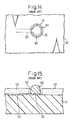
- circuit board As examples of such a circuit board as described above, there are a first circuit board shown in Figs. 14 to 16 and 17 to 19 and a second circuit board shown in Figs. 20 to 22.
- a circuit pattern 20 is formed on a surface of a substrate 10 thereof.
- a conductor pad 30 of a disc shape or other is formed on the circuit pattern 20.
- the substrate 10 is made of insulating material such as resin or ceramic.
- the circuit pattern 20 and the conductor pad 30 are formed by etching a copper foil adhered to the surface of the substrate 10 or by etching a metal skin applied to the surface of an insulating resin layer by a build-up system on the substrate 10.
- a resist layer 40 comprised of insulating resin or the like is broadly formed on the surface of the substrate 10 for the purpose of preventing solder from sticking to the surface of the substrate 10.
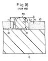
- the first circuit board shown in Figs. 14 to 16 has an opening 50 in the resist layer 40, in which are consecutively exposed the conductor pad 30, the circuit pattern 20 adjacent thereto and a surface of a portion of the substrate 10 therearound.
- the first circuit board shown in Figs. 17 to 19 has an opening 50 in the resist layer 40, in which is exposed a central portion of the conductor pad 30.
- a conductor bump 60 is formed on the conductor pad 30 exposed in the opening 50, which is of a semispherical shape and constituted by conductive resin plated with solder or Au or mixed with conductive filler.
- a metallized conductor pad 30 of a disc shape is provided on the surface of the substrate 10 made of ceramic or the like in the second circuit board.
- the conductor pad 30 is connected to the upper end of a column-like metallized conductor via 22 pierced through the substrate 10 in the thickness direction.
- the conductor via 22 constitutes a circuit pattern.
- a resist layer 40 formed of insulating resin or the like is broadly formed on the surface of the substrate 10 for the purpose of preventing solder from sticking thereto.
- a circular opening 50 is formed in the resist layer 40 so that a central portion of the conductor pad 30 is exposed therein.
- a conductor bump 60 is formed on the conductor pad 30 exposed in the opening 50 and is of a semispherical shape and is constituted by conductive resin plated with solder or Au or mixed with conductive filler.
- a height h1 from the surface of the resist layer 40 to a top of the conductor bump 60 is measured by means of an optical detector using a laser beam or a visible ray (hereinafter referred merely to a "photometer") or a CCD (which is an abridgement of Charge Coupled Device) camera. Then, based on this measured value, a height h2 from the surface of the substrate 10 to the top of the conductor bump 60 or a height h3 from the upper surface of the conductor pad 30 to the top of conductor bump 60 are estimated. Next, based on this estimated value, a variation of heights of the conductor bumps is determined. Finally, based on this variation, it is determined whether or not the above-mentioned first and second circuit boards are acceptable.
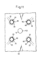
- the determination of whether or not the first and second circuit boards are acceptable is important because, if a large variation exists in height of the respective conductor bump 60 formed on the conductor pad 30 exposed in each of a plurality of openings 50 formed in the resist layer 40 in a matrix manner as shown in Figs. 23 and 24, there might be a risk in that when a plurality of conductor bumps 90 formed on electrodes arranged in correspondence to the conductor pads 30 on one side of a semiconductor chip 80 in a matrix manner are pressed onto the plurality of conductor bumps 60 at a predetermined pressure so that both the conductor bumps 60, 90 are at once welded or press-bonded together, all of the conductor bumps 60 and 90 may not be electrically connected to each other in a reliable manner.
- the resist layer 40 There are two methods for forming the resist layer 40; one method wherein a resist liquid is coated broadly on the surface of the substrate 10, which is then dried at a high temperature, and another method wherein a dry film of resist formed in a sheet form is adhered onto the surface of the substrate 10, which is then dried at a high temperature.
- the surface of the resist layer 40 formed broadly on the surface of the substrate 10 by these methods is not evenly flat but tends to undulate up and down, causing a variation in height everywhere on the surface of the resist layer 40.
- the variation f a height of the conductor bump 60 formed on the substrate 10 is correctly determined.
- the reason why the height h2 from the surface of the substrate 10 to the top of the conductor bump 60 could not be measured by the first method is that a gap between the conductor bump 60 and the inner wall of the opening 50 is too narrow as shown in Figs. 15 and 16, and therefore a width of the surface area of the substrate 10 exposed in the gap is also too small.
- the optical detector it is necessary to emit a laser beam or a visible ray from the optical detector disposed above the resist layer 40 onto the surface of the substrate 10 and reflect or diffuse the same to be directed to the optical detector.
- Such a reflected or diffused ray is difficult to make incident upon the optical detector due to the interference with the conductor bump 60 or the resist layer 40.
- a CCD camera is used to directly measure the height from the surface of the substrate 10 in the vicinity of the bump 60 exposed in the opening 50 to the top of the conductor bump 60 by the first method, it is also difficult to focus the CCD camera on the surface of the substrate 10 of a narrow width.
- the reason why the height h3 could not be measured by the second method is that the laser beam or a visible ray cannot pass through the conductor bump 60 to reach the upper surface of the conductor pad 30 beneath the former. Also, the laser beam or the visible ray reflected or diffused on the conductor pad 30 cannot pass through the conductor bump 60 to reach the optical detector or the CCD camera disposed above the resist layer 40.
- An object of the present invention is to provide a circuit board for mounting a semiconductor chip (hereinafter referred to as a circuit board) wherein the variation of heights of conductor bumps formed on a substrate for the circuit board can be directly, easily and reliably measured by an optical detector or a CCD camera.
- Another object of the present invention is to provide a circuit board for mounting a semiconductor chip which can solve the problems in the prior art mentioned above.
- a further object of the present invention is to provide a method for inspecting or measuring the circuit board, particularly the heights of conductor bumps of such a circuit board.
- a first circuit board wherein conductor pads to be electrically connected to electrodes of a semiconductor chip mounted to the substrate are formed on a circuit pattern provided on a surface of a substrate, and a resist layer made of insulating resin or the like is broadly formed on the surface of the substrate on which the circuit pattern and the conductor pads are provided, and wherein openings are formed in the resist layer so that the conductor pads are exposed therein, respectively, and the conductor bump is formed on the conductor pad exposed in the opening, characterized in that measurement holes are provided in the resist layer, in each of which is exposed a reference surface having a predetermined size or more necessary for measuring a height of the conductor bump by using an optical detector or a CCD camera.
- a second circuit board of the present invention wherein conductor pads to be electrically connected to electrodes of a semiconductor chip mounted to a substrate are formed on a surface of the substrate and of conductor pad is connected to an upper end of a conductor-via formed vertically through the substrate, and a resist layer made of insulating resin or the like is broadly formed on the surface of the substrate on which the conductor pads are provided, and wherein openings are formed in the resist layer so that the conductor pads are exposed therein, respectively, and the conductor bump is formed on the conductor pad exposed in the opening, characterized in that measurement holes are provided in the resist layer, in each of which is exposed a reference surface having a predetermined size or more necessary for measuring a height of the conductor bump by using an optical detector or a CCD camera.
- the measurement hole is broadly opened in the resist layer so that the reference surface having a predetermined size or more is exposed in the measurement hole.
- the optical detector disposed above the resist layer it is possible Lo direct a laser beam or a visible ray emitted from the optical detector disposed above the resist layer to the substrate through the broad measurement hole without interference from the resist layer.
- the laser beam or visible ray is projected onto the reference surface having the predetermined size or more exposed in the measurement hole and is reflected or diffused thereon.
- the reflected or diffused ray is incident upon the optical detector disposed above the resist layer through the broadly opened measurement hole.
- the laser beam or visible ray emitted from an optical detector disposed above the resist layer is incident upon a top of the conductor bump in the opening and reflects or diffuses thereon. Then, the reflected or diffused ray is incident upon the optical detector disposed above the resist layer.
- the height from the reference surface to the top of the conductor bump can be directly measured. Then, based on the measured value, it is possible to correctly determine the variation of the height of the conductor bump formed on the substrate.
- the reference surface is preferably defined by the substrate surface, the upper surface of the circuit pattern or the upper surface of the reference pattern provided on the substrate surface.
- the reference surface is preferably defined by the substrate surface or the upper surface of the reference pattern formed on the substrate surface.
- the first or second circuit board while defining a reference surface on the surface of the circuit pattern, the upper surface of the circuit pattern or the upper surface of the reference pattern, it is possible to directly measure the height h2 from the surface of the substrate to the top of the conductor bump, or to directly measure the height h4 from the upper surface of the circuit pattern to the top of the conductor bump, or to directly measure the height from the upper surface of the reference pattern to the top of the conductor bump. Based on the results of the measurements, the variation of the height of the conductor bump formed on the substrate is correctly determined.
- the circuit pattern defining the reference surface on its upper surface is formed to have the same thickness as the conductor pad, it is possible to correctly surmise that the height h3 from the upper surface of the conductor pad to the top of the conductor bump is the above-mentioned height h4. Based on this estimated value, the variation of the height of the conductor bump formed on the substrate can be correctly determined.
- the height h3 from the upper surface of the conductor pad to the top of the conductor bump can be correctly determined from the above-mentioned h4 while taking the difference in thickness between the circuit pattern and the conductor pad into account. Based on this estimated value, it is possible to correctly determine the variation of the height of the height of the conductor bump formed on the substrate.
- the measurement hole may be formed separately from the opening in the resist layer.
- the measurement hole may be preferably formed in the resist layer in continuous with the opening.
- the circuit board wherein the measurement hole is formed separately from the opening in the resist layer, it is possible to prevent part of the inner wall of the opening from being bored by the measurement hole.
- the conductor bump is formed on the conductor pad exposed in the opening, it is possible to prevent the conductor bump from bulging to the bored inner wall of the opening, and to obtain a generally semispherical shape of the conductor bump.
- the circuit board wherein the measurement hole is formed continuous with the opening in the resist layer it is possible to provide a measurement hole formed in an implement for coating a resist resin for forming the resist layer over the surface of the substrate, continuous with an opening provided in the implement. Thereby the implement for coating the resist resin can be simplified.
- a method for measuring a height of the conducting bump comprising: the following steps of:
- steps (1), (2) and (3) may either be step (1), step (2) and step (3), or step (2), step (1) and step (3).
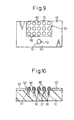
- Figs. 1, 2, 3 and 4 are partially enlarged plan views of preferred embodiments of a first circuit board according to the present invention, respectively.
- a square-shaped measurement hole 100 is provided in a resist layer 40 in each of the first circuit boards shown in Figs. 1 and 3 and the vicinity of an opening 50 but at a distance therefrom.
- a surface of a substrate 10 on which a circuit pattern 20 is formed is exposed within the measurement hole 100.
- a square-shaped measurement hole 102 is provided in a resist layer 40 in each of the first circuit boards shown in Figs. 2 and 4, in the vicinity of an opening 50 at a distance therefrom. A surface of a substrate 10 on which a circuit pattern 20 is not formed is exposed within the measurement hole 102.
- the measurement hole 100 or 102 has a predetermined open size or more so that the surface of the substrate 10 or the upper surface of the circuit pattern 20 defining a reference surface of a predetermined size or more is exposed within the measurement hole 100 or 102. Accordingly, a laser beam or a visible ray emitted from the above-mentioned optical detector (not shown) disposed above the resist layer 40 can be directed to the substrate 10 via the measurement hole 100 or 102, and reflected or diffused on the surface of the substrate 10 or the upper surface of the circuit pattern 20 exposed in the measurement hole 100 or 102. The reflected or diffused ray is incident upon the optical detector through the measurement hole 100 or 102 without interference from the resist layer 40 around the measurement hole 100 or 102.
- the CCD camera disposed above the resist layer 40 can be easily and correctly focussed on the surface of the substrate 100 or the upper surface of the circuit pattern 20 of the predetermined size or more exposed in the measurement hole 100 or 102 without interference from the resist layer 40 around the measurement hole 100 or 102.
- Each of the first circuit boards shown in Figs. 1, 2, 3 and 4 has the same structure, other than above, as that of the first circuit board described with reference to Figs. 14 to 16 or 17 to 19, whereby it is possible to project the reflected or diffused ray upon the optical detector disposed above the resist layer 40.
- the height h2 can be directly measured by the optical detector. Then, based on the measured value, the variation of the height of the conductor bump 60 can be correctly determined.
- the height h2 is directly measurable. Thereafter, the height variation of the conductor bumps 60 can be correctly determined from the measured values.
- the height h4 from the upper surface of the circuit pattern 20 defining the reference surface to the top of the conductor bump 60 is directly measurable.
- the circuit pattern 20 is formed to have the same thickness as the conductor pad 30, it is apparent that the height h3 from the upper surface of the conductor pad 30 to the top of the conductor bump 60 is correctly the same as the above-mentioned height h4. Based on this estimated value, it is possible to correctly determine the variation of the height of the top of the conductor bump 60 formed on the substrate 10.
- circuit pattern 20 is formed to have a different thickness from the conductor pad 30, it is possible to correctly estimate the height h3 from the upper surface of the conductor pad 30 to the top of the conductor bump 60 while taking the difference in thickness between the circuit pattern 20 and the conductor pad 30 into account. Based on this estimated value, it is possible to correctly determine the variation of the height of the conductor bump 60 formed on the substrate 10.
- Figs. 5 and 6 are partially enlarged plan views, respectively, of other preferable embodiments of a first circuit board of the present invention.
- an elongate measurement hole 104 extending outward from the opening 50 is formed in the resist layer 40.
- an elongate measurement hole 106, of a strip form, extending between two adjacent openings 50 is formed in the resist layer 40.
- Each of the measurement holes 104 and 106 has a predetermined size or more whereby a surface of the substrate 10 defining a reference surface of a predetermined size or more is exposed in the measurement hole 104, 106.
- a laser beam or a visible ray emitted from the optical detector (not shown) disposed above the resist layer 40 is directed to the surface of the substrate 10 exposed in the measurement hole 104 or 106 through the measurement hole 104 or 106 without interference from the resist layer 40 therearound is and reflected or diffused on the substrate surface.
- the CCD camera disposed above the resist layer 40 is easily and properly focussed on the surface of the substrate 10 having the predetermined size or more and defining the reference surface exposed in the measurement holes 104 or 106, without interference from the resist layer 40 around the measurement hole 104 or 106.
- the remainder of the circuit board other than described above is the same as that described with reference to Figs. 14 to 16.
- the measurement hole 104 or 106 formed in the resist layer 40 may be provided to be continuous to the opening 50 also formed in the resist layer 40.
- a tool for forming the measurement hole 104 or 106 and the opening 50 can be simplified and the process for forming the measurement hole 104 or 106 and the opening 50 becomes easy. Operations other than the above are the same as those of the first circuit board described with reference to Fig. 2.
- Figs. 7 and 8 are partially enlarged plan views, respectively, of other preferable embodiments of a second circuit board of the present invention.
- a measurement hole 108 of a circular shape or the like is provided in the resist layer 40 in the vicinity of the opening 50 but separate therefrom.
- the surface of the substrate 10 defining the reference surface is exposed in the measurement hole 108.
- an elongate measurement hole 110 is provided in the resist layer 40 in the vicinity of the opening 50, while extending outward therefrom.
- the surface of the substrate 10 defining the reference surface is exposed in the measurement hole 110.
- Each of the measurement holes 108 and 110 has a predetermined size or more so that the surface of the substrate 10 defining the reference surface having a predetermined size or more is exposed in the measurement hole 108 or 110.
- a laser beam or a visible ray emitted from the optical detector disposed above the resist layer 40 as described before is directed to the substrate 10 through the measurement hole 108 or 110 and reflects or diffuses on the surface of the substrate 10 exposed in the measurement hole 108 or 110.
- the reflected or diffused ray can be incident upon the optical detector through the measurement hole 108 or 110 without interference from the resist layer 40 around the measurement hole 108 or 110.
- circuit board other than described above is the same as that described with reference to Figs. 20 to 22.
- the second circuit board shown in Fig. 7 or 8 it is possible to direct a laser beam or a visible ray emitted from the optical detector disposed above the resist layer 40 to the substrate 10 through the widely opened measurement hole 108 or 110 without the interference with the resist layer 40 and it is possible to reflect or diffuse the laser beam or the visible ray on the surface of the substrate 10 having the predetermined size exposed in the measurement hole 108 or 110.
- the reflected or diffused ray is incident upon the optical detector disposed above the resist layer 40 through the widely opened measurement hole 108 or 110 without interference from the resist layer.
- the laser beam or the visible ray emitted from the optical detector disposed above the resist layer 40 it is possible to cause the laser beam or the visible ray emitted from the optical detector disposed above the resist layer 40 to be incident upon the top of the conductor bump 60 in the opening 50 and reflect or diffuse the same on the top of the bump 60.
- the reflected or diffused ray is incident upon the optical detector disposed above the resist layer 40.
- the reflected or diffused ray reflected or diffused on the surface of the substrate 10 and incident upon the optical detector and the reflected or diffused ray reflected or diffused on the top of the conductor bump 60 are used to directly measure the height h2 from the surface of the substrate 10 defining the reference surface to the top of the conductor bump 60. Based on the measured value, it is possible to correctly determine the variation of the height of the conductor bump 60 formed on the substrate 10.
- a CCD camera disposed above the resist layer 40 can be focussed on the top of the conductor bump 60 exposed in the conductor bump 60, and a distance from the CCD camera to the top of the conductor bump 60 is measurable by the CCD camera.
Landscapes
- Engineering & Computer Science (AREA)
- Manufacturing & Machinery (AREA)
- Microelectronics & Electronic Packaging (AREA)
- Length Measuring Devices By Optical Means (AREA)
- Testing Or Measuring Of Semiconductors Or The Like (AREA)
- Non-Metallic Protective Coatings For Printed Circuits (AREA)
- Electric Connection Of Electric Components To Printed Circuits (AREA)
Applications Claiming Priority (2)
| Application Number | Priority Date | Filing Date | Title |
|---|---|---|---|
| JP20999298 | 1998-07-24 | ||
| JP10209992A JP2000040867A (ja) | 1998-07-24 | 1998-07-24 | 半導体チップ実装用回路基板 |
Publications (2)
| Publication Number | Publication Date |
|---|---|
| EP0975019A2 true EP0975019A2 (fr) | 2000-01-26 |
| EP0975019A3 EP0975019A3 (fr) | 2000-11-29 |
Family
ID=16582074
Family Applications (1)
| Application Number | Title | Priority Date | Filing Date |
|---|---|---|---|
| EP99305831A Withdrawn EP0975019A3 (fr) | 1998-07-24 | 1999-07-22 | Circuit imprimé pour de puces et methode de mesure le meme |
Country Status (4)
| Country | Link |
|---|---|
| US (1) | US6259038B1 (fr) |
| EP (1) | EP0975019A3 (fr) |
| JP (1) | JP2000040867A (fr) |
| KR (1) | KR20000011897A (fr) |
Families Citing this family (21)
| Publication number | Priority date | Publication date | Assignee | Title |
|---|---|---|---|---|
| KR100546695B1 (ko) * | 2000-08-24 | 2006-01-26 | 앰코 테크놀로지 코리아 주식회사 | 반도체 패키지 제조용 가요성 필름 구조 |
| US6583019B2 (en) * | 2001-11-19 | 2003-06-24 | Gennum Corporation | Perimeter anchored thick film pad |
| SG121707A1 (en) * | 2002-03-04 | 2006-05-26 | Micron Technology Inc | Method and apparatus for flip-chip packaging providing testing capability |
| TWI234258B (en) * | 2003-08-01 | 2005-06-11 | Advanced Semiconductor Eng | Substrate with reinforced structure of contact pad |
| IL180149A (en) * | 2006-12-18 | 2012-06-28 | David Eduar Sitbon | Method of advertising by using computer multi-monitor monitors |
| JP4303282B2 (ja) * | 2006-12-22 | 2009-07-29 | Tdk株式会社 | プリント配線板の配線構造及びその形成方法 |
| IL180477A (en) * | 2007-01-01 | 2013-05-30 | David Eduar Sitbon | A system and method for proofreading and digital and multilateral repair within a meeting |
| TWI357647B (en) * | 2007-02-01 | 2012-02-01 | Siliconware Precision Industries Co Ltd | Semiconductor substrate structure |
| JP2008205244A (ja) * | 2007-02-21 | 2008-09-04 | Sony Chemical & Information Device Corp | プリント配線板及びプリント配線板の製造方法 |
| JP4331769B2 (ja) * | 2007-02-28 | 2009-09-16 | Tdk株式会社 | 配線構造及びその形成方法並びにプリント配線板 |
| CN101336042B (zh) * | 2007-06-29 | 2012-05-16 | 鸿富锦精密工业(深圳)有限公司 | 焊盘、具有该焊盘的电路板和电子装置 |
| CN101568224B (zh) * | 2008-04-22 | 2012-01-25 | 鸿富锦精密工业(深圳)有限公司 | 电路板及具有该电路板的电子装置 |
| US7932170B1 (en) * | 2008-06-23 | 2011-04-26 | Amkor Technology, Inc. | Flip chip bump structure and fabrication method |
| CN101730398A (zh) * | 2008-10-23 | 2010-06-09 | 鸿富锦精密工业(深圳)有限公司 | 印刷电路板及其制作方法 |
| TWI549577B (zh) * | 2012-11-22 | 2016-09-11 | 鴻海精密工業股份有限公司 | 光纖連接器電路基板及光纖連接器 |
| WO2016097817A1 (fr) * | 2014-12-15 | 2016-06-23 | Assa Abloy Ab | Procédé de production d'incrustation fonctionnelle et incrustation produite au moyen du procédé |
| KR101495323B1 (ko) * | 2014-12-29 | 2015-02-24 | 아메스산업(주) | 벤트홀을 이용한 플립칩 얼라인먼트 검사 장치 및 방법 |
| JP6659253B2 (ja) * | 2015-06-24 | 2020-03-04 | 住友電工プリントサーキット株式会社 | フレキシブルプリント配線板及びフレキシブルプリント配線板の製造方法 |
| JP7213876B2 (ja) * | 2018-06-29 | 2023-01-27 | 株式会社荏原製作所 | バンプ高さ測定装置、基板処理装置、バンプ高さ測定方法、記憶媒体 |
| JP2020134407A (ja) | 2019-02-22 | 2020-08-31 | キオクシア株式会社 | 検査装置および検査方法 |
| KR102783279B1 (ko) * | 2020-07-07 | 2025-03-20 | 삼성디스플레이 주식회사 | 표시 패널 및 이의 제조 방법 |
Family Cites Families (16)
| Publication number | Priority date | Publication date | Assignee | Title |
|---|---|---|---|---|
| DE531984C (de) * | 1929-11-07 | 1931-08-20 | Hazel Atlas Glass Company | Verfahren und Vorrichtung zum absatzweisen Eintragen des Gemenges in Glasschmelzoefen |
| JP2557960B2 (ja) | 1988-09-19 | 1996-11-27 | 株式会社日立製作所 | 高さ測定方法 |
| JPH0479261A (ja) | 1990-07-20 | 1992-03-12 | Matsushita Electric Works Ltd | ピングリッドアレイ用プリント配線板 |
| JP2678958B2 (ja) * | 1992-03-02 | 1997-11-19 | カシオ計算機株式会社 | フィルム配線基板およびその製造方法 |
| US5489750A (en) * | 1993-03-11 | 1996-02-06 | Matsushita Electric Industrial Co., Ltd. | Method of mounting an electronic part with bumps on a circuit board |
| US5465152A (en) | 1994-06-03 | 1995-11-07 | Robotic Vision Systems, Inc. | Method for coplanarity inspection of package or substrate warpage for ball grid arrays, column arrays, and similar structures |
| JPH08327327A (ja) | 1995-06-02 | 1996-12-13 | Tokyo Seimitsu Co Ltd | バンプ高さ測定方法及び装置 |
| JP3330468B2 (ja) * | 1995-06-30 | 2002-09-30 | 富士通株式会社 | 配線基板及び半導体装置 |
| KR100192766B1 (ko) * | 1995-07-05 | 1999-06-15 | 황인길 | 솔더볼을 입출력 단자로 사용하는 볼그리드 어레이 반도체 패키지의 솔더볼 평탄화 방법 및 그 기판구조 |
| JP3335826B2 (ja) | 1995-12-05 | 2002-10-21 | 株式会社日立製作所 | はんだバンプの測定装置 |
| US5973931A (en) * | 1996-03-29 | 1999-10-26 | Sony Corporation | Printed wiring board and electronic device using same |
| US5738269A (en) | 1996-04-19 | 1998-04-14 | Motorola, Inc. | Method for forming a solder bump |
| JP3593833B2 (ja) * | 1997-02-10 | 2004-11-24 | 富士通株式会社 | 半導体装置 |
| US5847936A (en) * | 1997-06-20 | 1998-12-08 | Sun Microsystems, Inc. | Optimized routing scheme for an integrated circuit/printed circuit board |
| JPH1154884A (ja) * | 1997-08-06 | 1999-02-26 | Nec Corp | 半導体装置の実装構造 |
| JPH1187896A (ja) * | 1997-09-10 | 1999-03-30 | Canon Inc | プリント配線板 |
-
1998
- 1998-07-24 JP JP10209992A patent/JP2000040867A/ja active Pending
-
1999
- 1999-07-21 US US09/358,053 patent/US6259038B1/en not_active Expired - Fee Related
- 1999-07-22 KR KR1019990029769A patent/KR20000011897A/ko not_active Withdrawn
- 1999-07-22 EP EP99305831A patent/EP0975019A3/fr not_active Withdrawn
Also Published As
| Publication number | Publication date |
|---|---|
| EP0975019A3 (fr) | 2000-11-29 |
| KR20000011897A (ko) | 2000-02-25 |
| US6259038B1 (en) | 2001-07-10 |
| JP2000040867A (ja) | 2000-02-08 |
Similar Documents
| Publication | Publication Date | Title |
|---|---|---|
| US6259038B1 (en) | Semiconductor chip mounting board and method of inspecting the same mounting board | |
| US5828128A (en) | Semiconductor device having a bump which is inspected from outside and a circuit board used with such a semiconductor device | |
| US5914536A (en) | Semiconductor device and soldering portion inspecting method therefor | |
| US5465152A (en) | Method for coplanarity inspection of package or substrate warpage for ball grid arrays, column arrays, and similar structures | |
| US6580036B2 (en) | Multi-layer printed circuit board and a BGA semiconductor package using the multi-layer printed circuit board | |
| US6428202B1 (en) | Method for inspecting connection state of electronic part and a substrate, and apparatus for the same | |
| US7888958B2 (en) | Current test probe having a solder guide portion, and related probe assembly and production method | |
| KR20000035210A (ko) | 반도체 장치, 반도체 장치용 접속용 기판, 및 접속용기판의 제조 방법 | |
| US6546622B2 (en) | Printed-wiring substrate and method for fabricating the same | |
| US5734475A (en) | Process of measuring coplanarity of circuit pads and/or grid arrays | |
| US20020096750A1 (en) | Package for semiconductor chip having thin recess portion and thick plane portion | |
| JP3601714B2 (ja) | 半導体装置及び配線基板 | |
| JPH02198186A (ja) | プリント配線板シールド層検査方法と検査手段 | |
| JP3635882B2 (ja) | 電子部品実装基板 | |
| JPH05283825A (ja) | 認識マーク付きプリント基板 | |
| JP2764637B2 (ja) | 電子部品搭載用基板 | |
| TWI227548B (en) | Testing method for high density flip chip BGA | |
| JPH09283921A (ja) | プリント基板及びプリント基板に印刷した半田の膜厚測定方法 | |
| JP3301647B2 (ja) | 塗布検査装置 | |
| JPH0964495A (ja) | 位置認識マーク付配線基板および配線基板の位置認識方法 | |
| JPH04186731A (ja) | 回路部品搭載用端子を備えた回路基板及びその製造法 | |
| JPH05315519A (ja) | 半導体素子 | |
| JPH11251740A (ja) | プリント基板およびその製造方法 | |
| JP2003232811A (ja) | 検査用プローブ基板及びその製造方法 | |
| JPH04178507A (ja) | 半田の外観検査方法 |
Legal Events
| Date | Code | Title | Description |
|---|---|---|---|
| PUAI | Public reference made under article 153(3) epc to a published international application that has entered the european phase |
Free format text: ORIGINAL CODE: 0009012 |
|
| AK | Designated contracting states |
Kind code of ref document: A2 Designated state(s): DE FR GB |
|
| AX | Request for extension of the european patent |
Free format text: AL;LT;LV;MK;RO;SI |
|
| PUAL | Search report despatched |
Free format text: ORIGINAL CODE: 0009013 |
|
| AK | Designated contracting states |
Kind code of ref document: A3 Designated state(s): AT BE CH CY DE DK ES FI FR GB GR IE IT LI LU MC NL PT SE |
|
| AX | Request for extension of the european patent |
Free format text: AL;LT;LV;MK;RO;SI |
|
| RIC1 | Information provided on ipc code assigned before grant |
Free format text: 7H 01L 21/66 A, 7H 01L 21/60 B |
|
| 17P | Request for examination filed |
Effective date: 20010515 |
|
| AKX | Designation fees paid |
Free format text: DE FR GB |
|
| 17Q | First examination report despatched |
Effective date: 20071122 |
|
| STAA | Information on the status of an ep patent application or granted ep patent |
Free format text: STATUS: THE APPLICATION IS DEEMED TO BE WITHDRAWN |
|
| 18D | Application deemed to be withdrawn |
Effective date: 20080403 |