EP0977250A2 - Anordnung und Verfahren zur Herstellung eines Heterobipolartransistors - Google Patents
Anordnung und Verfahren zur Herstellung eines Heterobipolartransistors Download PDFInfo
- Publication number
- EP0977250A2 EP0977250A2 EP99114471A EP99114471A EP0977250A2 EP 0977250 A2 EP0977250 A2 EP 0977250A2 EP 99114471 A EP99114471 A EP 99114471A EP 99114471 A EP99114471 A EP 99114471A EP 0977250 A2 EP0977250 A2 EP 0977250A2
- Authority
- EP
- European Patent Office
- Prior art keywords
- layer
- base
- emitter
- ingaas
- collector
- Prior art date
- Legal status (The legal status is an assumption and is not a legal conclusion. Google has not performed a legal analysis and makes no representation as to the accuracy of the status listed.)
- Withdrawn
Links
Images


Classifications
-
- H—ELECTRICITY
- H10—SEMICONDUCTOR DEVICES; ELECTRIC SOLID-STATE DEVICES NOT OTHERWISE PROVIDED FOR
- H10D—INORGANIC ELECTRIC SEMICONDUCTOR DEVICES
- H10D10/00—Bipolar junction transistors [BJT]
- H10D10/01—Manufacture or treatment
- H10D10/021—Manufacture or treatment of heterojunction BJTs [HBT]
-
- H—ELECTRICITY
- H10—SEMICONDUCTOR DEVICES; ELECTRIC SOLID-STATE DEVICES NOT OTHERWISE PROVIDED FOR
- H10D—INORGANIC ELECTRIC SEMICONDUCTOR DEVICES
- H10D10/00—Bipolar junction transistors [BJT]
- H10D10/80—Heterojunction BJTs
- H10D10/821—Vertical heterojunction BJTs
-
- H—ELECTRICITY
- H10—SEMICONDUCTOR DEVICES; ELECTRIC SOLID-STATE DEVICES NOT OTHERWISE PROVIDED FOR
- H10D—INORGANIC ELECTRIC SEMICONDUCTOR DEVICES
- H10D62/00—Semiconductor bodies, or regions thereof, of devices having potential barriers
- H10D62/80—Semiconductor bodies, or regions thereof, of devices having potential barriers characterised by the materials
- H10D62/85—Semiconductor bodies, or regions thereof, of devices having potential barriers characterised by the materials being Group III-V materials, e.g. GaAs
Definitions
- the invention relates to a method for producing a Heterobipolar transistor according to the preamble of claim 1 and an arrangement of a heterobipolar transistor according to the preamble of Claim 4.
- High-frequency circuits such as power amplifiers, oscillators or mixers.
- An increase in the limit frequencies f T and f max of transistors is an important prerequisite for technical innovations in mobile or short-range communication systems and phase-controlled antennas.
- transistors from Shigematsu, H. et al .; IEEE Electron Device Letters, Vol. 16, No. 2, pp. 55-57, (1995) known the Manufacturing process of an InP / InGaAs heterobipolar transistor in connection with a polyimide planarization process for basic contacting for one Use at high frequencies describes.
- the component production is by means of a self-adjustment process sequence on a complex so-called dummy emitter structure and spacers performed. The simplest possible would be desirable and in the process sequence reliable manufacturing method with the parasitic Lower capacities.
- the invention has for its object to provide a method and an arrangement with which an optimization of the high-frequency properties of a heterobipolar transistor is achieved by minimizing the parasitic base-collector capacitance in order to bring about an increase in the cut-off frequencies f T and f max .
- the invention is related to the method by the features of Claim 1 and in relation to the arrangement of a Heterobipolar transistor by the features of claim 4 reproduced.
- the other claims contain advantageous training and Developments of the invention.
- the invention includes a two-stage process for planarizing a semiconductor surface with polyimide, in which, compared to the prior art, potential damage to the extrinsic region of the base is prevented.
- the process sequence includes growing a layer sequence on a substrate made of semiconductor material, in which layers for a collector, a base and an emitter are deposited one above the other.
- the transistor is then structured in a mesa design.
- a first planarization step is then carried out up to the base mesa, with a remainder of the subsequent emitter layer protecting the surface of the base during this first planarization step.
- This protective layer is then removed, for example by low-damage wet chemical etching, and the metallization of the base is applied.
- the base mesa is dimensioned extremely narrow, so that the base metal extends laterally onto the first planarization layer and, in particular, a metal conductor track is led over the planarization layer for contacting.
- a flat semiconductor surface is generated by a second planarization step up to the emitter mesa.
- the emitter metallization 5 which is preferably composed of the metal layer sequence Ti / Pt / Au.
- the second n + emitter cap layer 43 made of InGaAs is then etched away, the preceding emitter metallization 5 serving as a self-adjusting etching mask.
- the InP n emitter layer 41 and the first n + emitter cap layer 42 made of InP initially remain as protective layers over the InGaAs base 31 and 32 over the entire area.
- the production of an extraordinarily narrow base collector mesa 12 (FIG. 9), which extends into the n + sub collector layer 21, is carried out with a photoresist mask.
- a chemically assisted ion beam etching method (CAIBE) is selected for the InP layers 41 and 42, in which a process gas mixture Cl 2 / Ar is used for the removal.
- the InGaAs layers 21, 22, 31 and 32 are removed wet-chemically with a phosphoric acid-hydrogen-peroxide mixture (H 3 PO 4 : H 2 O 2 : H 2 O).
- the subsequent production of a collector-substrate mesa 13, which extends into the substrate 1, serves to isolate the component.
- the collector metal 6 is applied using a photoresist mask.
- a first planarization step is then carried out, in which the semiconductor surface is covered up to the upper limit of the base.
- a first polyimide layer 7 is applied, which is etched back in the oxygen plasma up to the upper limit of the base by means of a reactive ion etching process (RIE).
- RIE reactive ion etching process
- the InP protective layer 41 and 42 is of central importance for the etching back of the polyimide layer 7.
- the InP n emitter layer 41 and the first n + emitter cap layer 42 made of InP are then removed using an etching solution based on hydrochloric acid, and the base metal 8 is applied to the emitter base mesa 11 in a self-adjusting manner immediately thereafter.
- the base metal 8 extends laterally onto the first planarization layer, this in particular being continued as a metal conductor track for making contact via the first polyimide layer 7.
- a second planarization step the semiconductor surface is covered up to the upper limit of the emitter.
- a second polyimide layer 9 is again applied, which is etched back in the oxygen plasma up to the upper limit of the emitter.
- the last process document contains the connection metallization 10 of emitter 4, base 3 and collector 2 by means of reactive ion etching and an electrochemical deposition of gold in the areas provided for this.
- the semiconductor layer sequence can be varied on the basis of the process sequence used according to exemplary embodiment 1.
- the InGaAs intrinsic base spacer layer 32 and / or the first n + emitter cap layer 42 made of InP can also be dispensed with.
- the n-emitter layer 41 and the first n + -emitter cap layer 42 can also consist of InAlAs.
- a second n + emitter cap layer 43 made of InGaAs with a thickness of 20 nm and a doping concentration of approx. 1x10 19 cm -3 can follow on the first n + emitter cap layer 42, the In content in the layer having a gradient between 0% up to 50%.
- an AlGaAs n layer with a gradient in the Al content between 30% to 0% can be used, with a thickness of 30 nm and the doping concentration of approx. 1x10 18 cm -3 .
Landscapes
- Bipolar Transistors (AREA)
Abstract
Description
Der Transistor wird anschließend in Mesabauweise strukturiert.
Danach wird ein erster Planarisierungsschritt bis zur Basis-Mesa durchgeführt, wobei während diesem ersten Planarisierungsschritt ein Rest der darauffolgenden Emitterschicht die Oberfläche der Basis schützt. Anschließend wird diese Schutzschicht beispielsweise durch eine schädigungsarme naßchemische Ätzung abgetragen und die Metallisierung der Basis aufgebracht. Die Basis-Mesa ist außerordentlich schmal dimensioniert, so daß sich das Basismetall lateral auf die erste Planarisierungsschicht ausdehnt und insbesondere eine Metalleiterbahn zur Anschlußkontaktierung über die Planarisierungsschicht geführt wird. Eine ebene Halbleiteroberfläche wird durch einen zweiten Planarisierungsschritt bis über die Emitter-Mesa erzeugt.
Ein weiterer Vorteil bei der Planarisierung ergibt sich aus den technologisch gut kontrollierbaren Einzelschritten der Prozeßfolge, wobei die Materialauswahl beispielsweise nicht auf InP beschränkt ist, sondern auch für andere Halbleiterschichtenfolgen anwendbar ist.
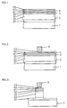
Im folgenden wird die Erfindung anhand von vorteilhaften Ausführungsbeispielen unter Bezugnahme auf schematische Zeichnungen in den Figuren näher erläutert. Es zeigen:
- Fig. 1
- Schichtenfolge des Heterobipolartransistors,
- Fig. 2
- Selbstjustage des Emitters,
- Fig. 3
- Herstellung der Basis-Kollektor-Mesa,
- Fig. 4
- Mesabauweise des Transistors,
- Fig. 5
- erster Planarisierungsschritt bis zur Basis-Mesa mit Rest der auf die Basis folgenden Emitterschicht,
- Fig. 6
- Metallisierung der Basis,
- Fig. 7
- zweiter Planarisierungsschritt über die Emitter-Basis-Mesa,
- Fig. 8
- Kontaktieren von Emitter, Basis und Kollektor,.
- Fig. 9
- Transistoraufbau mit Mesastruktur in Projektion.
- einer InGaAs n+-Subkollektorschicht 21 einer Dicke von 600 nm und der Dotierkonzentration von ca. 1x1019 cm-3,
- einer InGaAs n-Kollektorschicht 22 einer Dicke von 500 nm und der Dotierkonzentration von ca. 1x1016 cm-3,
- einer InGaAs p+-Basisschicht 31 einer Dicke von 90 nm und der Be- oder C-Dotierkonzentration von ca. 4x1019 cm-3,
- einer InGaAs intrinsischen Basisspacerschicht 32 einer Dicke von 7 nm,
- einer InP n-Emitterschicht 41 einer Dicke von 60 nm und der Dotierkonzentration von ca. 3x1017 cm-3,
- einer ersten n+-Emittercapschicht 42 aus InP einer Dicke von 50 nm und der Dotierkonzentration von ca. 1x1019 cm-3,
- einer zweiten n+-Emittercapschicht 43 aus InGaAs einer Dicke von 180 nm und der Dotierkonzentration von ca. 1x1019 cm-3.
Anschließend wird ein erster Planarisierungsschritt durchgeführt, bei dem die Halbleiteroberfläche bis zur Obergrenze der Basis abgedeckt wird. Hierzu wird eine erste Polyimidschicht 7 aufgebracht, die mittels eines reaktiven Ionenätzverfahrens (RIE) im Sauerstoffplasma bis zur Obergrenze der Basis zurückgeätzt wird. Die InP Schutzschicht 41 und 42 ist für das Rückätzen der Polyimidschicht 7 von zentraler Bedeutung. Danach wird die InP n-Emitterschicht 41 und erste n+-Emittercapschicht 42 aus InP mit einer auf Salzsäure basierenden Ätzlösung abgetragen und unmittelbar danach das Basismetall 8 selbstjustierend gegenüber der Emitter-Basis-Mesa 11 aufgebracht. Dabei erstreckt sich das Basismetall 8 lateral auf die erste Planarisierungsschicht, wobei insbesondere diese als Metalleiterbahn zur Anschlußkontaktierung über die erste Polyimidschicht 7 weitergeführt wird.
Eine Verbesserung der Hochfrequenz-Eigenschaften eines Transistors durch eine Verringerung der parasitären Basis-Kollektor-Kapazität CBC um bis zu 56% und infolge dessen eine beträchtliche Steigerung der Grenzfrequenzen fT und fmax um bis zu 35% wurden beobachtet.
In einem zweiten Ausführungsbeispiel können, unter Zugrundelegen der nach Ausführungsbeispiel 1 verwendeten Prozeßfolge, die Halbleiterschichtenfolge variiert werden. Beispielsweise kann auch auf die InGaAs intrinsische Basisspacerschicht 32 und/oder die erste n+-Emittercapschicht 42 aus InP verzichtet werden. Weiterhin können die n-Emitterschicht 41 und die erste n+-Emittercapschicht 42 auch aus InAlAs bestehen.
- einer GaAs n+-Subkollektorschicht 21 einer Dicke von 600 nm und der Dotierkonzentration von ca. 5x1018 cm-3,
- einer GaAs n-Kollektorschicht 22 einer Dicke von 500 nm und der Dotierkonzentration von ca. 1x1016 cm-3,
- einer GaAs p+-Basisschicht 31 einer Dicke von 90 nm und der Be- oder C-Dotierkonzentration von ca. 4x1019 cm-3
- einer GaAs intrinsischen Basisspacerschicht 32 einer Dicke von 7 nm,
- einer AlGaAs n-Emitterschicht 41, mit einem Al-Gehalt zwischen 25%-35%, einer Dicke von 60 nm und der Dotierkonzentration von ca. 3x1017 cm-3,
- einer ersten n+-Emittercapschicht 42 aus GaAs einer Dicke von 200 nm und der Dotierkonzentration von ca. 5x1018 cm-3.
Claims (11)
- Verfahren zur Herstellung eines aufeinem Substrat (1) aus Halbleitermaterial angeordneten Heterobipolartransistors, bei dem eine Halbleiterschichtenfolge für einen Kollektor (2), eine Basis (3) und einem Emitter (4) aufgewachsen wird, dadurch gekennzeichnet,daß der Transistor in Mesabauweise strukturiert wird,daß ein erster Planarisierungsschritt bis zur Obergrenze der Basis (3) durchgeführt wird, wobei während diesem ersten Planarisierungsschritt die Oberfläche der Basis durch eine Schutzschicht (41, 42) der aufdie Basis folgenden Emitterschicht geschützt wird,daß diese Schutzschicht (41, 42) abgetragen und ein Basismetall (8) aufgebracht wird,daß ein zweiter Planarisierungsschritt über die Basis-Emitter-Mesa (11) erfolg, unddaß eine Anschlußmetallisierung (10) aufgebracht wird.
- Verfahren nach Anspruch 1, dadurch gekennzeichnet, daß beim ersten und zweiten Planarisierungsschritt Polyimidschichten (7, 9) verwendet werden.
- Verfahren nach Anspruch 1, dadurch gekennzeichnet, daß das Basismetall (8) lateral über die Basis-Kollektor-Mesa (12) hinaus auf auf Bereiche der ersten Planarisierungsschicht (7) abgeschieden wird.
- Heterobipolartransistor, hergestellt nach einem der Ansprüche 1 bis 3, dadurch gekennzeichnet, daß die Halbleiterschichtenfolge auseiner InGaAs n+-Subkollektorschicht (21),einer InGaAs n-Kollektorschicht (22),einer InGaAs p+-Basisschicht (31),einer InGaAs intrinsischen Basisspacerschicht (32),einer InP n-Emitterschicht (41),einer ersten n+-Emittercapschicht (42) aus InP,einer zweiten n+-Emittercapschicht (43) aus InGaAs auf dem Substrat (1) aus halbisolierendem InP besteht.
- Heterobipolartransistor nach Anspruch 4, dadurch gekennzeichnet, daß die Schutzschicht aus der InP n-Emitterschicht (41) und der ersten n+-Emittercapschicht (42) aus InP besteht.
- Heterobipolartransistor, hergestellt nach einem der Ansprüche 1 bis 3, dadurch gekennzeichnet, daß die Halbleiterschichtenfolge auseiner InGaAs n+-Subkollektorschicht (21),einer InGaAs n-Kollektorschicht (22),einer InGaAs p+-Basisschicht (31),einer InGaAs intrinsischen Basisspacerschicht (32),einer InP n-Emitterschicht (41),einer zweiten n+-Emittercapschicht (43) aus InGaAs aufdem Substrat (1) aus halbisolierendem InP besteht.
- Heterobipolartransistor nach Anspruch 6, dadurch gekennzeichnet, daß die Schutzschicht aus der InP n-Emitterschicht (41) besteht.
- Heterobipolartransistor, hergestellt nach einem der Ansprüche 1 bis 3, dadurch gekennzeichnet, daß die Halbleiterschichtenfolge auseiner GaAs n+-Subkollektorschicht (21),einer GaAs n-Kollektorschicht (22),einer GaAs p+-Basisschicht (31),einer GaAs intrinsischen Basisspacerschicht (32),einer AlGaAs n-Emitterschicht (41),einer ersten n+-Emittercapschicht (42) aus GaAs, auf dem Substrat (1) aus halbisolierendem GaAs besteht.
- Heterobipolartransistor nach Anspruch 8, dadurch gekennzeichnet, daß auf der ersten n+-Emittercapschicht (42) eine zweite n+-Emittercapschicht (43) aus InGaAs folgt, wobei der In-Gehalt in der Schicht einen Gradienten zwischen 0 % bis 50 % aufweist.
- Heterobipolartransistor nach Anspruch 8 oder 9, dadurch gekennzeichnet, daß zwischen der n-Emitterschicht (41) und der ersten n+-Emittercapschicht (42) eine AlGaAs n-Schicht, mit einen Gradienten im Al-Gehalt zwischen 30 % bis 0 % angeordnet ist.
- Heterobipolartransistor, hergestellt nach einem der Ansprüche 1 bis 3, dadurch gekennzeichnet, daß das Basismetall (8) lateral über die Basis-Kollektor-Mesa (12) hinaus auf Bereiche der ersten Planarisierungsschicht (7) erstreckt.
Applications Claiming Priority (2)
| Application Number | Priority Date | Filing Date | Title |
|---|---|---|---|
| DE19834491 | 1998-07-31 | ||
| DE19834491A DE19834491A1 (de) | 1998-07-31 | 1998-07-31 | Anordnung und Verfahren zur Herstellung eines Heterobipolartransistors |
Publications (2)
| Publication Number | Publication Date |
|---|---|
| EP0977250A2 true EP0977250A2 (de) | 2000-02-02 |
| EP0977250A3 EP0977250A3 (de) | 2000-03-22 |
Family
ID=7875930
Family Applications (1)
| Application Number | Title | Priority Date | Filing Date |
|---|---|---|---|
| EP99114471A Withdrawn EP0977250A3 (de) | 1998-07-31 | 1999-07-23 | Anordnung und Verfahren zur Herstellung eines Heterobipolartransistors |
Country Status (4)
| Country | Link |
|---|---|
| US (1) | US6365477B1 (de) |
| EP (1) | EP0977250A3 (de) |
| JP (1) | JP2000058557A (de) |
| DE (1) | DE19834491A1 (de) |
Cited By (3)
| Publication number | Priority date | Publication date | Assignee | Title |
|---|---|---|---|---|
| WO2002103802A3 (en) * | 2001-06-18 | 2003-02-27 | Epiworks Inc | Transistor with intentionally tensile mismatched base layer |
| WO2003056629A1 (en) | 2002-01-03 | 2003-07-10 | Qinetiq Limited | Wide bandgap bipolar transistors |
| EP1416539A3 (de) * | 2002-10-30 | 2005-01-26 | Sharp Kabushiki Kaisha | Heteroübergang-Bipolartransistor |
Families Citing this family (1)
| Publication number | Priority date | Publication date | Assignee | Title |
|---|---|---|---|---|
| US10622465B2 (en) | 2017-12-20 | 2020-04-14 | Qualcomm Incorporated | Heterojunction bipolar transistor (HBT) |
Family Cites Families (19)
| Publication number | Priority date | Publication date | Assignee | Title |
|---|---|---|---|---|
| JP2542676B2 (ja) * | 1987-07-02 | 1996-10-09 | 株式会社東芝 | ヘテロ接合バイポ―ラトランジスタ |
| JPH05243256A (ja) * | 1992-03-02 | 1993-09-21 | Matsushita Electric Ind Co Ltd | ヘテロ接合バイポーラトランジスタおよびその製造方法 |
| JPH0669227A (ja) * | 1992-05-29 | 1994-03-11 | Texas Instr Inc <Ti> | 化合物半導体のヘテロ接合バイポーラトランジスタ及びその製造方法 |
| US5298438A (en) * | 1992-08-31 | 1994-03-29 | Texas Instruments Incorporated | Method of reducing extrinsic base-collector capacitance in bipolar transistors |
| JPH06132298A (ja) * | 1992-10-14 | 1994-05-13 | Mitsubishi Electric Corp | 半導体装置の製造方法 |
| US5571732A (en) * | 1993-08-19 | 1996-11-05 | Texas Instruments Incorporated | Method for fabricating a bipolar transistor |
| US5468659A (en) * | 1994-03-10 | 1995-11-21 | Hughes Aircraft Company | Reduction of base-collector junction parasitic capacitance of heterojunction bipolar transistors |
| US5445976A (en) * | 1994-08-09 | 1995-08-29 | Texas Instruments Incorporated | Method for producing bipolar transistor having reduced base-collector capacitance |
| US5702958A (en) * | 1994-08-09 | 1997-12-30 | Texas Instruments Incorporated | Method for the fabrication of bipolar transistors |
| JPH08181151A (ja) * | 1994-12-26 | 1996-07-12 | Mitsubishi Electric Corp | バイポーラトランジスタ |
| EP0817276A4 (de) * | 1995-03-17 | 1998-08-19 | Hitachi Ltd | Halbleitervorrichtung und herstellungsverfahren |
| US5665614A (en) * | 1995-06-06 | 1997-09-09 | Hughes Electronics | Method for making fully self-aligned submicron heterojunction bipolar transistor |
| JPH09162194A (ja) * | 1995-12-08 | 1997-06-20 | Mitsubishi Electric Corp | ヘテロ接合バイポーラトランジスタ |
| DE19609933A1 (de) * | 1996-03-14 | 1997-09-18 | Daimler Benz Ag | Verfahren zur Herstellung eines Heterobipolartransistors |
| US5736417A (en) * | 1996-05-13 | 1998-04-07 | Trw Inc. | Method of fabricating double photoresist layer self-aligned heterojunction bipolar transistor |
| US5625206A (en) * | 1996-06-03 | 1997-04-29 | Lucent Technologies Inc. | High-speed double-heterostructure bipolar transistor devices |
| US5656515A (en) * | 1996-07-18 | 1997-08-12 | Lucent Technologies, Inc. | Method of making high-speed double-heterostructure bipolar transistor devices |
| JP3347947B2 (ja) * | 1996-08-01 | 2002-11-20 | 日本電信電話株式会社 | 半導体装置の製造方法 |
| US5907165A (en) * | 1998-05-01 | 1999-05-25 | Lucent Technologies Inc. | INP heterostructure devices |
-
1998
- 1998-07-31 DE DE19834491A patent/DE19834491A1/de not_active Ceased
-
1999
- 1999-07-23 EP EP99114471A patent/EP0977250A3/de not_active Withdrawn
- 1999-07-30 US US09/363,746 patent/US6365477B1/en not_active Expired - Fee Related
- 1999-08-02 JP JP11219229A patent/JP2000058557A/ja active Pending
Cited By (4)
| Publication number | Priority date | Publication date | Assignee | Title |
|---|---|---|---|---|
| WO2002103802A3 (en) * | 2001-06-18 | 2003-02-27 | Epiworks Inc | Transistor with intentionally tensile mismatched base layer |
| WO2003056629A1 (en) | 2002-01-03 | 2003-07-10 | Qinetiq Limited | Wide bandgap bipolar transistors |
| EP1416539A3 (de) * | 2002-10-30 | 2005-01-26 | Sharp Kabushiki Kaisha | Heteroübergang-Bipolartransistor |
| US7030462B2 (en) | 2002-10-30 | 2006-04-18 | Sharp Kabushiki Kaisha | Heterojunction bipolar transistor having specified lattice constants |
Also Published As
| Publication number | Publication date |
|---|---|
| DE19834491A1 (de) | 2000-02-03 |
| JP2000058557A (ja) | 2000-02-25 |
| US6365477B1 (en) | 2002-04-02 |
| EP0977250A3 (de) | 2000-03-22 |
Similar Documents
| Publication | Publication Date | Title |
|---|---|---|
| DE69605718T2 (de) | Völlig selbstjustierter Submikrometer-Bipolartransistor mit einem Heteroübergang und Verfahren zu dessen Herstellung | |
| DE3788527T2 (de) | Bipolarer Transistor und sein Herstellungsverfahren. | |
| DE69621088T2 (de) | Bipolartransistor und Verfahren zur Herstellung | |
| EP0005728A1 (de) | Verfahren zum Herstellen eines lateralen PNP- oder NPN-Transistors mit hoher Verstärkung und dadurch hergestellter Transistor | |
| DE112012000611T5 (de) | Siliziumkarbid-Bipolartransistor mit Abschirmbereichen und Verfahren zu dessen Herstellung | |
| DE69524516T2 (de) | Verfahren zur Herstellung eines Bipolatransistors | |
| EP0293641A1 (de) | Verfahren zur Herstellung eines voll selbstjustierten Bipolartransistors | |
| DE60036729T2 (de) | Heteroübergang-Bipolartransistor mit obenliegendem Kollektor und dessen Herstellungsverfahren | |
| JP2536523B2 (ja) | 半導体装置の製造方法 | |
| DE69128123T2 (de) | Verfahren zum Herstellen selbst-ausrichtender bipolarer Transistoren mit Heteroübergang | |
| DE3936507C2 (de) | Selbstjustierter Bipolartransistor mit Heteroübergang und Verfahren zur Herstellung desselben | |
| DE4014216C2 (de) | Verfahren zum Herstellen eines Hetero-Bipolar-Transistors | |
| DE3871928T2 (de) | Verfahren zur herstellung eines bipolaren heterouebergangstransistor. | |
| DE3686253T2 (de) | Herstellung einer halbleitervorrichtung mit eingebettetem oxyd. | |
| DE102015204411B4 (de) | Transistor und Verfahren zur Herstellung eines Transistors | |
| DE69220830T2 (de) | Verfahren zur Herstellung von Halbleietervorrichtungen | |
| DE69315813T2 (de) | Kaskodenschaltungsstruktur mit bipolaren Epitoxial-Transistoren und niedrig gelegenem Basisanschluss | |
| EP0977250A2 (de) | Anordnung und Verfahren zur Herstellung eines Heterobipolartransistors | |
| DE10124032B4 (de) | Verfahren zur Herstellung von Bauelementen auf einem SOI-Wafer | |
| EP1354342A2 (de) | Verfahren zur herstellung eines halbleiter-bauelements mit einer t-förmigen kontaktelektrode | |
| EP0460285B1 (de) | Verfahren zur Herstellung von Bipolartransistoren mit extrem reduzierter Basis-Kollektor-Kapazität | |
| EP0416166B1 (de) | Verfahren zur Herstellung eines Heterobipolartransistors mit Separation des Kollektoranschlusses | |
| DE3888602T2 (de) | Bipolartransistor mit Heteroübergängen. | |
| DE3785837T2 (de) | Verfahren zur herstellung eines iii-v-halbleiterbauelementes. | |
| DE3620686C2 (de) | Strukturierter Halbleiterkörper |
Legal Events
| Date | Code | Title | Description |
|---|---|---|---|
| PUAI | Public reference made under article 153(3) epc to a published international application that has entered the european phase |
Free format text: ORIGINAL CODE: 0009012 |
|
| AK | Designated contracting states |
Kind code of ref document: A2 Designated state(s): DE FR GB |
|
| AX | Request for extension of the european patent |
Free format text: AL;LT;LV;MK;RO;SI |
|
| PUAL | Search report despatched |
Free format text: ORIGINAL CODE: 0009013 |
|
| RTI1 | Title (correction) |
Free format text: STRUCTURE AND PROCESS FOR THE FABRICATION OF A HETEROJUNCTION BIPOLAR TRANSISTOR |
|
| AK | Designated contracting states |
Kind code of ref document: A3 Designated state(s): AT BE CH CY DE DK ES FI FR GB GR IE IT LI LU MC NL PT SE |
|
| AX | Request for extension of the european patent |
Free format text: AL;LT;LV;MK;RO;SI |
|
| RTI1 | Title (correction) |
Free format text: STRUCTURE AND PROCESS FOR THE FABRICATION OF A HETEROJUNCTION BIPOLAR TRANSISTOR |
|
| 17P | Request for examination filed |
Effective date: 20000411 |
|
| AKX | Designation fees paid |
Free format text: DE FR GB |
|
| RAP1 | Party data changed (applicant data changed or rights of an application transferred) |
Owner name: UNITED MONOLITHIC SEMICONDUCTORS GMBH |
|
| 17Q | First examination report despatched |
Effective date: 20061006 |
|
| STAA | Information on the status of an ep patent application or granted ep patent |
Free format text: STATUS: THE APPLICATION IS DEEMED TO BE WITHDRAWN |
|
| 18D | Application deemed to be withdrawn |
Effective date: 20070217 |