EP0981183A2 - Verbindungsstruktur für Leiterplatte, elektro-optische Vorrichtung, damit versehenes elektronisches Gerät und Herstellungsverfahren für elektro-optische Vorrichtung - Google Patents
Verbindungsstruktur für Leiterplatte, elektro-optische Vorrichtung, damit versehenes elektronisches Gerät und Herstellungsverfahren für elektro-optische Vorrichtung Download PDFInfo
- Publication number
- EP0981183A2 EP0981183A2 EP99306481A EP99306481A EP0981183A2 EP 0981183 A2 EP0981183 A2 EP 0981183A2 EP 99306481 A EP99306481 A EP 99306481A EP 99306481 A EP99306481 A EP 99306481A EP 0981183 A2 EP0981183 A2 EP 0981183A2
- Authority
- EP
- European Patent Office
- Prior art keywords
- circuit board
- electro
- conductive
- flexible wiring
- optical device
- Prior art date
- Legal status (The legal status is an assumption and is not a legal conclusion. Google has not performed a legal analysis and makes no representation as to the accuracy of the status listed.)
- Granted
Links
- 238000004519 manufacturing process Methods 0.000 title claims abstract description 20
- 239000004973 liquid crystal related substance Substances 0.000 claims abstract description 16
- 238000005452 bending Methods 0.000 claims description 5
- 239000000758 substrate Substances 0.000 abstract description 10
- 238000000034 method Methods 0.000 description 10
- 239000002184 metal Substances 0.000 description 9
- 229910052751 metal Inorganic materials 0.000 description 9
- 229920001971 elastomer Polymers 0.000 description 8
- 230000006870 function Effects 0.000 description 7
- 230000010365 information processing Effects 0.000 description 6
- 230000004048 modification Effects 0.000 description 6
- 238000012986 modification Methods 0.000 description 6
- 230000008569 process Effects 0.000 description 6
- 239000004642 Polyimide Substances 0.000 description 4
- 239000010949 copper Substances 0.000 description 4
- 230000005489 elastic deformation Effects 0.000 description 4
- 229920001721 polyimide Polymers 0.000 description 4
- 239000002390 adhesive tape Substances 0.000 description 3
- 239000011521 glass Substances 0.000 description 3
- 239000011159 matrix material Substances 0.000 description 3
- 238000004806 packaging method and process Methods 0.000 description 3
- 238000003825 pressing Methods 0.000 description 3
- RYGMFSIKBFXOCR-UHFFFAOYSA-N Copper Chemical compound [Cu] RYGMFSIKBFXOCR-UHFFFAOYSA-N 0.000 description 2
- PXHVJJICTQNCMI-UHFFFAOYSA-N Nickel Chemical compound [Ni] PXHVJJICTQNCMI-UHFFFAOYSA-N 0.000 description 2
- 230000008901 benefit Effects 0.000 description 2
- 230000006835 compression Effects 0.000 description 2
- 238000007906 compression Methods 0.000 description 2
- 239000004020 conductor Substances 0.000 description 2
- 229910052802 copper Inorganic materials 0.000 description 2
- 230000005496 eutectics Effects 0.000 description 2
- PCHJSUWPFVWCPO-UHFFFAOYSA-N gold Chemical compound [Au] PCHJSUWPFVWCPO-UHFFFAOYSA-N 0.000 description 2
- 239000010931 gold Substances 0.000 description 2
- 229910052737 gold Inorganic materials 0.000 description 2
- 239000002245 particle Substances 0.000 description 2
- 239000004033 plastic Substances 0.000 description 2
- 230000009467 reduction Effects 0.000 description 2
- 239000011347 resin Substances 0.000 description 2
- 229920005989 resin Polymers 0.000 description 2
- 230000004044 response Effects 0.000 description 2
- 230000035939 shock Effects 0.000 description 2
- 238000005476 soldering Methods 0.000 description 2
- 241001076195 Lampsilis ovata Species 0.000 description 1
- 239000000853 adhesive Substances 0.000 description 1
- 230000002950 deficient Effects 0.000 description 1
- 238000010586 diagram Methods 0.000 description 1
- 230000005621 ferroelectricity Effects 0.000 description 1
- 238000009616 inductively coupled plasma Methods 0.000 description 1
- 238000009434 installation Methods 0.000 description 1
- 239000012212 insulator Substances 0.000 description 1
- 230000015654 memory Effects 0.000 description 1
- 229910052759 nickel Inorganic materials 0.000 description 1
- 230000002093 peripheral effect Effects 0.000 description 1
- 238000007747 plating Methods 0.000 description 1
- 229910021420 polycrystalline silicon Inorganic materials 0.000 description 1
- 229920002379 silicone rubber Polymers 0.000 description 1
- 239000004945 silicone rubber Substances 0.000 description 1
- 229910000679 solder Inorganic materials 0.000 description 1
- 125000006850 spacer group Chemical group 0.000 description 1
- 230000003068 static effect Effects 0.000 description 1
- 229920001169 thermoplastic Polymers 0.000 description 1
- 239000004416 thermosoftening plastic Substances 0.000 description 1
- 235000010384 tocopherol Nutrition 0.000 description 1
- 235000019731 tricalcium phosphate Nutrition 0.000 description 1
Images




Classifications
-
- H—ELECTRICITY
- H01—ELECTRIC ELEMENTS
- H01R—ELECTRICALLY-CONDUCTIVE CONNECTIONS; STRUCTURAL ASSOCIATIONS OF A PLURALITY OF MUTUALLY-INSULATED ELECTRICAL CONNECTING ELEMENTS; COUPLING DEVICES; CURRENT COLLECTORS
- H01R12/00—Structural associations of a plurality of mutually-insulated electrical connecting elements, specially adapted for printed circuits, e.g. printed circuit boards [PCB], flat or ribbon cables, or like generally planar structures, e.g. terminal strips, terminal blocks; Coupling devices specially adapted for printed circuits, flat or ribbon cables, or like generally planar structures; Terminals specially adapted for contact with, or insertion into, printed circuits, flat or ribbon cables, or like generally planar structures
- H01R12/70—Coupling devices
- H01R12/7076—Coupling devices for connection between PCB and component, e.g. display
-
- H—ELECTRICITY
- H05—ELECTRIC TECHNIQUES NOT OTHERWISE PROVIDED FOR
- H05K—PRINTED CIRCUITS; CASINGS OR CONSTRUCTIONAL DETAILS OF ELECTRIC APPARATUS; MANUFACTURE OF ASSEMBLAGES OF ELECTRICAL COMPONENTS
- H05K3/00—Apparatus or processes for manufacturing printed circuits
- H05K3/40—Forming printed elements for providing electric connections to or between printed circuits
-
- G—PHYSICS
- G02—OPTICS
- G02F—OPTICAL DEVICES OR ARRANGEMENTS FOR THE CONTROL OF LIGHT BY MODIFICATION OF THE OPTICAL PROPERTIES OF THE MEDIA OF THE ELEMENTS INVOLVED THEREIN; NON-LINEAR OPTICS; FREQUENCY-CHANGING OF LIGHT; OPTICAL LOGIC ELEMENTS; OPTICAL ANALOGUE/DIGITAL CONVERTERS
- G02F1/00—Devices or arrangements for the control of the intensity, colour, phase, polarisation or direction of light arriving from an independent light source, e.g. switching, gating or modulating; Non-linear optics
- G02F1/01—Devices or arrangements for the control of the intensity, colour, phase, polarisation or direction of light arriving from an independent light source, e.g. switching, gating or modulating; Non-linear optics for the control of the intensity, phase, polarisation or colour
- G02F1/13—Devices or arrangements for the control of the intensity, colour, phase, polarisation or direction of light arriving from an independent light source, e.g. switching, gating or modulating; Non-linear optics for the control of the intensity, phase, polarisation or colour based on liquid crystals, e.g. single liquid crystal display cells
- G02F1/133—Constructional arrangements; Operation of liquid crystal cells; Circuit arrangements
- G02F1/1333—Constructional arrangements; Manufacturing methods
- G02F1/1345—Conductors connecting electrodes to cell terminals
-
- G—PHYSICS
- G09—EDUCATION; CRYPTOGRAPHY; DISPLAY; ADVERTISING; SEALS
- G09F—DISPLAYING; ADVERTISING; SIGNS; LABELS OR NAME-PLATES; SEALS
- G09F9/00—Indicating arrangements for variable information in which the information is built-up on a support by selection or combination of individual elements
-
- H—ELECTRICITY
- H05—ELECTRIC TECHNIQUES NOT OTHERWISE PROVIDED FOR
- H05K—PRINTED CIRCUITS; CASINGS OR CONSTRUCTIONAL DETAILS OF ELECTRIC APPARATUS; MANUFACTURE OF ASSEMBLAGES OF ELECTRICAL COMPONENTS
- H05K1/00—Printed circuits
- H05K1/02—Details
- H05K1/14—Structural association of two or more printed circuits
-
- H—ELECTRICITY
- H05—ELECTRIC TECHNIQUES NOT OTHERWISE PROVIDED FOR
- H05K—PRINTED CIRCUITS; CASINGS OR CONSTRUCTIONAL DETAILS OF ELECTRIC APPARATUS; MANUFACTURE OF ASSEMBLAGES OF ELECTRICAL COMPONENTS
- H05K3/00—Apparatus or processes for manufacturing printed circuits
- H05K3/36—Assembling printed circuits with other printed circuits
- H05K3/361—Assembling flexible printed circuits with other printed circuits
- H05K3/365—Assembling flexible printed circuits with other printed circuits by abutting, i.e. without alloying process
-
- G—PHYSICS
- G02—OPTICS
- G02F—OPTICAL DEVICES OR ARRANGEMENTS FOR THE CONTROL OF LIGHT BY MODIFICATION OF THE OPTICAL PROPERTIES OF THE MEDIA OF THE ELEMENTS INVOLVED THEREIN; NON-LINEAR OPTICS; FREQUENCY-CHANGING OF LIGHT; OPTICAL LOGIC ELEMENTS; OPTICAL ANALOGUE/DIGITAL CONVERTERS
- G02F1/00—Devices or arrangements for the control of the intensity, colour, phase, polarisation or direction of light arriving from an independent light source, e.g. switching, gating or modulating; Non-linear optics
- G02F1/01—Devices or arrangements for the control of the intensity, colour, phase, polarisation or direction of light arriving from an independent light source, e.g. switching, gating or modulating; Non-linear optics for the control of the intensity, phase, polarisation or colour
- G02F1/13—Devices or arrangements for the control of the intensity, colour, phase, polarisation or direction of light arriving from an independent light source, e.g. switching, gating or modulating; Non-linear optics for the control of the intensity, phase, polarisation or colour based on liquid crystals, e.g. single liquid crystal display cells
- G02F1/133—Constructional arrangements; Operation of liquid crystal cells; Circuit arrangements
- G02F1/1333—Constructional arrangements; Manufacturing methods
- G02F1/1335—Structural association of cells with optical devices, e.g. polarisers or reflectors
- G02F1/1336—Illuminating devices
-
- G—PHYSICS
- G02—OPTICS
- G02F—OPTICAL DEVICES OR ARRANGEMENTS FOR THE CONTROL OF LIGHT BY MODIFICATION OF THE OPTICAL PROPERTIES OF THE MEDIA OF THE ELEMENTS INVOLVED THEREIN; NON-LINEAR OPTICS; FREQUENCY-CHANGING OF LIGHT; OPTICAL LOGIC ELEMENTS; OPTICAL ANALOGUE/DIGITAL CONVERTERS
- G02F1/00—Devices or arrangements for the control of the intensity, colour, phase, polarisation or direction of light arriving from an independent light source, e.g. switching, gating or modulating; Non-linear optics
- G02F1/01—Devices or arrangements for the control of the intensity, colour, phase, polarisation or direction of light arriving from an independent light source, e.g. switching, gating or modulating; Non-linear optics for the control of the intensity, phase, polarisation or colour
- G02F1/13—Devices or arrangements for the control of the intensity, colour, phase, polarisation or direction of light arriving from an independent light source, e.g. switching, gating or modulating; Non-linear optics for the control of the intensity, phase, polarisation or colour based on liquid crystals, e.g. single liquid crystal display cells
- G02F1/133—Constructional arrangements; Operation of liquid crystal cells; Circuit arrangements
- G02F1/1333—Constructional arrangements; Manufacturing methods
- G02F1/1345—Conductors connecting electrodes to cell terminals
- G02F1/13452—Conductors connecting driver circuitry and terminals of panels
-
- G—PHYSICS
- G02—OPTICS
- G02F—OPTICAL DEVICES OR ARRANGEMENTS FOR THE CONTROL OF LIGHT BY MODIFICATION OF THE OPTICAL PROPERTIES OF THE MEDIA OF THE ELEMENTS INVOLVED THEREIN; NON-LINEAR OPTICS; FREQUENCY-CHANGING OF LIGHT; OPTICAL LOGIC ELEMENTS; OPTICAL ANALOGUE/DIGITAL CONVERTERS
- G02F2201/00—Constructional arrangements not provided for in groups G02F1/00 - G02F7/00
- G02F2201/46—Fixing elements
- G02F2201/465—Snap -fit
-
- H—ELECTRICITY
- H01—ELECTRIC ELEMENTS
- H01R—ELECTRICALLY-CONDUCTIVE CONNECTIONS; STRUCTURAL ASSOCIATIONS OF A PLURALITY OF MUTUALLY-INSULATED ELECTRICAL CONNECTING ELEMENTS; COUPLING DEVICES; CURRENT COLLECTORS
- H01R13/00—Details of coupling devices of the kinds covered by groups H01R12/70 or H01R24/00 - H01R33/00
- H01R13/02—Contact members
- H01R13/22—Contacts for co-operating by abutting
- H01R13/24—Contacts for co-operating by abutting resilient; resiliently-mounted
- H01R13/2407—Contacts for co-operating by abutting resilient; resiliently-mounted characterized by the resilient means
- H01R13/2414—Contacts for co-operating by abutting resilient; resiliently-mounted characterized by the resilient means conductive elastomers
-
- Y—GENERAL TAGGING OF NEW TECHNOLOGICAL DEVELOPMENTS; GENERAL TAGGING OF CROSS-SECTIONAL TECHNOLOGIES SPANNING OVER SEVERAL SECTIONS OF THE IPC; TECHNICAL SUBJECTS COVERED BY FORMER USPC CROSS-REFERENCE ART COLLECTIONS [XRACs] AND DIGESTS
- Y10—TECHNICAL SUBJECTS COVERED BY FORMER USPC
- Y10T—TECHNICAL SUBJECTS COVERED BY FORMER US CLASSIFICATION
- Y10T29/00—Metal working
- Y10T29/49—Method of mechanical manufacture
- Y10T29/49002—Electrical device making
- Y10T29/49117—Conductor or circuit manufacturing
- Y10T29/49124—On flat or curved insulated base, e.g., printed circuit, etc.
- Y10T29/49126—Assembling bases
-
- Y—GENERAL TAGGING OF NEW TECHNOLOGICAL DEVELOPMENTS; GENERAL TAGGING OF CROSS-SECTIONAL TECHNOLOGIES SPANNING OVER SEVERAL SECTIONS OF THE IPC; TECHNICAL SUBJECTS COVERED BY FORMER USPC CROSS-REFERENCE ART COLLECTIONS [XRACs] AND DIGESTS
- Y10—TECHNICAL SUBJECTS COVERED BY FORMER USPC
- Y10T—TECHNICAL SUBJECTS COVERED BY FORMER US CLASSIFICATION
- Y10T29/00—Metal working
- Y10T29/49—Method of mechanical manufacture
- Y10T29/49002—Electrical device making
- Y10T29/49117—Conductor or circuit manufacturing
- Y10T29/49124—On flat or curved insulated base, e.g., printed circuit, etc.
- Y10T29/4913—Assembling to base an electrical component, e.g., capacitor, etc.
-
- Y—GENERAL TAGGING OF NEW TECHNOLOGICAL DEVELOPMENTS; GENERAL TAGGING OF CROSS-SECTIONAL TECHNOLOGIES SPANNING OVER SEVERAL SECTIONS OF THE IPC; TECHNICAL SUBJECTS COVERED BY FORMER USPC CROSS-REFERENCE ART COLLECTIONS [XRACs] AND DIGESTS
- Y10—TECHNICAL SUBJECTS COVERED BY FORMER USPC
- Y10T—TECHNICAL SUBJECTS COVERED BY FORMER US CLASSIFICATION
- Y10T29/00—Metal working
- Y10T29/49—Method of mechanical manufacture
- Y10T29/49002—Electrical device making
- Y10T29/49117—Conductor or circuit manufacturing
- Y10T29/49124—On flat or curved insulated base, e.g., printed circuit, etc.
- Y10T29/4913—Assembling to base an electrical component, e.g., capacitor, etc.
- Y10T29/49133—Assembling to base an electrical component, e.g., capacitor, etc. with component orienting
- Y10T29/49137—Different components
-
- Y—GENERAL TAGGING OF NEW TECHNOLOGICAL DEVELOPMENTS; GENERAL TAGGING OF CROSS-SECTIONAL TECHNOLOGIES SPANNING OVER SEVERAL SECTIONS OF THE IPC; TECHNICAL SUBJECTS COVERED BY FORMER USPC CROSS-REFERENCE ART COLLECTIONS [XRACs] AND DIGESTS
- Y10—TECHNICAL SUBJECTS COVERED BY FORMER USPC
- Y10T—TECHNICAL SUBJECTS COVERED BY FORMER US CLASSIFICATION
- Y10T29/00—Metal working
- Y10T29/49—Method of mechanical manufacture
- Y10T29/49002—Electrical device making
- Y10T29/49117—Conductor or circuit manufacturing
- Y10T29/49169—Assembling electrical component directly to terminal or elongated conductor
Definitions
- the present invention relates to a connecting structure of a circuit board, an electro-optical device, electronic apparatus provided with the same, and a manufacturing method for an electro-optical device.
- An electro-optical device such as a liquid crystal display device employs an integrated circuit (IC) device, on which driving IC components are mounted, to connect its driving circuit to a liquid crystal display (LCD) panel.
- IC devices used for this purpose include a chip-on-film (COF) type wherein a flexible wiring board using a so-called “tape automated bonding (TAB) package (also known as a tape carrier package (TCP)" is connected to an LCD panel, and a chip-on-glass (COG) type wherein driving IC components are directly connected to a glass substrate.
- COF chip-on-film
- TAB tape automated bonding
- COG chip-on-glass
- the wiring board employing the TCP is advantageous in that it is smaller and thinner than other types of packages, which makes it suited for high-density packaging, and the board is flexible to permit itself to be bent for packaging.
- TCP boards wiring board employing the TCPs
- the terminals of a TCP board are electrically connected to the terminals of another circuit board.
- the packaging mode as set forth below is used to connect the terminals of the TCP board and the terminals of another circuit board.
- a conductive member such as an anisotropic rubber connector provided between the terminals of the TCP board and the terminals of another circuit board
- the TCP board and another circuit board are pressed in a connecting direction thereby to press the terminals of the TCP board and the terminals of another circuit board into contact via the conductive member. This accomplishes electrical connection between the terminals of the TCP board and the terminals of another circuit board.
- the connecting structure set forth above has been posing a problem since a flexible wiring board such as the TCP board and another circuit board are pushed against each other to bring them into contact so as to enable the electrical connection. More specifically, in a structure or an environment wherein an adequate force for bringing the flexible wiring board and another circuit board into close contact with each other cannot be secured, if the boards are subjected to external forces, especially vibrations or shocks, electrical connection may not be successfully accomplished, resulting in a continuity failure.
- a rubber connector formed of anisotropic conductive rubber is used for connecting a terminal on an electro-optical device, for example, an LCD panel, to a terminal of a flexible wiring board, then a failure of electrical connection may occur if vibrations, shocks, or other types of external forces are applied.
- a dedicated press-in-contact member such as a case must be used to secure a sufficient contact pressure between a terminal of the flexible wiring board and a terminal of another board, adding to the number of components.
- the flexible wiring board and another circuit board must be compression-bonded by using a pressing jig. Hence, at locations where direct contact pressure cannot be secured, it is impossible to improve the reliability of contact, leading to a continuity failure.
- an object of the present invention is to provide: a circuit board connecting structure which enables contact pressure to be secured without the need for employing a special press-in-contact member so as to achieve higher contact reliability in connecting a circuit board such as a flexible wiring board and another circuit board, which can be configured with less components; an electro-optical device; electronic apparatus provided with the same; and a manufacturing method for an electro-optical device.
- a circuit board connecting structure for electrically connecting a conductive terminal provided on a first circuit board and a conductive terminal provided on a second circuit board, including:
- the respective conductive terminals are electrically connected by the conductive member installed between the first and second circuit boards.
- the spacing member provided between the structural member and the first circuit board, and the structural member permit adequate contact pressure between the respective conductive terminals and the conductive member.
- the reliable contact with the conductive member achieved by the contact pressure set forth above improves the reliability of the contact between the conductive member and the respective conductive terminals. This ensures successful electrical connection between the conductive terminal of the first circuit board such as the flexible wiring board and the conductive terminal of the second circuit board.
- the spacing member is provided such that it is associated with at least a part of an area wherein the conductive member is disposed, and a part of the first circuit board is held between the spacing member and the conductive member.
- the spacing member is provided such that it is associated with a position where the conductive member is disposed; hence, contact pressure can be applied directly to a position where the conductive member is brought into contact with the respective conductive terminals, leading to further improved contact reliability.
- the spacing member is formed to be larger than the conductive member in the direction of a surface of the first circuit board.
- the spacing member formed to be larger than the conductive member makes it possible to maximize the contact pressure of the second circuit board with respect to the conductive member, permitting higher contact reliability.
- the spacing member is formed of an elastic member.
- elastically deforming the elastic member by the structural member allows the contact pressure to be further increased by taking advantage of the elastic force, thus leading to improved contact reliability.
- the conductive member is formed of an elastic member.
- the conductive member elastically deforms in response to a pressure applied to the first and second circuit boards, and the elastic force increases the contact pressure of a contacted portion.
- the pressing force is generated by the structural member and the spacing member.
- the conductive member has a plurality of rows of conductive portions arranged in a direction in which the conductive terminals are arranged, and insulating portions disposed between the conductive portions.
- the conductive member provided with the plural conductive portions formed along the arranged conductive terminals further improves the contact reliability.
- the conductive portions need not be in one-to-one correspondence with the conductive terminals.
- an electro-optical device that includes the circuit board connecting structure set forth above. Applying the foregoing circuit board connecting structure to various connecting structures formed in the electro-optical device inhibits continuity failures in connection areas of diverse circuit boards, thereby attaining successful electrical connection in the entire electro-optical device.
- the connecting structures are useful in achieving lower voltage of the electro-optical device.
- An electro-optical device in accordance with the present invention electrically connects a conductive terminal, which is provided on a flexible wiring board electrically connected to an electro-optical display section, and a conductive terminal provided on a circuit board so as to perform display of the electro-optical display section, the electro-optical device including:
- the present invention in a structure wherein a circuit board is provided at the rear side of the electro-optical display section, it is necessary to bend the flexible wiring board for connecting the electro-optical display section and the circuit board. At this time, even if stress or the like caused by such bending remains, good electrical connection between the conductive terminal of the flexible wiring board, the conductive member, and the conductive terminal of the circuit board can be attained by making an arrangement such that the spacing member and the structural member apply pressure to the flexible wiring board so as to utilize contact pressure obtained from the application of pressure.
- the structural member has a support section for supporting the electro-optical display section, and a fixing section connected to the circuit board.
- the structural member serves as the support section for supporting the electro-optical display section and also as the fixing section so as to eliminate the need for adding a special dedicated support member or fixing member. This permits a reduced number of parts and accordingly lower cost especially in mass production of electro-optical devices.
- the electro-optical device in accordance with the present invention is ideally used for a liquid crystal display (LCD) device.
- the structural member has a support section on which an LCD panel is rested and a fixing section connected to the circuit board, and that the support section acts also as a light guiding section.
- using the light guiding section of the electro-optical display section also as the support section of the structural member obviates the need for adding a special dedicated member. This makes it possible to reduce the number of parts and to reduce cost especially in mass production of LCD devices.
- the structural member has a fixing section for fixing the LCD panel. This arrangement permits further reduction in the number of parts with resultant further reduction in cost.
- the electro-optical device in accordance with the present invention does not limit its application only to an LCD device; it is applicable to a variety of electro-optical devices, including a thin cathode ray tube, a small television employing a liquid crystal shutter or the like, an electroluminescent display, a plasma display, a CRT display, and a field emission display (FED) panel.
- a thin cathode ray tube a small television employing a liquid crystal shutter or the like
- an electroluminescent display a plasma display, a CRT display, and a field emission display (FED) panel.
- FED field emission display
- an electronic apparatus that includes the electro-optical device set forth above. Applying the foregoing electro-optical devices to various structures formed in general electronic apparatus solves the problem of continuity failures in connection areas of diverse circuit boards thereby to permit successful electrical connection in the entire electronic apparatus.
- a manufacturing method for an electro-optical device wherein a conductive terminal provided on a flexible wiring board electrically connected to an electro-optical display section is electrically connected to a conductive terminal provided on a circuit board, the manufacturing method including the steps of:
- the manufacturing method in accordance with the present invention permits the foregoing electro-optical devices to be efficiently formed.
- the structural member in the step for electrically connecting the flexible wiring board and the circuit board, has a fixing section connected to the circuit board, and the interval between the structural member and the circuit board is defined by connecting the fixing section to the circuit board.
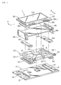
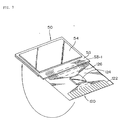
- Fig. 1 is an exploded perspective view showing an LCD device in accordance with the present invention.
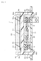
- Fig. 2 is a fragmentary sectional view taken along the line A-A of the LCD device shown in Fig. 1.
- An LCD device 1 includes, in a metal frame (not shown), a circuit board 10 serving as a second circuit board, a flexible wiring board 20 serving as a first circuit board, two conductive members 30 and 30, a structural member 40 having a light source 46 formed of an LED or the like and a light guide 44 acting as a backlight, an LCD panel 50, and spacing members 60 and 60.
- the two conductive members 30 and 30 and the flexible wiring board 20 are used for electrical connection between the LCD panel 50 and the circuit board 10.
- the flexible wiring board 20 is formed by connecting beforehand a conductive terminal 22-2, which is connected to the LCD panel 50, to a conductive terminal 53-1 of the LCD panel 50 so as to constitute a so-called COF type LCD device.
- the conductive terminal 53-1 of the LCD panel 50 is formed, for example, on an edge portion 53 of one transparent substrate 52a which constitutes the LCD panel 50 and extends beyond the other transparent substrate 52b.
- the conductive terminal 53-1 of the LCD panel 50 and the conductive terminal 22-2 of the flexible wiring board 20 are connected by thermal compression bonding via a bond capable of forming an anisotropic conductive film (ACF) that has metallic balls such as nickel balls or solder balls dispersed in a thermoplastic adhesive agent, or plastic provided with metal plating and dispersed elastic particles.
- ACF anisotropic conductive film
- the flexible wiring board 20 is bent as indicated by an arrow shown in Fig. 3 when it is used. This is because the circuit board 10 on which diverse circuits making up electronic apparatus, which will be discussed hereinafter, are mounted is disposed at the rear side of the LCD panel 50 as shown in Fig. 1. Accordingly, the exploded perspective view of Fig. 1 shows a state wherein the circuit board 10 has been disposed at the rear side of the LCD panel 50 after bending the flexible wiring board 20.
- the flexible wiring board 20 is bent, and the conductive terminals 22-1 and 22-1 provided on opposing two sides of the flexible wiring board 20 are connected to conductive terminals 12 and 12, respectively, provided on opposing two sides of the flat circuit board 10 via conductive members 30 and 30.
- Fig. 2 shows the conductive terminal 22-1 of the flexible wiring board 20 that has been connected to the conductive terminal 12 of the circuit board 10.
- the circuit board 10 disposed at the back of the LCD panel 50 is formed of, for example, a printed circuit board (PCB).
- PCB printed circuit board
- a variety of circuits including a display information processing circuit, and the like related to the LCD panel 50, a power circuit and circuits for apparatus main unit are mounted on the circuit board 10.
- the conductive terminals 12 and 12 of the diverse circuits are therefore formed on the circuit board 10.
- the flexible wiring board 20 has a predetermined pattern of wiring on the flexible board, an IC chip being mounted thereon by various methods.
- a tape carrier package (TCP) type for example, which employs a tape formed of resin such as a polyimide and a wiring layer of a metal such as copper (Cu) integrally formed with the polyimide tape or the like, and an IC chip 24 mounted on the tape, by the gang bonding process (metal eutectic bonding process) or the like.
- TCP tape carrier package
- another type may be used that has an IC chip mounted on a flexible board, which is equipped with a wiring layer, via an anisotropic conductive film (ACF), although it is not shown.
- ACF anisotropic conductive film
- the IC chip mounted on the flexible wiring board is preferably a driving circuit or the like for driving, for example, the LCD panel 50.
- a chip-type electronic part may be mounted via an ACF or by soldering.
- a conductive terminal 22-2 on the side of the LCD panel 50, and the conductive terminals 22-1 and 22-1 to be brought into contact with the conductive members 30, and the like constitute a part of the wiring pattern.
- the conductive terminal 22-2 on the side the LCD panel 50 is connected to a terminal 53-1 provided along an edge 53 of the transparent substrate 52a constituting the LCD panel 50, and the conductive terminals 22-1 of the circuit board 10 are electrically connected via the conductive members 30 to the conductive terminals 12 provided on the circuit board 10.
- This allows diverse electric signals and power to be supplied to the LCD panel 50 from the conductive terminals 12 and 12 of the circuit board 10 of the apparatus main unit via the conductive members 30, 30, the conductive terminals 22-1, 22-1, the IC chip 24, and the conductive terminal 22-2.
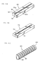
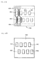
- the conductive members 30 are elastic conductors composed of, for example, elastic members; they are placed between the flexible wiring board 20 and the circuit board 10 of the apparatus main unit to elastically provide electrical connection between the conductive terminals 22-1 and the conductive terminals 12. Furthermore, the conductive members 30 function as rubber connectors (RCs), each of which having a pair of side portions 32a and 32b extending lengthwise, insulating portions 36 formed between the side portions 32a and 32b, and a plurality of conductive portions 34 which are located between the side portions 32a and 32b, formed between each of the insulating portions 36 and 36 at the same time, and arranged in a direction in which the conductive terminals 22-1 are arranged as illustrated in Fig. 4A.
- the intervals between the respective conductive portions 34 range from 30 ⁇ m to 50 ⁇ m.
- the conductive members 30 may be formed of, for example, anisotropic conductive rubber members or the like, rubber members with conductive particles dispersed therein, rubber members with thin metal lines embedded therein, or members with conductors formed in a zebra-stripe pattern.
- the conductive member may be a conductive member 70 composed of an elastic insulator 74 with a plurality of metal wires 72 made of gold or the like embedded therein as shown in Fig. 4B.
- a conductive member 80 in which a plurality of metal wires 82 made of gold or the like are provided on the outer peripheral surface of a fixing plate 84 formed to have a nearly semicircular section as illustrated in Fig. 4C. From the viewpoint of strength, the section is preferably formed to be nearly semicircular.
- the structural member 40 functions as the light guide 44 that guides an incident light from the light source 46 such as an LED toward the rear of the LCD panel 50, and it also functions as a support section for supporting the LCD panel 50. Furthermore, the structural member 40 has fixing sections 48 that project downward. The fixing sections 48 of the structural member 40 are fitted through openings 14 in the circuit board 10 of the apparatus main unit to combine the structural member 40 and the circuit board 10 into one piece. Spacing members 60, the flexible wiring board 20, and the conductive members 30 are disposed in this order from the LCD panel 50 side, being held between the structural member 40 and the circuit board 10, which are made integral by means of the fixing sections 48.
- the structural member 40 on which the LCD panel 50 is mounted can also be used as the light guide 44, so that there is no need for adding members exclusively used for fixing the members, other than the structural member 40 having the light guide 44. This permits the number of parts to be reduced and cost to be reduced accordingly especially when mass-producing LCD devices.
- the spacing members 60 installed between the structural member 40 and the flexible wiring board 20 are formed of elastic members, e.g., a rubber member made of silicone rubber, sponge members, tube members, or the like, or elastic members with air therein, plastic members, or the like.
- the spacing members 60 have plural rows of protuberances on the surfaces that are in contact with the flexible wiring board 20.
- the spacing members 60 are formed so that they have a thickness greater than a gap between the structural member 40 and the flexible wiring board 20.
- the compression rate of the spacing members 60 ranges from 15 % to 20%.
- the conductive members 30 are also formed of elastic members.
- the conductive members 30 elastically deform according to the pressure applied to the flexible wiring board 20 and the circuit board 10, and a resultant elastic force increases the contact pressure of a contact portion.
- the pressing force is generated by the structural member 40 and the spacing members 60.
- the contact reliability is improved by bringing the conductive members 30 and the respective conductive terminals 12 and 22-1 into closer contact.
- plural, e.g. two, spacing members 60 are provided so that they are associated with the positions where the conductive members 30 are disposed. This makes it possible to directly apply pressure to the points of the conductive members 30 that come in contact with the respective conductive terminals 12 and 22-1, thereby further improving the contact reliability.
- Each of the spacing members 60 in this embodiment is formed to have width W1 so that W2 ⁇ W1, where W2 denotes the width of the conductive member 30 as shown in Fig. 2. This allows the contact pressure of the flexible wiring board 20 against the conductive members 30 to be maximized, permitting further improved contact reliability.
- the members for the spacers are not limited to the examples mentioned above; they may be available in a variety of modifications, including a spacing member 90 having a nearly square section in cross section as shown in Fig. 5A, a spacing member 92 having a curved surface portion 92a which is a curved surface thereof to be in contact with a flexible wiring board as shown in Fig. 5B, a spacing member 94 having a nearly elliptic section in cross section as shown in Fig. 5C, a spacing member 96 having a protuberance 96a and a recess 96b on a surface thereof to be in contact with the flexible wiring board as shown in Fig. 5D, and a tube-like spacing member 98 having a hollow section 98a into which air is injected to secure an elastic force as shown in Fig. 5E.
- a plurality of discrete spacing members 60 are formed in relation to the conductive terminals 22-1 as shown in Fig. 1; however, the spacing members may be formed in advance according to a circuit pattern. This type of spacing members is desirable from a viewpoint of connection reliability of the conductive members 30, since they are formed beforehand according to the circuit pattern. Alternatively, the spacing member may be formed as an integral member that covers the entire rear surface of the flexible wiring board 20.
- the LCD panel 50 has two transparent substrates (poly-silicon glass substrates) 52a and 52b, liquid crystal being sealed therebetween. This constitutes at least a dot-matrix type LCD panel.
- the LCD panel 50 has polarizers 54 and 55 on the top and bottom surfaces, respectively, thereof. Circuits that are not mounted on the LCD panel 50 or the flexible wiring board 20 are handled as external circuits of the LCD panel 50; they can be mounted on the circuit board 10.
- a driving circuit, or a display information processing circuit in addition to the driving circuit, and the like may be formed on one of the transparent substrates constituting the LCD panel.
- the rear surface of the LCD panel 50 and the light guide 44 of the structural member 40 are fixed using a double-sided adhesive tape 56 or the like.
- the conductive terminal 22-2 which is located closer to the LCD panel, of the flexible wiring board 20 is electrically connected to the conductive terminal 53-1 formed on the edge portion 53 of the transparent substrate 52a of the LCD panel 50, then the LCD panel 50 and the flexible wiring board 20 are connected.
- the rear surface of the LCD panel 50 and the light guide 44 of the structural member 40 are fixed using the double-sided adhesive tapes 56 and 56.
- the flexible wiring board 20 is bent toward the rear surface of the LCD panel 50 as indicated by the arrow in Fig. 3.
- Fig. 1 and Fig. 2 since the structural member 40 is disposed at the rear of the LCD panel 50, bending the flexible wiring board 20 causes the flexible wiring board 20 to be positioned under the structural member 40 and also causes the flexible wiring board 20 to face the circuit board 10.
- the spacing members 60 are disposed between the bent flexible wiring board 20 and the structural member 40 such that they are associated to the positions where the conductive members 30 are disposed.
- the conductive members 30 and 30 are disposed between the conductive terminals 22-1 of the bent flexible wiring board 20 and the conductive terminals 12 of the circuit board 10.
- the fixing section 48 of the structural member 40 is engaged with the circuit board 10 to fix it.
- the fixing sections 48 of the structural member 40 are inserted via the openings 14 formed in the circuit board 10, and hooking sections 48a formed at the distal ends of the fixing sections 48 are engaged with the rear surface of the circuit board 10 to secure the structural member 40 and the circuit board 10 together.
- the pressure circuits for apparatus main unit are mounted on the circuit board 10.
- the conductive terminals 12 and 12 of the diverse circuits are therefore formed on the circuit board 10.
- the flexible wiring board 20 has a predetermined pattern of wiring on the flexible board, an IC chip being mounted thereon by various methods.
- a tape carrier package (TCP) type for example, which employs a tape formed of resin such as a polyimide and a wiring layer of a metal such as copper (Cu) integrally formed with the polyimide tape or the like, and an IC chip 24 mounted on the tape, by the gang bonding process (metal eutectic bonding process) or the like.
- TCP tape carrier package
- another type may be used that has an IC chip mounted on a flexible board, which is equipped with a wiring layer, via an anisotropic conductive film (ACF), although it is not shown.
- ACF anisotropic conductive film
- the IC chip mounted on the flexible wiring board is preferably a driving circuit or the like for driving, for example, the LCD panel 50.
- a chip-type electronic part may be mounted via an ACF or by soldering.
- a conductive terminal 22-2 on the side of the LCD panel 50, and the conductive terminals 22-1 and 22-1 to be brought into contact with the conductive members 30, and the like constitute a part of the wiring pattern. feature highly reliable electrical connections.
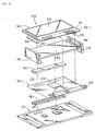
- FIG. 6 shows an example wherein the circuit pattern of the flexible wiring board is different from that in the first embodiment.
- An LCD device 100 of Fig. 6 illustrates an example of a circuit pattern on a flexible wiring board 120 wherein a conductive terminal 122 positioned on the side of a circuit board 110 and a conductive terminal 126 positioned on the side of a LCD panel 50 are formed along the long sides of the flexible wiring board 120.
- Reference numeral 124 in Fig. 6 denotes an IC chip.
- the flexible wiring board 120 is bent as shown in Fig. 7 also in the second embodiment.
- An LCD device 300 of a third embodiment in accordance with the present invention will be described with reference to Fig. 11 and Fig. 12. Members having like functions as those of the LCD device 1 of the first embodiment will be assigned like reference numerals, and the description thereof will not be repeated.
- the LCD device 300 of this embodiment mainly differs from the LCD device 1 of the first embodiment in the configuration of the structural member 40.
- the wiring pattern of a flexible wiring board 20 is identical to that of the LCD device 100 of the second embodiment.
- a conductive member 30 and a spacing member 60 disposed in association with a conductive terminal 22-1 of the flexible wiring board 20 are laid out in the same manner as the LCD device 100 of the second embodiment.
- the conductive terminals of the flexible wiring board 20 and a circuit board 10 are not shown.
- a structural member 40 of the LCD device 300 has a light guide 44, a frame section 42, and a fixing section 48.
- the light guide 44 functions to guide an incident light from a light source 46, such as an LED, toward the rear of an LCD panel 50 as in the case of the LCD device 1 of the first embodiment. Furthermore, the light guide 44 acts also as a support section on which the LCD panel 50 is rested.
- a light source 46 such as an LED
- the frame section 42 is formed of three continuous plate members provided along three sides of the edge of the light guide 44.
- a plurality of hooking members 43 that project substantially horizontally toward the inner side of the frame section 42 are provided on the top edge of the frame section 42.
- the LCD panel 50 is inserted through an opening of the frame section 42 and installed on the top surface of the light guide 44. At this time, the hooking members 43 of the frame section 42 are engaged with the top surface of the LCD panel 50 to secure the LCD panel 50 as shown in Fig. 12. In this case, it is unnecessary to fix the LCD panel 50 to the structural member 40 by a double-sided adhesive tape 56 as in the case of the LCD device 1 of the first embodiment, so that the assembly process will be simplified.
- Fixing sections 48 are formed of pin-shaped protuberances, and they project, for example, downward from the bottom surface of the light guide 44. To successfully implement the fixing and positioning function of the fixing sections 48, a plurality of, for example, four, fixing sections are provided at the four corners of the light guide 44.
- the spacing member 60, the flexible wiring board 20, and the circuit board 10 are provided with holes 62, 26, 14, respectively, in which the pin-shaped fixing sections 48 are inserted. More specifically, as shown in Fig. 11, the spacing member 60 is disposed in an area wherein the conductive terminal 22-1 is formed, the area being formed along one side of the flexible wiring board 20; hence, the spacing member 60 has two holes 62 and 62 in which the two fixing sections 48 and 48 provided on this side are inserted. Furthermore, the flexible wiring board 20 has four holes 26 and the circuit board 10 also has four holes 14, the four fixing sections 48 being inserted in the four holes of each of the two boards.
- the structural member 40, the spacing member 60, the flexible wiring board 20, and the circuit board 10 are fixed in place as shown in Fig. 12.
- the fixing sections 48 and the circuit board 10 are fixed by, for example, press-fitting the distal ends of the fixing sections 48 into the holes 14 so that a predetermined pressure can be applied to the conductive member 30 and the spacing member 60, which are formed of elastic members, by the structural member 40 and the circuit board 10.
- engaging sections may be provided at distal ends as in the case of the LCD device 1 of the first embodiment.
- the pressure produced by the elastic deformation of the spacing member 60 and the conductive member 30 brings the flexible wiring board 20 and the circuit board 10 into close contact with each other.
- the conductive member 30 is connected to the conductive terminal 12 of the circuit board 10 and the conductive terminal 22-1 of the flexible wiring board 20 to secure continuity therebetween, thus permitting easy, reliable electrical connection between the flexible wiring board 20 and the circuit board 10.
- the hooking members 43 for fixing the LCD panel 50 to the frame section 42 of the structural member 40 enables the LCD panel 50 to be fixed simply by sliding it in.
- the frame section 42 positions the LCD panel 50.
- the conductive member and the spacing member are disposed to hold the flexible wiring board therebetween, the members are pressed against each other as the structural member is fixed to the circuit board. As a result, firm and soft contact between the circuit board and the flexible wiring board can be maintained.
- Fig. 13A is an exploded perspective view showing a modification example of the structural member 40.
- the hooking members 43 for fixing the LCD panel 50 are provide integrally with the frame section 42; they are formed such that they can be deformed outward and inward with respect to the frame section 42 by elastic deformation.
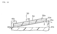
- Each of the hooking members 43 has a proximal section 43a that continues to a frame section 42 at its bottom end, and an engaging section 43b that is provided on the top end of the proximal section 43a and curved inward with respect to the frame section 42 as shown in an enlarged view of Fig. 13B.
- the LCD panel 50 is moved downward so as to cause the hooking members 43 of the structural member 40 to elastically deform outward, thereby placing the LCD panel 50 in the frame section 42. Then, the hooking members 43 restore their original states by elastic deformation, causing the LCD panel 50 to be fixed by the engaging sections 43b. In this example, it is preferable to form the hooking members 43 into a shape that permits the LCD panel 50 to be snapped in easily with a single motion.
- the top end of one plate member 42a of opposing plate members of the frame section 42 is provided with a first engaging section 43c that projects inward with respect to the frame section 42.
- the other plate member 42b is provided with a second engaging section 43d that can be elastically deformed as in the case of the hooking members 43 described above.
- a conductive terminal 184-2 on the side of an LCD panel is connected to a conductive terminal of the LCD panel, and a conductive terminal 184-1 on the side of a circuit board is connected to a conductive terminal of the circuit board as in the case of the flexible wiring board shown in Fig. 7.
- a flexible wiring board 180 is provided with a plurality of slots 182 that are located between a connection closer to the LCD panel and a connection closer to the circuit board, and disposed widthwise.
- the number of the slots 182 formed per line may be any number as necessary.
- the slots 182 may be formed in any number of lines.
- a spacing member 190 is integrally formed to cover the entire area, excluding portions 192 wherein IC chips (not shown) are formed, as illustrated in Fig. 8B, rather than forming spacing members individually at positions associated with the conductive terminal 184-1.
- the spacing member 190 may be made thinner only in the portions 192 instead of excluding them as mentioned above. With this arrangement, the number of the spacing members can be reduced.
- the individual slots are rectangular; however, the slots may take any shapes, including elliptical shapes and triangular shapes, and the spacing member may be shaped accordingly.
- Fig. 9A is an exploded perspective view showing a portable telephone 200 having an upper structural member 202 and a lower structural member 204 to which an LCD device 1 in accordance with the present invention shown in Fig. 9B has been incorporated.
- a flexible wiring board 20 of the LCD device 1 is built into the portable telephone 200 in a bent state.
- the portable telephone 200 includes more than just the LCD device 1; it includes a display information output source, a display information processing circuit, a clock generating circuit, and other diverse circuits formed on a circuit board or the like in addition to a power circuit for supplying power to these circuits.
- Electronic apparatus 300 constituted by employing the LCD device in accordance with the present invention includes a display information output source 310, a display information processing circuit 320, a display driving circuit 332, a display panel 330 such as a LCD panel 334, a clock generating circuit 340, and a power circuit 350 as shown in Fig. 10.
- the display information output source 310 is formed of memories such as a ROM and a RAM, and a tuning circuit that is tuned to television signals and outputs the signals. Based on clocks from the clock generating circuit 340, the display information output source 310 outputs video signals and other types of display information.
- the display information processing circuit 320 processes and outputs display information in response to the clocks from the clock generating circuit 340.
- the display information processing circuit 320 may include, for example, an amplifier, a polarity inverting circuit, a phase expansion circuit, a rotation circuit, a gamma control circuit, a clamp circuit, and the like.
- the display driving circuit 332 is constituted by a scanning driving circuit and a data driving circuit to drive the LCD panel 334 to perform display.
- the power circuit 350 supplies power to the respective circuits mentioned above.
- Electronic apparatus in which the LCD device in accordance with the present invention is installed is not limited to the portable telephone 200; it may be a liquid crystal projector, a multimedia-compatible personal computer (PC) or engineering workstation (EWS), a pager, a word processor, a television, a viewfinder type or a monitor direct-view type video tape recorder, an electronic pocketbook, an electronic calculator, a car navigation system, a POS terminal, a device equipped with a touch panel, a timepiece, an IC card, or a mini-disc player.
- PC personal computer
- EWS engineering workstation
- the LCD panel may be of a passive matrix LCD panel or a static drive LCD panel that does not employ switching elements for the panel itself, or an active matrix LCD panel employing a three-terminal switching element represented by a TFT or a two-terminal switching element represented by an MIM.
- various types of LCD panels may be used, including a TN type, an STN type, a guest-host type, a phase-transition type, and a ferroelectricity type.
- the embodiments have shown the examples wherein the flexible wiring boards are used to connect the LCD panels and the circuit boards.
- the present invention can also be used for connecting other types of display panels such as plasma display panels, and circuit boards.
- the present invention can also be applied for interconnecting various other types of circuit boards, in addition to the connection with the flexible wiring boards.
Landscapes
- Engineering & Computer Science (AREA)
- Physics & Mathematics (AREA)
- Microelectronics & Electronic Packaging (AREA)
- Manufacturing & Machinery (AREA)
- Nonlinear Science (AREA)
- Metallurgy (AREA)
- General Physics & Mathematics (AREA)
- Mathematical Physics (AREA)
- Chemical & Material Sciences (AREA)
- Crystallography & Structural Chemistry (AREA)
- Optics & Photonics (AREA)
- Theoretical Computer Science (AREA)
- Liquid Crystal (AREA)
- Devices For Indicating Variable Information By Combining Individual Elements (AREA)
- Combinations Of Printed Boards (AREA)
- Coupling Device And Connection With Printed Circuit (AREA)
- Multi-Conductor Connections (AREA)
Applications Claiming Priority (4)
| Application Number | Priority Date | Filing Date | Title |
|---|---|---|---|
| JP23212998 | 1998-08-18 | ||
| JP23212998 | 1998-08-18 | ||
| JP18558299A JP4298068B2 (ja) | 1998-08-18 | 1999-06-30 | 電気光学装置およびそれらを備えた電子機器並びに電気光学装置の製造方法 |
| JP18558299 | 1999-06-30 |
Publications (3)
| Publication Number | Publication Date |
|---|---|
| EP0981183A2 true EP0981183A2 (de) | 2000-02-23 |
| EP0981183A3 EP0981183A3 (de) | 2000-07-05 |
| EP0981183B1 EP0981183B1 (de) | 2007-07-11 |
Family
ID=26503196
Family Applications (1)
| Application Number | Title | Priority Date | Filing Date |
|---|---|---|---|
| EP99306481A Expired - Lifetime EP0981183B1 (de) | 1998-08-18 | 1999-08-17 | Verbindungsstruktur für Leiterplatte, elektro-optische Vorrichtung, damit versehenes elektronisches Gerät und Herstellungsverfahren für elektro-optische Vorrichtung |
Country Status (7)
| Country | Link |
|---|---|
| US (2) | US6191838B1 (de) |
| EP (1) | EP0981183B1 (de) |
| JP (1) | JP4298068B2 (de) |
| KR (1) | KR100505958B1 (de) |
| CN (1) | CN1245325A (de) |
| DE (1) | DE69936493T2 (de) |
| TW (1) | TW454162B (de) |
Cited By (9)
| Publication number | Priority date | Publication date | Assignee | Title |
|---|---|---|---|---|
| EP1001303A2 (de) * | 1998-11-11 | 2000-05-17 | Matsushita Electric Industrial Co., Ltd. | Installations- und Anschlussvorrichtung einer Anzeigeeinheit |
| EP1133014A3 (de) * | 2000-03-06 | 2002-01-23 | Hirose Electric Co., Ltd. | Elektrischer Steckverbinder |
| WO2002013327A1 (en) * | 2000-08-07 | 2002-02-14 | Teradyne, Inc. | Z-axis pressure mount connector fixture |
| EP1001304A3 (de) * | 1998-11-12 | 2004-02-11 | Matsushita Electric Industrial Co., Ltd | Flüssigkristallanzeige |
| EP1207729A3 (de) * | 2000-11-17 | 2004-03-10 | Three-Five Systems, Inc. | Gehäuse und Verfahren zum Verpacken und elektrische Verbindung eines Mikrodisplays |
| EP1403688A3 (de) * | 2002-09-24 | 2005-05-18 | Delphi Technologies, Inc. | Beleuchtung einer Flüssigkristallanzeige |
| EP1470468A4 (de) * | 2002-01-29 | 2005-07-20 | Si Han Kim | Tragbare mehrfachanzeigeeinrichtung |
| EP1344396A4 (de) * | 2000-11-22 | 2007-08-08 | Si Han Kim | Mehrfachanzeigeeinrichtung des ordnertyps |
| DE10146593B4 (de) * | 2001-09-21 | 2011-12-08 | Robert Bosch Gmbh | Anzeigevorrichtung |
Families Citing this family (83)
| Publication number | Priority date | Publication date | Assignee | Title |
|---|---|---|---|---|
| CN1166265C (zh) * | 1998-04-09 | 2004-09-08 | 精工爱普生株式会社 | 压接连接衬底、液晶装置及电子设备 |
| CN1273371C (zh) * | 1999-03-31 | 2006-09-06 | 精工爱普生株式会社 | 窄间距用连接器、间距变换装置、微机械、压电传动器、静电传动器、喷墨头、喷墨打印机、液晶面板、电子装置 |
| US6456353B1 (en) * | 1999-11-04 | 2002-09-24 | Chi Mei Opto Electronics Corp. | Display driver integrated circuit module |
| JP3622665B2 (ja) * | 1999-12-10 | 2005-02-23 | セイコーエプソン株式会社 | 接続構造、電気光学装置および電子機器 |
| JP3630116B2 (ja) | 2000-08-10 | 2005-03-16 | セイコーエプソン株式会社 | 電気光学ユニットおよび電子機器 |
| KR100396771B1 (ko) * | 2001-01-13 | 2003-09-03 | 엘지전자 주식회사 | 액정 표시 장치 및 그를 이용한 이동 단말기 |
| US6965375B1 (en) * | 2001-04-27 | 2005-11-15 | Palm, Inc. | Compact integrated touch panel display for a handheld device |
| US7692667B2 (en) * | 2001-08-17 | 2010-04-06 | Palm, Inc. | Handheld computer having moveable segments that are interactive with an integrated display |
| TWI240099B (en) * | 2001-11-06 | 2005-09-21 | Hannstar Display Corp | Method for cutting tape carrier packages of LCD and LCD structure |
| US7183582B2 (en) * | 2002-05-29 | 2007-02-27 | Seiko Epson Coporation | Electro-optical device and method of manufacturing the same, element driving device and method of manufacturing the same, element substrate, and electronic apparatus |
| US6763156B2 (en) * | 2002-06-12 | 2004-07-13 | Mcnc | Flexible optoelectronic circuit and associated method |
| US20040027526A1 (en) * | 2002-08-08 | 2004-02-12 | Hannstar Display Corporation | Liquid crystal display device |
| EP1437683B1 (de) * | 2002-12-27 | 2017-03-08 | Semiconductor Energy Laboratory Co., Ltd. | Chipkarte und Buchhaltungssystem unter Verwendung der Chipkarte |
| US7652359B2 (en) | 2002-12-27 | 2010-01-26 | Semiconductor Energy Laboratory Co., Ltd. | Article having display device |
| KR100451775B1 (ko) * | 2002-12-31 | 2004-10-08 | 엘지.필립스 엘시디 주식회사 | 터치 패널 |
| CN100507642C (zh) * | 2003-01-20 | 2009-07-01 | 瀚宇彩晶股份有限公司 | 液晶显示装置 |
| TW549474U (en) * | 2003-01-21 | 2003-08-21 | Coretronic Corp | Fixing structure for light valve |
| US7436050B2 (en) | 2003-01-22 | 2008-10-14 | Semiconductor Energy Laboratory Co., Ltd. | Semiconductor device having a flexible printed circuit |
| JP4526771B2 (ja) | 2003-03-14 | 2010-08-18 | 株式会社半導体エネルギー研究所 | 半導体装置の作製方法 |
| JP4217090B2 (ja) * | 2003-03-20 | 2009-01-28 | 株式会社 日立ディスプレイズ | 表示装置 |
| KR100908231B1 (ko) * | 2003-04-15 | 2009-07-20 | 삼성모바일디스플레이주식회사 | 평판표시소자 |
| TWI222548B (en) * | 2003-05-09 | 2004-10-21 | Benq Corp | Projector and method for assembling the projector |
| EP1498769B1 (de) * | 2003-07-15 | 2007-05-02 | Siemens Aktiengesellschaft | Metallgehäuse für eine Anzeigevorrichtung sowie Verfahren zu dessen Montage |
| US7566001B2 (en) * | 2003-08-29 | 2009-07-28 | Semiconductor Energy Laboratory Co., Ltd. | IC card |
| JP2005091971A (ja) * | 2003-09-19 | 2005-04-07 | Hitachi Displays Ltd | 表示装置 |
| JP4543772B2 (ja) * | 2003-09-19 | 2010-09-15 | セイコーエプソン株式会社 | 電気光学装置および電子機器 |
| TW594274B (en) * | 2003-10-16 | 2004-06-21 | Au Optronics Corp | Display module |
| TW594323B (en) * | 2003-10-21 | 2004-06-21 | Hannstar Display Corp | Liquid crystal system conductive line structure |
| JP3976019B2 (ja) * | 2004-02-10 | 2007-09-12 | セイコーエプソン株式会社 | 実装構造体、電気光学装置、および電子機器 |
| JP4574288B2 (ja) * | 2004-04-09 | 2010-11-04 | 大日本印刷株式会社 | リジッド−フレキシブル基板の製造方法 |
| US20050265650A1 (en) * | 2004-05-27 | 2005-12-01 | Sunil Priyadarshi | Small profile, pluggable optical transceiver subassembly |
| KR100617116B1 (ko) * | 2004-08-06 | 2006-08-31 | 엘지전자 주식회사 | 영상표시장치 |
| DE102005018336A1 (de) | 2005-02-28 | 2006-08-31 | Osram Opto Semiconductors Gmbh | Lichtleiter |
| KR100715437B1 (ko) * | 2005-06-15 | 2007-05-09 | 삼성전자주식회사 | 인쇄회로기판 |
| TWI264762B (en) * | 2005-09-05 | 2006-10-21 | Phoenix Prec Technology Corp | Optical electronics integrated semiconductor package |
| JP4579136B2 (ja) * | 2005-11-07 | 2010-11-10 | 理研計器株式会社 | 防爆型ガス検知器 |
| KR100722096B1 (ko) * | 2005-11-23 | 2007-05-25 | 삼성에스디아이 주식회사 | 휴대용 표시장치 |
| KR100715316B1 (ko) | 2006-02-13 | 2007-05-08 | 삼성전자주식회사 | 유연성 회로 기판을 이용하는 반도체 칩 패키지 실장 구조 |
| CN100501809C (zh) * | 2006-02-22 | 2009-06-17 | 朱建新 | 总线式供电显示屏 |
| US8007704B2 (en) * | 2006-07-20 | 2011-08-30 | Honeywell International Inc. | Insert molded actuator components |
| JP2008090193A (ja) * | 2006-10-04 | 2008-04-17 | Infovision Optoelectronics Holdings Ltd | 液晶表示装置用カバーユニットおよび液晶表示装置 |
| KR100800686B1 (ko) * | 2006-11-24 | 2008-02-01 | 삼성전자주식회사 | 엘시디 모듈과 그를 이용한 액정 영상 수단 |
| US7344383B1 (en) * | 2006-12-27 | 2008-03-18 | Intel Corporation | Split socket optical interconnect |
| DE102006062485A1 (de) * | 2006-12-28 | 2008-07-03 | Robert Bosch Gmbh | Elektrische Kontaktiervorrichtung, insbesondere für elektronische Schaltungen, und elektrische/elektronische Schaltung |
| JP4670855B2 (ja) * | 2007-11-08 | 2011-04-13 | セイコーエプソン株式会社 | 表示装置および時計 |
| JP2009163672A (ja) * | 2008-01-10 | 2009-07-23 | Mitsubishi Electric Corp | 表示装置 |
| US7870665B2 (en) * | 2008-03-28 | 2011-01-18 | Ibiden Co., Ltd. | Method of manufacturing a conductor circuit, and a coil sheet and laminated coil |
| TW201022765A (en) * | 2008-12-04 | 2010-06-16 | Hannspree Inc | Panel holding device and method |
| RU2444067C1 (ru) * | 2008-04-22 | 2012-02-27 | Шарп Кабусики Кайся | Электронный блок, устройство отображения и электронное устройство |
| JP4782893B2 (ja) * | 2008-04-22 | 2011-09-28 | シャープ株式会社 | 電子パッケージ、表示装置、および電子機器 |
| KR101345172B1 (ko) * | 2008-07-18 | 2013-12-27 | 엘지디스플레이 주식회사 | 전기영동 표시소자 |
| CN101770092A (zh) * | 2008-12-31 | 2010-07-07 | 群康科技(深圳)有限公司 | 液晶显示器及其框架、以及该框架的制造方法 |
| CN101842000B (zh) * | 2009-03-19 | 2014-04-30 | 鸿富锦精密工业(深圳)有限公司 | 贴附装置及使用该贴附装置的贴附方法 |
| JP5517239B2 (ja) * | 2009-11-10 | 2014-06-11 | 日本航空電子工業株式会社 | コネクタ |
| TWM381090U (en) * | 2009-11-12 | 2010-05-21 | Chunghwa Picture Tubes Ltd | Display module |
| US8644025B2 (en) * | 2009-12-22 | 2014-02-04 | Mxtran Inc. | Integrated circuit film for smart card |
| TWI473022B (zh) * | 2009-12-22 | 2015-02-11 | Mxtran Inc | 用於貼附於智慧卡之積體電路貼片 |
| JP5452290B2 (ja) * | 2010-03-05 | 2014-03-26 | ラピスセミコンダクタ株式会社 | 表示パネル |
| JP2012088605A (ja) * | 2010-10-21 | 2012-05-10 | Hitachi Displays Ltd | 表示装置 |
| US9179560B2 (en) * | 2010-10-25 | 2015-11-03 | Korea Electric Terminal Co., Ltd. | Board block for vehicles |
| KR20120049019A (ko) * | 2010-11-08 | 2012-05-16 | 삼성모바일디스플레이주식회사 | 정전용량형 터치 패널 |
| JP5754956B2 (ja) * | 2011-01-27 | 2015-07-29 | サトーホールディングス株式会社 | プリンタの情報表示器 |
| CN102645762A (zh) * | 2011-02-18 | 2012-08-22 | 鸿富锦精密工业(深圳)有限公司 | 显示装置 |
| CN102738609A (zh) * | 2011-04-06 | 2012-10-17 | 鸿富锦精密工业(深圳)有限公司 | 电子元件固定装置 |
| JP2012222577A (ja) * | 2011-04-07 | 2012-11-12 | Funai Electric Co Ltd | 機器基板取付け構造 |
| JP5518806B2 (ja) * | 2011-08-04 | 2014-06-11 | 株式会社ソニー・コンピュータエンタテインメント | 電子機器 |
| KR101878179B1 (ko) * | 2011-11-23 | 2018-07-16 | 엘지디스플레이 주식회사 | 구동회로기판 및 이를 포함하는 액정표시장치 |
| US8870440B2 (en) * | 2012-03-30 | 2014-10-28 | Shenzhen China Star Optoelectronics Technology Co., Ltd. | Back light module and liquid crystal display device having the same |
| US9368427B2 (en) | 2013-02-01 | 2016-06-14 | Mxtran Inc. | Integrated circuit film and method of manufacturing the same |
| US9418254B2 (en) * | 2013-02-01 | 2016-08-16 | Mxtran Inc. | Integrated circuit film and method for manipulating the same |
| US10852025B2 (en) | 2013-04-30 | 2020-12-01 | Ademco Inc. | HVAC controller with fixed segment display having fixed segment icons and animation |
| DE102013008433B4 (de) * | 2013-05-17 | 2020-12-03 | Lisa Dräxlmaier GmbH | Flächige Vorrichtung zur Beleuchtung der Innenausstattung eines Fahrzeugs |
| JP6511468B2 (ja) * | 2013-11-28 | 2019-05-15 | ジオ・オプトエレクトロニクス・コーポレイションGio Optoelectronics Corp. | マトリクス回路基板、ディスプレイ装置、およびマトリクス回路基板の製造方法 |
| KR102107456B1 (ko) * | 2013-12-10 | 2020-05-08 | 삼성디스플레이 주식회사 | 플렉시블 표시 장치 및 이의 제조 방법 |
| KR102232424B1 (ko) * | 2014-09-19 | 2021-03-29 | 삼성디스플레이 주식회사 | 표시모듈 조립용 압착패드 및 표시모듈 조립 방법 |
| WO2017209315A1 (ko) * | 2016-05-30 | 2017-12-07 | 주식회사 옵텔라 | 전기 인터페이스 결합구조 |
| JP6781021B2 (ja) * | 2016-11-29 | 2020-11-04 | モレックス エルエルシー | 電子部品 |
| TWI692152B (zh) * | 2017-02-07 | 2020-04-21 | 美商莫仕有限公司 | 電連接裝置及板對板電連接組合 |
| EP3595274B1 (de) * | 2017-05-24 | 2021-01-13 | Guangdong Oppo Mobile Telecommunications Corp., Ltd. | Halterung für elektronische komponente, anordnung elektronischer komponenten und mobiles endgerät |
| WO2019123647A1 (ja) * | 2017-12-22 | 2019-06-27 | 堺ディスプレイプロダクト株式会社 | 表示装置および表示装置の製造方法 |
| KR102803442B1 (ko) * | 2019-12-11 | 2025-05-07 | 삼성전기주식회사 | 인쇄회로기판, 이를 포함하는 디스플레이 장치, 및 인쇄회로기판의 제조방법 |
| CN110910780A (zh) * | 2019-12-23 | 2020-03-24 | 深圳市铭濠科技有限公司 | 一种led智能云屏驱动盒拼接的显示屏 |
| KR102822090B1 (ko) * | 2020-12-08 | 2025-06-17 | 콘티넨탈 오토모티브 테크놀로지스 게엠베하 | 2개의 상호 연결된 요소를 가진 전기광학 디스플레이 모듈 |
Family Cites Families (18)
| Publication number | Priority date | Publication date | Assignee | Title |
|---|---|---|---|---|
| FR2495846A1 (fr) * | 1980-12-05 | 1982-06-11 | Cii Honeywell Bull | Dispositif de connexion electrique a haute densite de contacts |
| FR2515401A1 (fr) * | 1981-10-23 | 1983-04-29 | Thomson Csf | Dispositif de connexion et d'alignement d'un faisceau de fils en nappe avec les pistes conductrices correspondantes portees par un substrat et systeme d'affichage comprenant un tel dispositif |
| US4598960A (en) * | 1985-04-29 | 1986-07-08 | Copytele, Inc. | Methods and apparatus for connecting closely spaced large conductor arrays employing multi-conductor carrier boards |
| US4695258A (en) * | 1986-12-09 | 1987-09-22 | Cherne Industries, Inc. | Connector assembly for electrically connecting flexible and rigid printed circuits |
| US5164853A (en) * | 1989-04-06 | 1992-11-17 | Ricoh Company, Ltd. | Liquid crystal display panel with plural substrates |
| JP2846751B2 (ja) * | 1991-07-03 | 1999-01-13 | ローム株式会社 | 回路基板に対するフレキシブルケーブルの接続装置 |
| JP3205373B2 (ja) * | 1992-03-12 | 2001-09-04 | 株式会社日立製作所 | 液晶表示装置 |
| DE4236353C2 (de) * | 1992-10-28 | 1995-03-23 | Preh Elektro Feinmechanik | Elektrische Baugruppe |
| US5358412A (en) * | 1993-04-26 | 1994-10-25 | Eastman Kodak Company | Method and apparatus for assembling a flexible circuit to an LCD module |
| JP3184853B2 (ja) * | 1993-06-24 | 2001-07-09 | 株式会社日立製作所 | 液晶表示装置 |
| JP2980496B2 (ja) * | 1993-11-10 | 1999-11-22 | シャープ株式会社 | フレキシブル配線板の端子構造 |
| US5640216A (en) * | 1994-04-13 | 1997-06-17 | Hitachi, Ltd. | Liquid crystal display device having video signal driving circuit mounted on one side and housing |
| JP2891875B2 (ja) * | 1994-06-09 | 1999-05-17 | 日本電気株式会社 | 液晶表示装置 |
| JPH08186336A (ja) * | 1994-12-28 | 1996-07-16 | Mitsubishi Electric Corp | 回路基板、駆動回路モジュール及びそれを用いた液晶表示装置並びにそれらの製造方法 |
| US5936850A (en) * | 1995-03-03 | 1999-08-10 | Canon Kabushiki Kaisha | Circuit board connection structure and method, and liquid crystal device including the connection structure |
| JP3127774B2 (ja) * | 1995-03-31 | 2001-01-29 | セイコーエプソン株式会社 | シールド材および液晶表示装置 |
| CN1097255C (zh) | 1995-06-29 | 2002-12-25 | 龙野机电技术股份公司 | 用于给油机显示装置 |
| JPH09218394A (ja) * | 1996-02-09 | 1997-08-19 | Asahi Optical Co Ltd | 液晶表示板固定具 |
-
1999
- 1999-06-30 JP JP18558299A patent/JP4298068B2/ja not_active Expired - Lifetime
- 1999-08-05 TW TW088113411A patent/TW454162B/zh not_active IP Right Cessation
- 1999-08-16 KR KR10-1999-0033604A patent/KR100505958B1/ko not_active Expired - Lifetime
- 1999-08-17 DE DE69936493T patent/DE69936493T2/de not_active Expired - Lifetime
- 1999-08-17 EP EP99306481A patent/EP0981183B1/de not_active Expired - Lifetime
- 1999-08-17 US US09/375,993 patent/US6191838B1/en not_active Expired - Lifetime
- 1999-08-17 CN CN99119510A patent/CN1245325A/zh active Pending
-
2000
- 2000-12-05 US US09/730,041 patent/US6675470B2/en not_active Expired - Lifetime
Cited By (10)
| Publication number | Priority date | Publication date | Assignee | Title |
|---|---|---|---|---|
| EP1001303A2 (de) * | 1998-11-11 | 2000-05-17 | Matsushita Electric Industrial Co., Ltd. | Installations- und Anschlussvorrichtung einer Anzeigeeinheit |
| EP1001304A3 (de) * | 1998-11-12 | 2004-02-11 | Matsushita Electric Industrial Co., Ltd | Flüssigkristallanzeige |
| EP1133014A3 (de) * | 2000-03-06 | 2002-01-23 | Hirose Electric Co., Ltd. | Elektrischer Steckverbinder |
| WO2002013327A1 (en) * | 2000-08-07 | 2002-02-14 | Teradyne, Inc. | Z-axis pressure mount connector fixture |
| EP1207729A3 (de) * | 2000-11-17 | 2004-03-10 | Three-Five Systems, Inc. | Gehäuse und Verfahren zum Verpacken und elektrische Verbindung eines Mikrodisplays |
| EP1344396A4 (de) * | 2000-11-22 | 2007-08-08 | Si Han Kim | Mehrfachanzeigeeinrichtung des ordnertyps |
| DE10146593B4 (de) * | 2001-09-21 | 2011-12-08 | Robert Bosch Gmbh | Anzeigevorrichtung |
| EP1470468A4 (de) * | 2002-01-29 | 2005-07-20 | Si Han Kim | Tragbare mehrfachanzeigeeinrichtung |
| EP1731986A3 (de) * | 2002-01-29 | 2007-01-03 | Si Han Kim | Tragbare Multianzeigevorrichtung |
| EP1403688A3 (de) * | 2002-09-24 | 2005-05-18 | Delphi Technologies, Inc. | Beleuchtung einer Flüssigkristallanzeige |
Also Published As
| Publication number | Publication date |
|---|---|
| DE69936493D1 (de) | 2007-08-23 |
| DE69936493T2 (de) | 2008-03-20 |
| JP4298068B2 (ja) | 2009-07-15 |
| US20010000763A1 (en) | 2001-05-03 |
| KR20000017323A (ko) | 2000-03-25 |
| JP2000133904A (ja) | 2000-05-12 |
| EP0981183B1 (de) | 2007-07-11 |
| EP0981183A3 (de) | 2000-07-05 |
| US6191838B1 (en) | 2001-02-20 |
| US6675470B2 (en) | 2004-01-13 |
| CN1245325A (zh) | 2000-02-23 |
| KR100505958B1 (ko) | 2005-08-04 |
| TW454162B (en) | 2001-09-11 |
Similar Documents
| Publication | Publication Date | Title |
|---|---|---|
| EP0981183B1 (de) | Verbindungsstruktur für Leiterplatte, elektro-optische Vorrichtung, damit versehenes elektronisches Gerät und Herstellungsverfahren für elektro-optische Vorrichtung | |
| KR100339646B1 (ko) | 매트릭스 표시 장치 및 그 제조 방법 그리고 열압착 접속용 헤드 | |
| US6729888B2 (en) | Connecting structure, electro-optical device, and electronic apparatus | |
| US4514042A (en) | Thin structure of display panel | |
| US6025644A (en) | Liquid crystal display and apparatus using the same | |
| JP3284262B2 (ja) | 液晶表示装置及びそれを用いた電子機器 | |
| EP0795772A1 (de) | Kontaktierungsstruktur für Treiberschaltung und Anzeigevorrichtung mit dieser Kontaktierungsstruktur | |
| US6300998B1 (en) | Probe for inspecting liquid crystal display panel, and apparatus and method for inspecting liquid crystal display panel | |
| JP2002091335A (ja) | フレキシブル基板のケースおよび液晶表示モジュール | |
| US5978060A (en) | Liquid crystal display apparatus and apparatus for manufacturing the same | |
| JP3431447B2 (ja) | 表示装置 | |
| KR100735988B1 (ko) | 전기 광학 장치 및 전자기기 | |
| JP2001230001A (ja) | 接続構造、電気光学装置および電子機器 | |
| JPH05142558A (ja) | 液晶表示装置 | |
| JP2894728B2 (ja) | 液晶表示装置およびその製造方法 | |
| JPH04225327A (ja) | 電子回路の実装構造及びそれを用いた電子光学装置及び電子印字装置 | |
| JP3757779B2 (ja) | 液晶表示装置 | |
| JP2007329316A (ja) | 配線基板及び実装構造体 | |
| JP2001125129A (ja) | 液晶表示装置 | |
| JPH0996828A (ja) | 液晶表示装置 | |
| JPH10206820A (ja) | 液晶表示装置 | |
| JP2001242800A (ja) | 電気光学装置及び電子機器 | |
| JPS6261089A (ja) | 平面表示装置 | |
| JP2000002883A (ja) | 液晶表示素子 | |
| JP2005043903A (ja) | 液晶表示装置及びその使用機器 |
Legal Events
| Date | Code | Title | Description |
|---|---|---|---|
| PUAI | Public reference made under article 153(3) epc to a published international application that has entered the european phase |
Free format text: ORIGINAL CODE: 0009012 |
|
| AK | Designated contracting states |
Kind code of ref document: A2 Designated state(s): DE FR GB |
|
| AX | Request for extension of the european patent |
Free format text: AL;LT;LV;MK;RO;SI |
|
| PUAL | Search report despatched |
Free format text: ORIGINAL CODE: 0009013 |
|
| AK | Designated contracting states |
Kind code of ref document: A3 Designated state(s): AT BE CH CY DE DK ES FI FR GB GR IE IT LI LU MC NL PT SE |
|
| AX | Request for extension of the european patent |
Free format text: AL;LT;LV;MK;RO;SI |
|
| RIC1 | Information provided on ipc code assigned before grant |
Free format text: 7H 01R 12/12 A, 7H 01R 12/14 B |
|
| 17P | Request for examination filed |
Effective date: 20001127 |
|
| AKX | Designation fees paid |
Free format text: DE FR GB |
|
| 17Q | First examination report despatched |
Effective date: 20050225 |
|
| GRAP | Despatch of communication of intention to grant a patent |
Free format text: ORIGINAL CODE: EPIDOSNIGR1 |
|
| GRAS | Grant fee paid |
Free format text: ORIGINAL CODE: EPIDOSNIGR3 |
|
| GRAA | (expected) grant |
Free format text: ORIGINAL CODE: 0009210 |
|
| AK | Designated contracting states |
Kind code of ref document: B1 Designated state(s): DE FR GB |
|
| REG | Reference to a national code |
Ref country code: GB Ref legal event code: FG4D |
|
| REF | Corresponds to: |
Ref document number: 69936493 Country of ref document: DE Date of ref document: 20070823 Kind code of ref document: P |
|
| ET | Fr: translation filed | ||
| PLBE | No opposition filed within time limit |
Free format text: ORIGINAL CODE: 0009261 |
|
| STAA | Information on the status of an ep patent application or granted ep patent |
Free format text: STATUS: NO OPPOSITION FILED WITHIN TIME LIMIT |
|
| 26N | No opposition filed |
Effective date: 20080414 |
|
| PGFP | Annual fee paid to national office [announced via postgrant information from national office to epo] |
Ref country code: DE Payment date: 20110810 Year of fee payment: 13 Ref country code: FR Payment date: 20110818 Year of fee payment: 13 Ref country code: GB Payment date: 20110817 Year of fee payment: 13 |
|
| GBPC | Gb: european patent ceased through non-payment of renewal fee |
Effective date: 20120817 |
|
| REG | Reference to a national code |
Ref country code: FR Ref legal event code: ST Effective date: 20130430 |
|
| PG25 | Lapsed in a contracting state [announced via postgrant information from national office to epo] |
Ref country code: DE Free format text: LAPSE BECAUSE OF NON-PAYMENT OF DUE FEES Effective date: 20130301 Ref country code: GB Free format text: LAPSE BECAUSE OF NON-PAYMENT OF DUE FEES Effective date: 20120817 |
|
| PG25 | Lapsed in a contracting state [announced via postgrant information from national office to epo] |
Ref country code: FR Free format text: LAPSE BECAUSE OF NON-PAYMENT OF DUE FEES Effective date: 20120831 |
|
| REG | Reference to a national code |
Ref country code: DE Ref legal event code: R119 Ref document number: 69936493 Country of ref document: DE Effective date: 20130301 |