EP0982664A2 - Verknüpfung eines Hauptprozessors an ein Speicherungsuntersystem - Google Patents
Verknüpfung eines Hauptprozessors an ein Speicherungsuntersystem Download PDFInfo
- Publication number
- EP0982664A2 EP0982664A2 EP99306240A EP99306240A EP0982664A2 EP 0982664 A2 EP0982664 A2 EP 0982664A2 EP 99306240 A EP99306240 A EP 99306240A EP 99306240 A EP99306240 A EP 99306240A EP 0982664 A2 EP0982664 A2 EP 0982664A2
- Authority
- EP
- European Patent Office
- Prior art keywords
- script
- bus system
- data
- memory subsystem
- host processor
- Prior art date
- Legal status (The legal status is an assumption and is not a legal conclusion. Google has not performed a legal analysis and makes no representation as to the accuracy of the status listed.)
- Withdrawn
Links
Images

Classifications
-
- G—PHYSICS
- G06—COMPUTING OR CALCULATING; COUNTING
- G06F—ELECTRIC DIGITAL DATA PROCESSING
- G06F13/00—Interconnection of, or transfer of information or other signals between, memories, input/output devices or central processing units
-
- G—PHYSICS
- G06—COMPUTING OR CALCULATING; COUNTING
- G06F—ELECTRIC DIGITAL DATA PROCESSING
- G06F13/00—Interconnection of, or transfer of information or other signals between, memories, input/output devices or central processing units
- G06F13/14—Handling requests for interconnection or transfer
- G06F13/16—Handling requests for interconnection or transfer for access to memory bus
Definitions
- This invention relates to a system for coupling a host processor and a memory subsystem in such a manner as to enable efficient transfers of data therebetween.
- Computer systems typically include more than one bus, each bus having attached devices which communicate locally with each other.
- system busses and peripheral busses use different sets of standard protocols or rules to conduct data transfers between the different devices that are connected thereover.
- Devices for translating data that is transferred from one bus architecture to another bus architecture are often called bridges.
- bus-to-bus bridges match the communications protocol of one bus architecture with that of another bus architecture.
- PCI peripheral component interconnect
- a second bridge circuit (also called a bus controller) provides an interface for transfer of data between a further bus system and the PCI bus.
- the arrangement is such that devices on the PCI bus transfer data to and receive data via the first bridge, while devices coupled to the second bus system transfer and receive data through the second bridge (or bus controller).
- the two bridges communicate with each other and enable data transfers between devices connected to the PCI bus and the second bus system.
- SCSI small computer system interconnect
- An example of such a message is a status indication that is issued by a memory subsystem to indicate the success or failure of a read/write action. Such a status message is dispatched to the host processor which initiated the read or write request.
- a system for coupling a host processor to a memory subsystem comprising: a first bus system operated in accord with a first protocol coupled to the memory subsystem; controller means coupled to the first bus system and the host processor and including memory for storing plural Scripts, each of the plural Scripts comprising a set of instructions for performing an operation and including an address where Script data can be found which is to accompany the respective Script; and processor means for providing to the controller means, an instruction operable to play a designated Script, the play causing Script data, designated by an address in the designated Script, to be accessed and to be transmitted with the designated Script.
- a computing system forming one embodiment of the invention includes a host processor which is coupled to a memory subsystem via a first bus system, a controller device and a second bus system.
- the controller device includes memory for storing plural Scripts for replay to the host processor, for instance, via the second bus system.
- a Script is an instruction set used to execute operations on a controller device. Each Script includes one or more addresses where either message or status data (or other operational data) can be found which is to be inserted, prior to dispatch of the Script.
- the memory subsystem is caused, as a result of its operation, to issue an instruction to the controller device to dispatch a Script to, for instance, the host processor.
- the controller device responds by accessing the required Script, playing the Script which results in accesses to locally stored operational data for inclusion into the Script. Local storage of this data avoids unnecessary data transfers over the bus system to the memory subsystem to obtain the required data for inclusion into a Script.
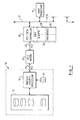
- a memory subsystem 10 includes a plurality of disk drives 12 that are coupled to a memory system processor 14. Memory subsystem 10 thus acts as a central data repository for one or more host processors 16. Host processor 16 is coupled via a SCSI bus 17 to a PCI/SCSI controller 18. In turn, PCI/SCSI controller 18 is coupled to a PCI bridge 20 via PCI bus 22. PCI bridge 20 is, in turn, coupled to memory system processor 14 via PCI bus 24.
- various status and operational messages are required to be dispatched to host processor 16 for the purpose of overall system control and administration. Such messages include various status data regarding the success or lack of success of read/write actions. Other operational information regarding the memory subsystem 10 is also required to be dispatched at certain times during the operation of the computing system.
- PCI/SCSI controller 18 is provided with a random access memory (RAM) 26 which includes capacity for the storage of plural "Scripts" 28.
- RAM 26 further includes a plurality of "mailboxes" 30 that serve as repositories of specific operational data that are referenced by one or more Scripts 28.
- Each Script 28 is a subroutine which, upon dispatch and receipt by a recipient, enables the recipient to accomplish a required action or to register a segment of data contained within a Script.
- one such Script may, upon dispatch from PCI/SCSI controller 18 to memory system processor 14, cause memory subsystem 10 to commence a read action in accordance with data contained within the Script.
- a similar Script can cause a write action to be processed by memory subsystem 10.
- Still another Script might comprise a message which indicates the status of a particular element of the computing system (e.g. operative, inoperative, off-line, etc.).
- Still other types of Scripts may be utilized to dispatch a particular operation message such as a "disconnect", "connect,” “identify” or other similar actions.
- Each Script 28 is associated with a particular message or operational indication. Accordingly, if memory system processor 14 successfully completes a read action, it dispatches a message to PCI/SCSI controller 18 to play a particular Script that indicates to host processor 16 the successful completion of the read action. To avoid PCI/SCSI controller 18 having to access operational data directly from memory system processor 14 in response to the aforesaid message, Script 28, when played, accesses a mailbox 30 which includes the relevant data to be included in the Script. Such data indicates the successful completion of the read action.
- each mailbox 30 is essentially an address in RAM 26 wherein specific data can be found that is to be included in a Script. Such data is accessed when a Script is played and an address of a respective mailbox is encountered that has been embedded in the Script during initialization time.
- the data in a mailbox may be reserved for a single Script or may be common data that is used by plural Scripts. In either case, the respective Script(s) will have embedded therein the address where such data can be found that is to be inserted in the Script. Accordingly, when any Script is played, and a line thereof is reached which includes the address of a particular mailbox, that mailbox is accessed and the data resident therein is automatically inserted into the Script and is played as though already present in the Script.
- PCS/SCSI controller 18 is loaded with all required Scripts.
- the Scripts may be loaded from memory system processor 14, which accesses the particular Scripts from one or more disk drives 12 or, directly from host processor 16 (step 50).
- operational data are loaded into "mailboxes" at preset addresses in RAM 26 (step 52). Note that there are additional predefined mailbox areas which follow the status/message mailbox locations in RAM - for other operational data.
- each Script is "patched" with the preset address(s) for the operational data that are to be inserted when the Script is played.
- memory system processor 14 During the execution phase of the procedure, assume that memory system processor 14 is to issue a status message to host processor 16. Accordingly, memory system processor 14 dispatches a message to PCI/SCSI controller 18 (via PCI bridge 20), to dispatch a designated Script to host processor 12 (step 56). PCI/SCSI controller 18 responds by accessing and playing the designated Script. During play of the Script, each line thereof which includes a mailbox address causes the addressed data in the designated mailbox 30 to be accessed. The data contained within the respective mailbox 30 is then inserted into code stream comprising the Script and is sent, for example, to host processor 16 (step 58).
- a Script may include one, some or many mailbox addresses, depending upon the number of pre-defined operational data values that are to be inserted therein for execution during runtime.
- the invention avoids the need for many PCI bus interface/access actions, as most, if not all of the necessary operational data is downloaded to PCI/SCSI controller 18 during the initialization phase or is accessed at runtime via mailbox addresses in local memory. Therefore, when any Script is to be played, all that is required is for memory system processor 14, for instance, to designate a particular Script by dispatching a one or two-byte value to PCI/SCSI controller 18.
Landscapes
- Engineering & Computer Science (AREA)
- Theoretical Computer Science (AREA)
- Physics & Mathematics (AREA)
- General Engineering & Computer Science (AREA)
- General Physics & Mathematics (AREA)
- Bus Control (AREA)
- Advance Control (AREA)
Applications Claiming Priority (2)
| Application Number | Priority Date | Filing Date | Title |
|---|---|---|---|
| US09/138,118 US6065083A (en) | 1998-08-21 | 1998-08-21 | Increasing I/O performance through storage of packetized operational information in local memory |
| US138118 | 1998-08-21 |
Publications (2)
| Publication Number | Publication Date |
|---|---|
| EP0982664A2 true EP0982664A2 (de) | 2000-03-01 |
| EP0982664A3 EP0982664A3 (de) | 2004-01-14 |
Family
ID=22480497
Family Applications (1)
| Application Number | Title | Priority Date | Filing Date |
|---|---|---|---|
| EP99306240A Withdrawn EP0982664A3 (de) | 1998-08-21 | 1999-08-06 | Verknüpfung eines Hauptprozessors an ein Speicherungsuntersystem |
Country Status (6)
| Country | Link |
|---|---|
| US (1) | US6065083A (de) |
| EP (1) | EP0982664A3 (de) |
| JP (1) | JP3475130B2 (de) |
| KR (1) | KR100316190B1 (de) |
| SG (1) | SG77706A1 (de) |
| TW (1) | TW434491B (de) |
Families Citing this family (12)
| Publication number | Priority date | Publication date | Assignee | Title |
|---|---|---|---|---|
| US6615279B1 (en) * | 1997-01-29 | 2003-09-02 | Iq Systems | Central and distributed script servers in an object oriented processor array |
| US6185607B1 (en) * | 1998-05-26 | 2001-02-06 | 3Com Corporation | Method for managing network data transfers with minimal host processor involvement |
| KR20020032136A (ko) * | 2000-10-25 | 2002-05-03 | 박성훈 | 메모리를 이용한 대용량 보조기억장치 |
| US7315551B2 (en) * | 2002-03-15 | 2008-01-01 | Lockheed Martin Corporation | Synchronous low voltage differential I/O buss |
| KR100467102B1 (ko) * | 2002-05-28 | 2005-01-24 | (주) 그레이프테크놀로지 | 데이터 저장 시스템 |
| US6941408B2 (en) * | 2002-09-30 | 2005-09-06 | Lsi Logic Corporation | Bus interface system with two separate data transfer interfaces |
| WO2006071817A2 (en) * | 2004-12-29 | 2006-07-06 | Netcell Corporation | Intelligent storage engine for disk drive operations with reduced local bus traffic |
| US20070076912A1 (en) * | 2005-09-30 | 2007-04-05 | Griffiths Richard D | Audio speaker enclosures |
| US20150109457A1 (en) * | 2012-10-04 | 2015-04-23 | Jigabot, Llc | Multiple means of framing a subject |
| KR101619625B1 (ko) | 2014-10-22 | 2016-05-10 | 현대자동차주식회사 | 자동차용 인사이드 미러 조립체 |
| KR20240164976A (ko) | 2023-05-15 | 2024-11-22 | 최소영 | 발음을 이야기 카드 방식으로 가르치기 위한 아동용 발음 학습교구 및 그 교구를 활용한 교수법 |
| KR20240164977A (ko) | 2023-05-15 | 2024-11-22 | 최소영 | 화용언어 학습용 만화교재 및 그 교재를 활용한 교수법 |
Citations (1)
| Publication number | Priority date | Publication date | Assignee | Title |
|---|---|---|---|---|
| US5634033A (en) * | 1994-12-16 | 1997-05-27 | At&T Global Information Solutions Company | Disk array storage system architecture for parity operations simultaneous with other data operations |
Family Cites Families (12)
| Publication number | Priority date | Publication date | Assignee | Title |
|---|---|---|---|---|
| US4916539A (en) * | 1983-04-21 | 1990-04-10 | The Weather Channel, Inc. | Communications system having receivers which can be addressed in selected classes |
| EP0837391B1 (de) * | 1990-08-31 | 2002-05-29 | Texas Instruments Incorporated | Multiprozessorsystem |
| US5341474A (en) * | 1992-05-15 | 1994-08-23 | Bell Communications Research, Inc. | Communications architecture and buffer for distributing information services |
| JPH06110824A (ja) * | 1992-09-25 | 1994-04-22 | Fuji Xerox Co Ltd | バスブリッジ装置 |
| US5623656A (en) * | 1994-12-15 | 1997-04-22 | Lucent Technologies Inc. | Script-based data communication system and method utilizing state memory |
| KR960025034A (ko) * | 1994-12-28 | 1996-07-20 | 김용현 | 알아이에스씨(risc) 씨피유(cpu)를 채용한 멀티포트 로컬 브리지 |
| JPH08314850A (ja) * | 1995-05-17 | 1996-11-29 | Toshiba Corp | 計算機システムのバスブリッジ |
| KR100234687B1 (ko) * | 1996-04-04 | 1999-12-15 | 김영환 | 브리지 회로 |
| US5822549A (en) * | 1996-07-15 | 1998-10-13 | Micron Electronics, Inc. | Computer system and bus controller for controlling access to a computer bus |
| US5933610A (en) * | 1996-09-17 | 1999-08-03 | Vlsi Technology, Inc. | Predictive arbitration system for PCI bus agents |
| US5915124A (en) * | 1997-01-03 | 1999-06-22 | Ncr Corporation | Method and apparatus for a first device accessing computer memory and a second device detecting the access and responding by performing sequence of actions |
| US5909559A (en) * | 1997-04-04 | 1999-06-01 | Texas Instruments Incorporated | Bus bridge device including data bus of first width for a first processor, memory controller, arbiter circuit and second processor having a different second data width |
-
1998
- 1998-08-21 US US09/138,118 patent/US6065083A/en not_active Expired - Fee Related
-
1999
- 1999-07-15 KR KR1019990028649A patent/KR100316190B1/ko not_active Expired - Fee Related
- 1999-08-06 SG SG1999003845A patent/SG77706A1/en unknown
- 1999-08-06 EP EP99306240A patent/EP0982664A3/de not_active Withdrawn
- 1999-08-11 JP JP22704099A patent/JP3475130B2/ja not_active Expired - Fee Related
- 1999-09-03 TW TW088114102A patent/TW434491B/zh not_active IP Right Cessation
Patent Citations (1)
| Publication number | Priority date | Publication date | Assignee | Title |
|---|---|---|---|---|
| US5634033A (en) * | 1994-12-16 | 1997-05-27 | At&T Global Information Solutions Company | Disk array storage system architecture for parity operations simultaneous with other data operations |
Also Published As
| Publication number | Publication date |
|---|---|
| JP2000112866A (ja) | 2000-04-21 |
| SG77706A1 (en) | 2001-01-16 |
| KR100316190B1 (ko) | 2001-12-12 |
| TW434491B (en) | 2001-05-16 |
| JP3475130B2 (ja) | 2003-12-08 |
| US6065083A (en) | 2000-05-16 |
| KR20000016944A (ko) | 2000-03-25 |
| EP0982664A3 (de) | 2004-01-14 |
Similar Documents
| Publication | Publication Date | Title |
|---|---|---|
| US6321279B1 (en) | System for implementing intelligent I/O processing in a multi-processor system by redirecting I/O messages to a target central processor selected from the multi-processor system | |
| US7225326B2 (en) | Hardware assisted ATA command queuing | |
| US5940866A (en) | Information handling system having a local address queue for local storage of command blocks transferred from a host processing side | |
| US6564271B2 (en) | Method and apparatus for automatically transferring I/O blocks between a host system and a host adapter | |
| US5590376A (en) | Apparatus and method for detecting and updating status of removable storage system using shared interrupt and software flag | |
| US6298399B1 (en) | System for managing input/output accesses at a bridge/memory controller having a status register for recording cause of interrupt | |
| US6065083A (en) | Increasing I/O performance through storage of packetized operational information in local memory | |
| EP0712084A1 (de) | Direktspeicherzugriff-Emulation | |
| JPH09160861A (ja) | ローカル・プロセッサの介入なしにコマンド・ブロックをローカル処理サイドに転送するための情報処理システム | |
| CN87106353A (zh) | 数字数据处理系统高速缓冲存储器内容的失效标记 | |
| JPH04318649A (ja) | データ処理システム | |
| EP0524936A1 (de) | Datenübertragung innerhalb eines datenspeicheruntersystems | |
| US6105080A (en) | Host adapter DMA controller with automated host reply capability | |
| US4729091A (en) | Directing storage requests prior to address comparator initialization with a reference address range | |
| KR20010040936A (ko) | 2차 버스로부터의 메시징 유닛 액세스 | |
| US5832246A (en) | Virtualization of the ISA bus on PCI with the existence of a PCI to ISA bridge | |
| JP4359618B2 (ja) | コンフィグレーション・レジスター・アクセス方法、設定方法、集積回路部品、コンピューター・システム、製品 | |
| JP4664077B2 (ja) | 光学ストレージの転送性能の向上 | |
| US6466996B1 (en) | Method and system for implementing intelligent distributed input-output processing as a software process in a host operating system environment | |
| US6108723A (en) | System for implementing hardware automated control of burst mode data transfer over a communication link between devices operating in a block mode | |
| US6134623A (en) | Method and system for taking advantage of a pre-stage of data between a host processor and a memory system | |
| JP3110024B2 (ja) | メモリ制御システム | |
| JPH0962633A (ja) | ネットワーク制御装置 | |
| JP2008503833A (ja) | 並列通信バスに連結された装置内で割込みメッセージを待ち行列に入れるためのコンピュータシステム及び方法 | |
| JPH0816405A (ja) | システム初期化装置 |
Legal Events
| Date | Code | Title | Description |
|---|---|---|---|
| PUAI | Public reference made under article 153(3) epc to a published international application that has entered the european phase |
Free format text: ORIGINAL CODE: 0009012 |
|
| AK | Designated contracting states |
Kind code of ref document: A2 Designated state(s): AT BE CH CY DE DK ES FI FR GB GR IE IT LI LU MC NL PT SE |
|
| AX | Request for extension of the european patent |
Free format text: AL;LT;LV;MK;RO;SI |
|
| PUAL | Search report despatched |
Free format text: ORIGINAL CODE: 0009013 |
|
| AK | Designated contracting states |
Kind code of ref document: A3 Designated state(s): AT BE CH CY DE DK ES FI FR GB GR IE IT LI LU MC NL PT SE |
|
| AX | Request for extension of the european patent |
Extension state: AL LT LV MK RO SI |
|
| 17P | Request for examination filed |
Effective date: 20040128 |
|
| AKX | Designation fees paid |
Designated state(s): AT BE CH CY DE DK ES FI FR GB GR IE IT LI LU MC NL PT SE |
|
| STAA | Information on the status of an ep patent application or granted ep patent |
Free format text: STATUS: THE APPLICATION IS DEEMED TO BE WITHDRAWN |
|
| 18D | Application deemed to be withdrawn |
Effective date: 20081211 |