EP0986066A2 - Mémoire ferroélectrique et méthode pour la tester - Google Patents
Mémoire ferroélectrique et méthode pour la tester Download PDFInfo
- Publication number
- EP0986066A2 EP0986066A2 EP99108018A EP99108018A EP0986066A2 EP 0986066 A2 EP0986066 A2 EP 0986066A2 EP 99108018 A EP99108018 A EP 99108018A EP 99108018 A EP99108018 A EP 99108018A EP 0986066 A2 EP0986066 A2 EP 0986066A2
- Authority
- EP
- European Patent Office
- Prior art keywords
- bit line
- ferroelectric capacitor
- ferroelectric
- potential
- end connected
- Prior art date
- Legal status (The legal status is an assumption and is not a legal conclusion. Google has not performed a legal analysis and makes no representation as to the accuracy of the status listed.)
- Granted
Links
Images




Classifications
-
- G—PHYSICS
- G11—INFORMATION STORAGE
- G11C—STATIC STORES
- G11C11/00—Digital stores characterised by the use of particular electric or magnetic storage elements; Storage elements therefor
- G11C11/21—Digital stores characterised by the use of particular electric or magnetic storage elements; Storage elements therefor using electric elements
- G11C11/22—Digital stores characterised by the use of particular electric or magnetic storage elements; Storage elements therefor using electric elements using ferroelectric elements
Definitions
- the present invention generally relates to a ferroelectric memory and a method of testing a ferroelectric memory.
- Fig. 1 is a circuit diagram of a memory cell of a one-transistor/one-capacitor type, which is an example of memory cells of a ferroelectric memory.
- WL denotes a word line
- PL denotes a plate line
- BL denotes a bit line
- Cbit denotes a parasitic capacitor
- 1 indicates a ferroelectric capacitor
- 2 indicates an n-channel MOS (nMOS) transistor functioning as a switch element.
- nMOS n-channel MOS
- Data is written into the memory cell as follows.
- the word line WL is selected and the nMOS transistor 2 is thus turned on.
- an electric field is applied to the ferroelectric capacitor 1 using the bit line BL and the plate line PL.
- a potential VBL of the bit line BL is set higher than a potential VPL of the plate line PL in the state in which the nMOS transistor 2 is in the ON state.
- a remanent polarization oriented downwards in the figure from the bit line BL to the plate line PL remains.
- data "0" is written into the memory cell, the potential VBL of the bit line BL is set lower than the potential VPL of the plate line PL in the state in which the nMOS transistor 2 is in the ON state.
- a remanent polarization oriented upwards in the figure from the plate line PL to the bit line BL remains.
- the above memory operation can be represented as a hysteresis characteristic of the ferroelectric capacitor 1 shown in Fig. 2.
- the vertical axis of the graph denotes polarization.
- the plus side of the vertical axis is defined as an upward polarization, and the minus side thereof is defined as a downward polarization.
- Data is read from the memory cell shown in Fig.1 as follows.
- the bit line BL is precharged to 0 V so as to be set in a high-impedance state.
- the word line WL is selected to turn on the nMOS transistor 2.
- the potential of the plate line PL is changed to a power supply voltage VCC from 0 V.
- VCC power supply voltage
- a charge dependent on the state of polarization of the ferroelectric capacitor 1 is moved from the ferroelectric capacitor 1 to the bit line BL.
- the original charge is divided into parts respectively stored in the ferroelectric capacitor 1 and the parasitic capacitor Cbit.
- a potential VBL0 or VBL1 dependent on the stored data "0" or "1" appears on the bit line BL.
- Fig. 3 is a graph of the levels of the potentials VBL0 and VBL1 of the bit line BL.
- the potential VBL0 of the bit line BL can be obtained from the cross point at which the curve of the hysteresis characteristic of the ferroelectric capacitor 1 and a load line L0 of the parasitic capacitor Cbit of the bit line BL cross each other.
- the potential VBL1 of the bit line BL can be obtained from the cross point at which the curve of the hysteresis characteristic of the ferroelectric capacitor 1 and a load line L1 of the parasitic capacitor Cbit of the bit line BL cross each other.
- the stored data When the stored data is "0", the polarized state of the ferroelectric capacitor 1 is maintained after the data is read out. In contrast, when the stored data is "1", the polarization of the ferroelectric capacitor 1 is inverted, so that rewriting of the data is needed.
- the data write can automatically be performed by a sense amplifier as in the case of a DRAM (Dynamic Random Access Memory).
- Fig. 4 is a circuit diagram of a part of a cell array of a conventional ferroelectric memory equipped with one-capacitor/one-transistor type memory cells.
- WLon and WLen respectively denote word lines
- PLcn denotes a plate line
- BLn and /BLn respectively denote bit lines
- 3 and 4 respectively indicate memory cells
- 5 and 6 respectively ferroelectric capacitors serving as recording media
- RWLo and RWLe respectively denote word lines
- RPLc denotes a plate line
- 9 indicates a reference cell which outputs a reference potential Vref to the bit line /BLn
- 10 indicates a reference cell which outputs the reference potential Vref to the bit line BLn
- 11 indicates a sense amplifier which amplifies the potential difference between the bit lines BLn and /BLn and thus detects the stored data read out from the selected memory cell.
- the stored data read out to the bit line BLn is compared with the reference potential Vref output to the bit line /BLn from the reference cell 9, and the logical value thereof is thus decided.
- the stored data read out to the bit line /BLn is compared with the reference potential Vref output to the bit line BLn from the reference cell 10, and the logical value thereof is thus decided.
- Fig. 5 is a circuit diagram of the conventional reference cell.
- RWL denotes a word line
- RPL denotes a plate line
- BL denotes a bit line
- Cbit denotes a parasitic capacitor of the bit line BL
- 12 indicates a ferroelectric capacitor having a larger area than the ferroelectric capacitor of the memory cell
- 13 indicates an nMOS transistor serving as a switch element.
- Fig. 6 is a graph showing the level of the reference potential Vref output by the reference cell shown in Fig. 5.
- the level of the reference cell Vref can be obtained from the cross point at which the curve of the hysteresis characteristic of the ferroelectric capacitor 12 and a load line RL0 of the parasitic capacitor Cbit of the bit line BL cross each other.
- Fig. 7 shows another configuration of the reference cell.
- RWL denotes a word line
- RPL denotes a plate line
- BL denotes a bit line
- Cbit denotes a parasitic capacitor of the bit line BL
- 14 indicates a ferroelectric capacitor having a larger area than the ferroelectric capacitor of the memory cell
- 15 indicates an nMOS transistor serving as a switch element
- 16 indicates a p-channel (pMOS) transistor serving as a switch element
- 17 is a VCC line
- PCL denotes a precharge control line.
- the pMOS transistor 16 When the reference cell shown in Fig. 7 is used, the pMOS transistor 16 is maintained in the on state by controlling the precharge control line PCL during a non-selected state. Hence, a node 18 is precharged to the power supply potential VCC, and a downward remanent polarization in the figure is generated in the parasitic capacitor 14.
- the bit line BL is precharged to 0 V, and is set to the high-impedance state. Further, the pMOS transistor 16 is turned off, and the word line RWL is selected with the plate line RPL maintained at 0 V. Hence, the nMOS transistor 15 is turned on. Hence, a charge dependent on the magnitude of polarization of the ferroelectric capacitor 14 is moved to the bit line BL from the ferroelectric capacitor 14. Thus, the original charge is divided into parts respectively stored in the ferroelectric capacitor 14 and the parasitic capacitor Cbit of the bit line BL. Hence, the reference potential Vref is generated on the bit line BL.
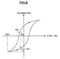
- Fig. 8 is a graph showing the level of the reference potential Vref generated by the reference cell shown in Fig. 7.
- the level of the reference potential Vref can be obtained from the cross point at which the curve of the hysteresis characteristic of the ferroelectric capacitor 14 and a load line RL1 of the parasitic capacitor Cbit of the bit line BL cross each other.
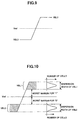
- Fig. 9 shows an ideal relationship among the reference potential output by the reference cell, the potential VBL1 of the bit line BL obtained when "1" is read from the memory cell, and the potential VBL0 of the bit line BL obtained when "0" is read from the memory cell.
- the actual level of the potential VBL1 is dispersed in a range illustrated with hatching
- the actual level of the potential VBL0 is dispersed in a range illustrated with hatching.
- the above dispersion of the potentials VBL1 and VBL0 depends on the characteristic of the memory cell.
- a more specific object of the present invention is to provide a highly reliable ferroelectric memory and a method of efficiently testing such a ferroelectric memory with ease.
- a ferroelectric memory comprising: first and second bit lines to which memory cells are connected; a first reference cell which is connected to the second bit line and outputs a reference potential to the second bit line when the memory cells connected to the first bit line are selected; a second reference cell which is connected to the first bit line and outputs the reference potential to the first bit line when the memory cells connected to the second bit line are selected; and a sense amplifier which amplifies a potential difference between the first and second bit lines and detects data output to one of the first and second bit lines from a selected memory cell.
- the ferroelectric memory includes a reference potential control circuit which controls the first and second reference cells to thereby change the reference potential.
- a ferroelectric memory comprising: memory cells; a pair of bit lines to which the memory cells are connected; and a control circuit which changes a reference cell applied to one of the pair of bit lines while data read from one of the memory cells is output to the other one of the pair of bit lines.
- a method of testing a ferroelectric memory in which data read from a memory cell is detected by a potential difference between a pair of bit lines, while one of the pair of bit lines is supplied with a reference potential and the data is read to the other one of the pair of bit lines, the method comprising the steps of: changing the reference voltages; and detecting potential margins of the pair of bit lines on the basis of data obtained while changing the reference potential.
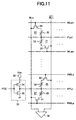
- Fig. 11 is a circuit diagram of a ferroelectric memory according to a first embodiment of the present invention.
- symbols WLon and WEen respectively denote word lines
- RPLc denotes a plate line
- 26 and 27 indicate reference cells which respectively generate the reference potential Vref
- BLn and /BLn respectively denote bit lines
- 20 and 21 respectively indicate memory cells.
- reference numbers 22 and 23 respectively indicate ferroelectric capacitors
- 24 and 25 respectively indicate nMOS transistors serving as switch elements.
- RWLo and WELe respectively denote word lines
- RPLc denotes a plate line
- 26 and 27 respectively reference cells which respectively generate the reference potential Vref
- 28 and 29 respectively indicate ferroelectric capacitors 28 and 29 having a larger area than the ferroelectric capacitors 22 and 23
- 30 and 31 respectively indicate nMOS transistors serving as switch elements.
- a reference number 32 indicates a pad to which a control potential Vex for controlling the reference potential Vref from the outside of the circuit shown in Fig. 11 is applied.
- a reference number 33 indicates a plate line drive circuit which drives the plate line RPLc. The pad 32 and the plate line drive circuit 33 forms a reference potential control circuit.
- a reference number 34 indicates a pMOS transistor such as a p-channel insulated gate field effect transistor, which is turned on/off in response to a plate line drive control signal PDC.
- the source of the pMOS transistor 34 is connected to the pad 32, and the drain thereof is connected to the plate line PLc.
- a reference number 35 indicates an nMOS transistor such as an n-channel insulated gate field effect transistor, which is turned on/off in response to the plate line drive control signal PDC.
- a reference number 36 indicates a sense amplifier, which amplifies the potential difference between the bit lines BL and /BL and thus detects data read to the bit line BL or /BL from the memory cell.
- the source of the pMOS transistor 34 is connected to the pad 32 and the source of the nMOS transistor 35 is connected to a ground.
- the pMOS transistor 34 and the nMOS transistor 35 perform a complementary operation.
- data read to the bit line BLn from a memory cell located in an odd-numbered row is compared with the reference potential Vref output to the bit line /BLn from the reference cell 26, and is thus detected.
- Data read to the bit line /BLn from a memory cell located in an even-numbered row is compared with the reference potential Vref output to the bit line BLn from the reference cell 27, and is thus detected.
- the bit line /BLn is precharged to 0 V, and is set to the high-impedance state. Then, the word line RWLo is selected, and te nMOS transistor 30 is thus turned on. Further, the plate line drive control signal PDC is set to the low level, the pMOS transistor 34 and the nMOS transistors are respectively turned on and off. Hence, the plate line RPLc is set to the control potential Vex from 0 V.
- the bit line BLn is precharged to 0 V and is set to the high-impedance state. Then, the word line RWLe is selected and the nMOS transistor 31 is thus turned on. Further, the plate line drive control signal PDC is set to the low level, and the pMOS transistor 34 and the nMOS transistor 35 are respectively turned on and off. Thus, the plate line RPLc is set to the control potential Vex from 0 V.
- Fig. 12 shows a relationship between the reference voltage Vref and the control potential Vex.
- the control potential Vex for each memory cell By changing the control potential Vex for each memory cell, the reference potential Vref is changed. Hence, at the time of reading data, the margins of the potential of the bit line to which the data is read can be inspected.
- the first embodiment of the present invention it is possible to detect products of a low reliability from those which have passed a given inspection and prevent the low-reliability products from being shipped. Hence, the shipped products are highly reliable. Further, it is possible to determine whether the products of a low reliability detected by the above have a margin failure or another factor such as a problem in the production process and to efficiently perform the failure analysis.
- the margins of the potentials of the bit lines obtained at the time of reading data can be inspected in the state of a wafer after all the circuits are formed thereon.
- the pad 32 may be connected to the VCC power supply line.
- the plate line drive circuit 33 can be used as the regular plate line drive circuit, and the chip area can efficiently be utilized.
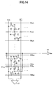
- Fig. 14 is a circuit diagram of a ferroelectric memory according to the second embodiment of the present invention.
- Reference numbers 40 and 41 respectively indicate memory cells
- 42 and 43 respectively indicate ferroelectric capacitors serving as recording media
- 44 and 45 respectively indicate nMOS transistors serving as switch elements.
- Reference numbers 46 and 47 respectively indicate reference cells which respectively output the reference potentials Vref
- 48 and 49 respectively indicate ferroelectric capacitors having a larger area than the ferroelectric capacitors 42 and 43.
- Reference numbers 50 and 51 respectively indicate nMOS transistors serving as switch elements.
- a reference number 52 is a pad to which the control voltage Vex for controlling the reference potentials Vref from the outside of the circuit shown in Fig. 14 is applied.
- Reference numbers 53 and 54 respectively indicate pMOS transistors forming precharge circuits.
- the source of the pMOS transistor 53 is connected to the pad 52, and the drain thereof is connected to a node 55.
- the gate of the pMOS transistor 53 is connected to an odd-numbered precharge control line PCLo.
- the pMOS transistor 53 is turned on/off in response to the precharge control signal transferred over the precharge control line PCLo.
- the source of the pMOS transistor 54 is connected to the pad 52, and the drain thereof is connected to a node 56.
- the gate of the pMOS transistor 54 is connected to an even-numbered precharge control line PCLe.
- the pMOS transistor 54 is turned on/off in response to the precharge control signal transferred over the precharge control line PCLe.
- the pad 52 and the pMOS transistor 53 form a reference potential control circuit associated with the bit line /BLn.
- the pad 52 and the pMOS transistor 54 form a reference potential control circuit associated withh the bit line BLn.
- a reference number 57 is a sense amplifier, which amplifies the potential difference between the bit lines BLn and /BLn and thus detect data read to the bit lines BLn and /BLn from the memory cell.
- the pMOS transistor 53 When the reference potential Vref is output to the bit line /BLn from the reference cell 46, the pMOS transistor 53 is maintained in the on state by the precharge control signal transferred over the precharge control line PCLo during the non-selected state. Hence, the node 55 is precharged to the control potential Vex. After the bit line /BLn is precharged to 0 V, it is set to the high-impedance state, and the pMOS transistor 53 is turned off by the precharge control signal transferred over the precharge control line PCLo. Then, the word line RWLo is selected and the nMOS transistor 50 is thus turned on while the plate line RPLc is maintained at 0 V.
- the pMOS transistor 54 When the reference potential Vref is output to the bit line BLn from the reference cell 47, the pMOS transistor 54 is maintained in the on state by the precharge control signal transferred over the precharge control line PCLe for the non-selected state. Then, the node 56 is precharged to the control potential Vex.
- bit line BLn is precharged to 0 V, and is set to the high-impedance state. Further, the pMOS transistor 54 is turned off by the precharge control signal transferred over the precharge control line PCLe.
- the word line RWLe is selected and the nMOS transistor 51 is turned ON while the plate line RPLc is maintained at 0 V.
- the pMOS transistor 54 When the reference voltage Vref is output to the bit line BLn from the reference cell 47, the pMOS transistor 54 is in the on state by the precharge control signal transferred over the precharge control line PCLe. Further, the node 56 is precharged to the control voltage Vex.
- the bit line BLn is precharged to 0 V, and is set to the high-impedance state. Further, the pMOS transistor 54 is turned off by the precharge control signal transferred over the precharge control line PCLe. Then, the word line RWLe is selected and the nMOS transistor 51 is turned on while the plate line RPLc is maintained at 0 V.
- the reference voltage Vref can be changed by changing the control voltage Vex. For example, as shown in Fig. 15, when Vex1 > Vex2, it is then possible to make the reference voltage Vref1 higher than the reference voltage Vref2.
- Fig. 16 shows a relationship between the control voltage Vex and the reference voltage Vref.
- the control potential Vex for each memory cell By changing the control potential Vex for each memory cell, the reference potential Vref is changed. Hence, it is possible to inspect, at the time of reading data, the margins of the potential of the bit line to which the data is read.
- the second embodiment of the present invention it is possible to detect products of a low reliability from those which have passed a given inspection and prevent the low-reliability products from being shipped. Hence, the shipped products are highly reliable. Further, it is possible to determine whether the products of a low reliability detected by the above have a margin failure or another factor such as a problem in the production process and to efficiently perform the failure analysis.
- the margins of the potentials of the bit lines obtained at the time of reading data can be inspected in the state of a wafer after all the circuits are formed thereon.
- the pad 52 may be connected to the VCC power supply line.
- the precharge circuits functioning as the reference potential control circuits can be used as the regular precharge circuits, and the chip area can efficiently be utilized.
Landscapes
- Engineering & Computer Science (AREA)
- Computer Hardware Design (AREA)
- For Increasing The Reliability Of Semiconductor Memories (AREA)
- Dram (AREA)
- Tests Of Electronic Circuits (AREA)
- Techniques For Improving Reliability Of Storages (AREA)
Applications Claiming Priority (2)
| Application Number | Priority Date | Filing Date | Title |
|---|---|---|---|
| JP23786098 | 1998-08-25 | ||
| JP23786098A JP3780713B2 (ja) | 1998-08-25 | 1998-08-25 | 強誘電体メモリ、強誘電体メモリの製造方法及び強誘電体メモリの試験方法 |
Publications (3)
| Publication Number | Publication Date |
|---|---|
| EP0986066A2 true EP0986066A2 (fr) | 2000-03-15 |
| EP0986066A3 EP0986066A3 (fr) | 2000-09-13 |
| EP0986066B1 EP0986066B1 (fr) | 2007-01-03 |
Family
ID=17021497
Family Applications (1)
| Application Number | Title | Priority Date | Filing Date |
|---|---|---|---|
| EP99108018A Expired - Lifetime EP0986066B1 (fr) | 1998-08-25 | 1999-04-23 | Mémoire ferroélectrique et méthode pour la tester |
Country Status (5)
| Country | Link |
|---|---|
| US (1) | US6229728B1 (fr) |
| EP (1) | EP0986066B1 (fr) |
| JP (1) | JP3780713B2 (fr) |
| KR (1) | KR100326991B1 (fr) |
| DE (1) | DE69934637T2 (fr) |
Cited By (2)
| Publication number | Priority date | Publication date | Assignee | Title |
|---|---|---|---|---|
| EP1143457A3 (fr) * | 2000-04-05 | 2003-07-09 | Nec Corporation | Dispositif de mémoire à semi-conducteurs et système de test et méthode de test |
| WO2004017327A3 (fr) * | 2002-08-14 | 2004-11-11 | Intel Corp | Dispositif memoire, circuits et procedes d'exploitation d'un dispositif memoire |
Families Citing this family (16)
| Publication number | Priority date | Publication date | Assignee | Title |
|---|---|---|---|---|
| JP2001093988A (ja) * | 1999-07-22 | 2001-04-06 | Sony Corp | 半導体記憶装置 |
| JP3928837B2 (ja) * | 1999-09-13 | 2007-06-13 | 株式会社ルネサステクノロジ | 半導体集積回路装置 |
| JP2001118999A (ja) * | 1999-10-15 | 2001-04-27 | Hitachi Ltd | ダイナミック型ramと半導体装置 |
| JP2001256774A (ja) * | 2000-03-09 | 2001-09-21 | Matsushita Electric Ind Co Ltd | 半導体記憶装置のデータ読み出し方法、データ書き込み方法および駆動方法 |
| WO2002052572A1 (fr) * | 2000-12-27 | 2002-07-04 | International Business Machines Corporation | Memoire ferroelectrique statique 2t-1c |
| JP2002216498A (ja) * | 2001-01-18 | 2002-08-02 | Rohm Co Ltd | 強誘電体記憶装置 |
| AU2002357606A1 (en) * | 2001-12-20 | 2003-07-09 | Matsushita Electric Industrial Co., Ltd. | Potential generating circuit, potential generating apparatus, semiconductor device using the same, and driving method thereof |
| KR100482996B1 (ko) * | 2002-08-30 | 2005-04-15 | 주식회사 하이닉스반도체 | 비휘발성 강유전체 메모리 장치 |
| US6894916B2 (en) | 2002-09-27 | 2005-05-17 | International Business Machines Corporation | Memory array employing single three-terminal non-volatile storage elements |
| US6744087B2 (en) | 2002-09-27 | 2004-06-01 | International Business Machines Corporation | Non-volatile memory using ferroelectric gate field-effect transistors |
| US6731554B1 (en) * | 2002-11-20 | 2004-05-04 | Infineon Technologies Ag | 2T2C signal margin test mode using resistive element |
| JP3806084B2 (ja) * | 2002-12-25 | 2006-08-09 | 株式会社東芝 | 強誘電体メモリ及びそのデータ読み出し方法 |
| KR100506459B1 (ko) * | 2003-09-08 | 2005-08-05 | 주식회사 하이닉스반도체 | 불휘발성 강유전체 메모리 장치 |
| JP2006024263A (ja) * | 2004-07-07 | 2006-01-26 | Seiko Epson Corp | 強誘電体記憶装置、電子機器 |
| JP4638193B2 (ja) | 2004-09-24 | 2011-02-23 | パトレネラ キャピタル リミテッド, エルエルシー | メモリ |
| WO2017145530A1 (fr) * | 2016-02-22 | 2017-08-31 | 株式会社村田製作所 | Dispositif piézoélectrique |
Family Cites Families (17)
| Publication number | Priority date | Publication date | Assignee | Title |
|---|---|---|---|---|
| US4468759A (en) * | 1982-05-03 | 1984-08-28 | Intel Corporation | Testing method and apparatus for dram |
| KR930002470B1 (ko) * | 1989-03-28 | 1993-04-02 | 가부시키가이샤 도시바 | 전기적인 독출/기록동작이 가능한 불휘발성 반도체기억장치 및 그 정보독출방법 |
| JP3110032B2 (ja) | 1990-03-30 | 2000-11-20 | 株式会社東芝 | 強誘電体メモリ |
| JPH05144296A (ja) * | 1991-11-20 | 1993-06-11 | Toshiba Corp | 半導体記憶装置の検査方法 |
| JP3191549B2 (ja) * | 1994-02-15 | 2001-07-23 | 松下電器産業株式会社 | 半導体メモリ装置 |
| JP3397452B2 (ja) * | 1994-07-06 | 2003-04-14 | 東芝マイクロエレクトロニクス株式会社 | 半導体記憶装置 |
| JP3226433B2 (ja) * | 1994-09-22 | 2001-11-05 | 松下電器産業株式会社 | 強誘電体メモリ装置 |
| JPH08203266A (ja) | 1995-01-27 | 1996-08-09 | Nec Corp | 強誘電体メモリ装置 |
| JPH097377A (ja) * | 1995-06-20 | 1997-01-10 | Sony Corp | 強誘電体記憶装置 |
| SG79200A1 (en) * | 1995-08-21 | 2001-03-20 | Matsushita Electric Industrial Co Ltd | Ferroelectric memory devices and method for testing them |
| US5680344A (en) * | 1995-09-11 | 1997-10-21 | Micron Technology, Inc. | Circuit and method of operating a ferrolectric memory in a DRAM mode |
| US5610867A (en) * | 1995-09-28 | 1997-03-11 | International Business Machines Corporation | DRAM signal margin test method |
| JPH09180467A (ja) * | 1995-10-24 | 1997-07-11 | Fujitsu Ltd | 強誘電体メモリにおけるデータの読出し方法及び強誘電体メモリ |
| US5764561A (en) * | 1995-11-16 | 1998-06-09 | Rohm Co., Ltd. | Ferroelectric memory devices and method of using ferroelectric capacitors |
| JPH10209387A (ja) * | 1996-08-22 | 1998-08-07 | Samsung Electron Co Ltd | 強誘電体メモリのセルアレイ構造及びデータ感知方法 |
| KR100268444B1 (ko) * | 1997-08-30 | 2000-10-16 | 윤종용 | 강유전체 랜덤 액세스 메모리 장치 |
| JPH11273360A (ja) * | 1998-03-17 | 1999-10-08 | Toshiba Corp | 強誘電体記憶装置 |
-
1998
- 1998-08-25 JP JP23786098A patent/JP3780713B2/ja not_active Expired - Fee Related
-
1999
- 1999-04-22 US US09/296,544 patent/US6229728B1/en not_active Expired - Lifetime
- 1999-04-23 DE DE69934637T patent/DE69934637T2/de not_active Expired - Lifetime
- 1999-04-23 EP EP99108018A patent/EP0986066B1/fr not_active Expired - Lifetime
- 1999-05-11 KR KR1019990016716A patent/KR100326991B1/ko not_active Expired - Fee Related
Cited By (7)
| Publication number | Priority date | Publication date | Assignee | Title |
|---|---|---|---|---|
| EP1143457A3 (fr) * | 2000-04-05 | 2003-07-09 | Nec Corporation | Dispositif de mémoire à semi-conducteurs et système de test et méthode de test |
| EP1408514A3 (fr) * | 2000-04-05 | 2004-04-21 | Nec Corporation | Dispositif de mémoire à semi-conducteurs et système de test et méthode de test |
| US6922799B2 (en) | 2000-04-05 | 2005-07-26 | Nec Corporation | Semiconductor memory device and testing system and testing method |
| WO2004017327A3 (fr) * | 2002-08-14 | 2004-11-11 | Intel Corp | Dispositif memoire, circuits et procedes d'exploitation d'un dispositif memoire |
| US6920060B2 (en) | 2002-08-14 | 2005-07-19 | Intel Corporation | Memory device, circuits and methods for operating a memory device |
| US7161825B2 (en) | 2002-08-14 | 2007-01-09 | Intel Corporation | Memory device, circuits and methods for operating a memory device |
| US7532498B2 (en) | 2002-08-14 | 2009-05-12 | Intel Corporation | Memory device, circuits and methods for reading a memory device |
Also Published As
| Publication number | Publication date |
|---|---|
| DE69934637D1 (de) | 2007-02-15 |
| EP0986066A3 (fr) | 2000-09-13 |
| KR100326991B1 (ko) | 2002-03-04 |
| US6229728B1 (en) | 2001-05-08 |
| EP0986066B1 (fr) | 2007-01-03 |
| JP3780713B2 (ja) | 2006-05-31 |
| KR20000016863A (ko) | 2000-03-25 |
| JP2000067597A (ja) | 2000-03-03 |
| DE69934637T2 (de) | 2007-05-03 |
Similar Documents
| Publication | Publication Date | Title |
|---|---|---|
| US5680344A (en) | Circuit and method of operating a ferrolectric memory in a DRAM mode | |
| USRE35645E (en) | Semiconductor memory device having a test mode setting circuit | |
| US5377152A (en) | Semiconductor memory and screening test method thereof | |
| US6229728B1 (en) | Ferroelectric memory and method of testing the same | |
| US6288950B1 (en) | Semiconductor memory device capable of generating offset voltage independent of bit line voltage | |
| US6055200A (en) | Variable test voltage circuits and methods for ferroelectric memory devices | |
| US5523977A (en) | Testing semiconductor memory device having test circuit | |
| US6522567B2 (en) | Semiconductor memory device and semiconductor integrated device using the same | |
| US20050195628A1 (en) | Semiconductor memory device | |
| KR100281215B1 (ko) | 강유전체 커패시터의 라이프 테스트용으로 이용가능한 단명 셀검출기를 갖는 강유전체 랜덤 액세스메모리 디바이스 및 강유전체 메모리 셀의 테스트 방법 | |
| US6118713A (en) | Device and method for stress testing a semiconduction memory | |
| KR100546417B1 (ko) | 프리차지 및 감지 증폭 스킴을 개선한 집적회로 메모리장치의 비트라인 구동회로 및 구동방법 | |
| US6512686B2 (en) | Ferroelectric storage device and test method thereof | |
| US7298655B2 (en) | Isolation control circuit and method for a memory device | |
| US7375999B2 (en) | Low equalized sense-amp for twin cell DRAMs | |
| US6385103B1 (en) | Semiconductor memory device having a circuit for testing memories | |
| US6111803A (en) | Reduced cell voltage for memory device | |
| US6950353B1 (en) | Cell data margin test with dummy cell | |
| US8050123B2 (en) | Semiconductor memory device and method of defective cell test by adjusting a bitline reference/precharge level | |
| US7330387B2 (en) | Integrated semiconductor memory device | |
| CN100452237C (zh) | 数据存取的方法和存储器件 | |
| JP2804190B2 (ja) | 半導体集積回路 | |
| JPH10233100A (ja) | 半導体メモリ装置及びその検査方法 | |
| KR960001308B1 (ko) | 반도체 메모리의 스크리닝 테스트 방법과 반도체 메모리의 제조방법 | |
| US20060187728A1 (en) | Integrated semiconductor memory |
Legal Events
| Date | Code | Title | Description |
|---|---|---|---|
| PUAI | Public reference made under article 153(3) epc to a published international application that has entered the european phase |
Free format text: ORIGINAL CODE: 0009012 |
|
| AK | Designated contracting states |
Kind code of ref document: A2 Designated state(s): DE FR |
|
| AX | Request for extension of the european patent |
Free format text: AL;LT;LV;MK;RO;SI |
|
| PUAL | Search report despatched |
Free format text: ORIGINAL CODE: 0009013 |
|
| AK | Designated contracting states |
Kind code of ref document: A3 Designated state(s): AT BE CH CY DE DK ES FI FR GB GR IE IT LI LU MC NL PT SE |
|
| AX | Request for extension of the european patent |
Free format text: AL;LT;LV;MK;RO;SI |
|
| 17P | Request for examination filed |
Effective date: 20010227 |
|
| AKX | Designation fees paid |
Free format text: DE FR |
|
| 17Q | First examination report despatched |
Effective date: 20040325 |
|
| GRAP | Despatch of communication of intention to grant a patent |
Free format text: ORIGINAL CODE: EPIDOSNIGR1 |
|
| RIN1 | Information on inventor provided before grant (corrected) |
Inventor name: YAMAZAKI, HIROKAZU, C/O FUJITSU LIMITED Inventor name: ONO,CHIKAI, C/O FUJITSU LIMITED |
|
| GRAS | Grant fee paid |
Free format text: ORIGINAL CODE: EPIDOSNIGR3 |
|
| GRAA | (expected) grant |
Free format text: ORIGINAL CODE: 0009210 |
|
| AK | Designated contracting states |
Kind code of ref document: B1 Designated state(s): DE FR |
|
| REF | Corresponds to: |
Ref document number: 69934637 Country of ref document: DE Date of ref document: 20070215 Kind code of ref document: P |
|
| ET | Fr: translation filed | ||
| PLBE | No opposition filed within time limit |
Free format text: ORIGINAL CODE: 0009261 |
|
| STAA | Information on the status of an ep patent application or granted ep patent |
Free format text: STATUS: NO OPPOSITION FILED WITHIN TIME LIMIT |
|
| 26N | No opposition filed |
Effective date: 20071005 |
|
| REG | Reference to a national code |
Ref country code: FR Ref legal event code: TP |
|
| PGFP | Annual fee paid to national office [announced via postgrant information from national office to epo] |
Ref country code: FR Payment date: 20090417 Year of fee payment: 11 |
|
| REG | Reference to a national code |
Ref country code: FR Ref legal event code: ST Effective date: 20101230 |
|
| PG25 | Lapsed in a contracting state [announced via postgrant information from national office to epo] |
Ref country code: FR Free format text: LAPSE BECAUSE OF NON-PAYMENT OF DUE FEES Effective date: 20100430 |
|
| PGFP | Annual fee paid to national office [announced via postgrant information from national office to epo] |
Ref country code: DE Payment date: 20170420 Year of fee payment: 19 |
|
| REG | Reference to a national code |
Ref country code: DE Ref legal event code: R119 Ref document number: 69934637 Country of ref document: DE |
|
| PG25 | Lapsed in a contracting state [announced via postgrant information from national office to epo] |
Ref country code: DE Free format text: LAPSE BECAUSE OF NON-PAYMENT OF DUE FEES Effective date: 20181101 |