EP0990928B1 - Filtre pour un panneau d'affichage à plasma - Google Patents
Filtre pour un panneau d'affichage à plasma Download PDFInfo
- Publication number
- EP0990928B1 EP0990928B1 EP99119251A EP99119251A EP0990928B1 EP 0990928 B1 EP0990928 B1 EP 0990928B1 EP 99119251 A EP99119251 A EP 99119251A EP 99119251 A EP99119251 A EP 99119251A EP 0990928 B1 EP0990928 B1 EP 0990928B1
- Authority
- EP
- European Patent Office
- Prior art keywords
- transparent
- film
- metallic oxide
- filter
- thickness
- Prior art date
- Legal status (The legal status is an assumption and is not a legal conclusion. Google has not performed a legal analysis and makes no representation as to the accuracy of the status listed.)
- Expired - Lifetime
Links
- 239000010410 layer Substances 0.000 claims description 93
- 229910044991 metal oxide Inorganic materials 0.000 claims description 91
- BQCADISMDOOEFD-UHFFFAOYSA-N Silver Chemical compound [Ag] BQCADISMDOOEFD-UHFFFAOYSA-N 0.000 claims description 51
- 229910052709 silver Inorganic materials 0.000 claims description 50
- 239000004332 silver Substances 0.000 claims description 50
- 239000004020 conductor Substances 0.000 claims description 41
- 230000003287 optical effect Effects 0.000 claims description 22
- 239000012790 adhesive layer Substances 0.000 claims description 21
- 238000011109 contamination Methods 0.000 claims description 18
- 239000011521 glass Substances 0.000 claims description 11
- GWEVSGVZZGPLCZ-UHFFFAOYSA-N Titan oxide Chemical compound O=[Ti]=O GWEVSGVZZGPLCZ-UHFFFAOYSA-N 0.000 claims description 8
- 229910052737 gold Inorganic materials 0.000 claims description 6
- 239000010931 gold Substances 0.000 claims description 6
- XOLBLPGZBRYERU-UHFFFAOYSA-N tin dioxide Chemical compound O=[Sn]=O XOLBLPGZBRYERU-UHFFFAOYSA-N 0.000 claims description 6
- XLYOFNOQVPJJNP-UHFFFAOYSA-N water Substances O XLYOFNOQVPJJNP-UHFFFAOYSA-N 0.000 claims description 6
- KDLHZDBZIXYQEI-UHFFFAOYSA-N Palladium Chemical compound [Pd] KDLHZDBZIXYQEI-UHFFFAOYSA-N 0.000 claims description 4
- XLOMVQKBTHCTTD-UHFFFAOYSA-N Zinc monoxide Chemical compound [Zn]=O XLOMVQKBTHCTTD-UHFFFAOYSA-N 0.000 claims description 4
- PCHJSUWPFVWCPO-UHFFFAOYSA-N gold Chemical compound [Au] PCHJSUWPFVWCPO-UHFFFAOYSA-N 0.000 claims description 4
- BASFCYQUMIYNBI-UHFFFAOYSA-N platinum Chemical compound [Pt] BASFCYQUMIYNBI-UHFFFAOYSA-N 0.000 claims description 4
- 239000004408 titanium dioxide Substances 0.000 claims description 3
- RYGMFSIKBFXOCR-UHFFFAOYSA-N Copper Chemical compound [Cu] RYGMFSIKBFXOCR-UHFFFAOYSA-N 0.000 claims description 2
- 229910052793 cadmium Inorganic materials 0.000 claims description 2
- BDOSMKKIYDKNTQ-UHFFFAOYSA-N cadmium atom Chemical compound [Cd] BDOSMKKIYDKNTQ-UHFFFAOYSA-N 0.000 claims description 2
- 229910000420 cerium oxide Inorganic materials 0.000 claims description 2
- 229910052802 copper Inorganic materials 0.000 claims description 2
- 239000010949 copper Substances 0.000 claims description 2
- 229910003437 indium oxide Inorganic materials 0.000 claims description 2
- PJXISJQVUVHSOJ-UHFFFAOYSA-N indium(iii) oxide Chemical compound [O-2].[O-2].[O-2].[In+3].[In+3] PJXISJQVUVHSOJ-UHFFFAOYSA-N 0.000 claims description 2
- WPBNNNQJVZRUHP-UHFFFAOYSA-L manganese(2+);methyl n-[[2-(methoxycarbonylcarbamothioylamino)phenyl]carbamothioyl]carbamate;n-[2-(sulfidocarbothioylamino)ethyl]carbamodithioate Chemical compound [Mn+2].[S-]C(=S)NCCNC([S-])=S.COC(=O)NC(=S)NC1=CC=CC=C1NC(=S)NC(=O)OC WPBNNNQJVZRUHP-UHFFFAOYSA-L 0.000 claims description 2
- ZKATWMILCYLAPD-UHFFFAOYSA-N niobium pentoxide Inorganic materials O=[Nb](=O)O[Nb](=O)=O ZKATWMILCYLAPD-UHFFFAOYSA-N 0.000 claims description 2
- URLJKFSTXLNXLG-UHFFFAOYSA-N niobium(5+);oxygen(2-) Chemical compound [O-2].[O-2].[O-2].[O-2].[O-2].[Nb+5].[Nb+5] URLJKFSTXLNXLG-UHFFFAOYSA-N 0.000 claims description 2
- BMMGVYCKOGBVEV-UHFFFAOYSA-N oxo(oxoceriooxy)cerium Chemical compound [Ce]=O.O=[Ce]=O BMMGVYCKOGBVEV-UHFFFAOYSA-N 0.000 claims description 2
- RVTZCBVAJQQJTK-UHFFFAOYSA-N oxygen(2-);zirconium(4+) Chemical compound [O-2].[O-2].[Zr+4] RVTZCBVAJQQJTK-UHFFFAOYSA-N 0.000 claims description 2
- 229910052763 palladium Inorganic materials 0.000 claims description 2
- 229910052697 platinum Inorganic materials 0.000 claims description 2
- 229910001887 tin oxide Inorganic materials 0.000 claims description 2
- 239000011787 zinc oxide Substances 0.000 claims description 2
- 229910001928 zirconium oxide Inorganic materials 0.000 claims description 2
- BPUBBGLMJRNUCC-UHFFFAOYSA-N oxygen(2-);tantalum(5+) Chemical compound [O-2].[O-2].[O-2].[O-2].[O-2].[Ta+5].[Ta+5] BPUBBGLMJRNUCC-UHFFFAOYSA-N 0.000 claims 1
- 229910001936 tantalum oxide Inorganic materials 0.000 claims 1
- 239000010408 film Substances 0.000 description 176
- 239000000463 material Substances 0.000 description 27
- 238000000034 method Methods 0.000 description 14
- 230000005540 biological transmission Effects 0.000 description 12
- 238000011156 evaluation Methods 0.000 description 10
- 230000008569 process Effects 0.000 description 10
- 238000005520 cutting process Methods 0.000 description 8
- 238000004544 sputter deposition Methods 0.000 description 8
- NIXOWILDQLNWCW-UHFFFAOYSA-N acrylic acid group Chemical group C(C=C)(=O)O NIXOWILDQLNWCW-UHFFFAOYSA-N 0.000 description 7
- 238000001035 drying Methods 0.000 description 7
- 238000005259 measurement Methods 0.000 description 7
- 239000000126 substance Substances 0.000 description 7
- 239000003522 acrylic cement Substances 0.000 description 6
- 239000000853 adhesive Substances 0.000 description 6
- 230000001070 adhesive effect Effects 0.000 description 6
- 230000000694 effects Effects 0.000 description 6
- 229920002284 Cellulose triacetate Polymers 0.000 description 5
- NNLVGZFZQQXQNW-ADJNRHBOSA-N [(2r,3r,4s,5r,6s)-4,5-diacetyloxy-3-[(2s,3r,4s,5r,6r)-3,4,5-triacetyloxy-6-(acetyloxymethyl)oxan-2-yl]oxy-6-[(2r,3r,4s,5r,6s)-4,5,6-triacetyloxy-2-(acetyloxymethyl)oxan-3-yl]oxyoxan-2-yl]methyl acetate Chemical compound O([C@@H]1O[C@@H]([C@H]([C@H](OC(C)=O)[C@H]1OC(C)=O)O[C@H]1[C@@H]([C@@H](OC(C)=O)[C@H](OC(C)=O)[C@@H](COC(C)=O)O1)OC(C)=O)COC(=O)C)[C@@H]1[C@@H](COC(C)=O)O[C@@H](OC(C)=O)[C@H](OC(C)=O)[C@H]1OC(C)=O NNLVGZFZQQXQNW-ADJNRHBOSA-N 0.000 description 5
- 229910052751 metal Inorganic materials 0.000 description 5
- 239000002184 metal Substances 0.000 description 5
- 239000010409 thin film Substances 0.000 description 5
- 229920002799 BoPET Polymers 0.000 description 4
- VYPSYNLAJGMNEJ-UHFFFAOYSA-N Silicium dioxide Chemical compound O=[Si]=O VYPSYNLAJGMNEJ-UHFFFAOYSA-N 0.000 description 4
- 238000000576 coating method Methods 0.000 description 4
- 239000002075 main ingredient Substances 0.000 description 4
- 238000004519 manufacturing process Methods 0.000 description 4
- -1 polyethylene terephthalate Polymers 0.000 description 4
- 229920000139 polyethylene terephthalate Polymers 0.000 description 4
- 239000005020 polyethylene terephthalate Substances 0.000 description 4
- 239000011347 resin Substances 0.000 description 4
- 229920005989 resin Polymers 0.000 description 4
- 239000013077 target material Substances 0.000 description 4
- 230000000052 comparative effect Effects 0.000 description 3
- 239000004811 fluoropolymer Substances 0.000 description 3
- 229920002313 fluoropolymer Polymers 0.000 description 3
- 238000007756 gravure coating Methods 0.000 description 3
- 238000003475 lamination Methods 0.000 description 3
- 239000000178 monomer Substances 0.000 description 3
- 239000012788 optical film Substances 0.000 description 3
- 239000007787 solid Substances 0.000 description 3
- 239000000243 solution Substances 0.000 description 3
- 238000012360 testing method Methods 0.000 description 3
- 239000011248 coating agent Substances 0.000 description 2
- 229910052681 coesite Inorganic materials 0.000 description 2
- 229910052906 cristobalite Inorganic materials 0.000 description 2
- 238000013461 design Methods 0.000 description 2
- 125000000524 functional group Chemical group 0.000 description 2
- 239000007789 gas Substances 0.000 description 2
- GKAOGPIIYCISHV-UHFFFAOYSA-N neon atom Chemical compound [Ne] GKAOGPIIYCISHV-UHFFFAOYSA-N 0.000 description 2
- 238000001579 optical reflectometry Methods 0.000 description 2
- 239000000049 pigment Substances 0.000 description 2
- 229920000058 polyacrylate Polymers 0.000 description 2
- 238000006116 polymerization reaction Methods 0.000 description 2
- 239000004926 polymethyl methacrylate Substances 0.000 description 2
- 230000005855 radiation Effects 0.000 description 2
- 239000000377 silicon dioxide Substances 0.000 description 2
- 229910052682 stishovite Inorganic materials 0.000 description 2
- 229910052905 tridymite Inorganic materials 0.000 description 2
- SMZOUWXMTYCWNB-UHFFFAOYSA-N 2-(2-methoxy-5-methylphenyl)ethanamine Chemical compound COC1=CC=C(C)C=C1CCN SMZOUWXMTYCWNB-UHFFFAOYSA-N 0.000 description 1
- OMIGHNLMNHATMP-UHFFFAOYSA-N 2-hydroxyethyl prop-2-enoate Chemical compound OCCOC(=O)C=C OMIGHNLMNHATMP-UHFFFAOYSA-N 0.000 description 1
- 239000004925 Acrylic resin Substances 0.000 description 1
- 229920000178 Acrylic resin Polymers 0.000 description 1
- 229920006353 Acrylite® Polymers 0.000 description 1
- 239000004971 Cross linker Substances 0.000 description 1
- KRHYYFGTRYWZRS-UHFFFAOYSA-M Fluoride anion Chemical compound [F-] KRHYYFGTRYWZRS-UHFFFAOYSA-M 0.000 description 1
- CERQOIWHTDAKMF-UHFFFAOYSA-N Methacrylic acid Chemical compound CC(=C)C(O)=O CERQOIWHTDAKMF-UHFFFAOYSA-N 0.000 description 1
- 206010034960 Photophobia Diseases 0.000 description 1
- 239000004696 Poly ether ether ketone Substances 0.000 description 1
- 239000004695 Polyether sulfone Substances 0.000 description 1
- 229920000297 Rayon Polymers 0.000 description 1
- XUIMIQQOPSSXEZ-UHFFFAOYSA-N Silicon Chemical compound [Si] XUIMIQQOPSSXEZ-UHFFFAOYSA-N 0.000 description 1
- 238000003848 UV Light-Curing Methods 0.000 description 1
- 230000002745 absorbent Effects 0.000 description 1
- 239000002250 absorbent Substances 0.000 description 1
- 239000006096 absorbing agent Substances 0.000 description 1
- 229920000122 acrylonitrile butadiene styrene Polymers 0.000 description 1
- 239000000654 additive Substances 0.000 description 1
- QVGXLLKOCUKJST-UHFFFAOYSA-N atomic oxygen Chemical compound [O] QVGXLLKOCUKJST-UHFFFAOYSA-N 0.000 description 1
- 230000004888 barrier function Effects 0.000 description 1
- 229910000416 bismuth oxide Inorganic materials 0.000 description 1
- WUKWITHWXAAZEY-UHFFFAOYSA-L calcium difluoride Chemical compound [F-].[F-].[Ca+2] WUKWITHWXAAZEY-UHFFFAOYSA-L 0.000 description 1
- 229910001634 calcium fluoride Inorganic materials 0.000 description 1
- 239000003795 chemical substances by application Substances 0.000 description 1
- 239000002131 composite material Substances 0.000 description 1
- 239000000470 constituent Substances 0.000 description 1
- 230000001419 dependent effect Effects 0.000 description 1
- 238000000151 deposition Methods 0.000 description 1
- 230000008021 deposition Effects 0.000 description 1
- 230000006866 deterioration Effects 0.000 description 1
- TYIXMATWDRGMPF-UHFFFAOYSA-N dibismuth;oxygen(2-) Chemical compound [O-2].[O-2].[O-2].[Bi+3].[Bi+3] TYIXMATWDRGMPF-UHFFFAOYSA-N 0.000 description 1
- KPUWHANPEXNPJT-UHFFFAOYSA-N disiloxane Chemical class [SiH3]O[SiH3] KPUWHANPEXNPJT-UHFFFAOYSA-N 0.000 description 1
- 238000007720 emulsion polymerization reaction Methods 0.000 description 1
- IPZIVCLZBFDXTA-UHFFFAOYSA-N ethyl n-prop-2-enoylcarbamate Chemical class CCOC(=O)NC(=O)C=C IPZIVCLZBFDXTA-UHFFFAOYSA-N 0.000 description 1
- 238000010528 free radical solution polymerization reaction Methods 0.000 description 1
- 230000009477 glass transition Effects 0.000 description 1
- 239000011261 inert gas Substances 0.000 description 1
- 238000007733 ion plating Methods 0.000 description 1
- 150000002500 ions Chemical class 0.000 description 1
- 238000010030 laminating Methods 0.000 description 1
- 229910001635 magnesium fluoride Inorganic materials 0.000 description 1
- 238000001755 magnetron sputter deposition Methods 0.000 description 1
- 150000002739 metals Chemical class 0.000 description 1
- 238000013508 migration Methods 0.000 description 1
- 230000005012 migration Effects 0.000 description 1
- 239000000203 mixture Substances 0.000 description 1
- 238000012986 modification Methods 0.000 description 1
- 230000004048 modification Effects 0.000 description 1
- 229910052961 molybdenite Inorganic materials 0.000 description 1
- CWQXQMHSOZUFJS-UHFFFAOYSA-N molybdenum disulfide Chemical compound S=[Mo]=S CWQXQMHSOZUFJS-UHFFFAOYSA-N 0.000 description 1
- 229910052982 molybdenum disulfide Inorganic materials 0.000 description 1
- 229910052754 neon Inorganic materials 0.000 description 1
- 239000001301 oxygen Substances 0.000 description 1
- 229910052760 oxygen Inorganic materials 0.000 description 1
- 229920003023 plastic Polymers 0.000 description 1
- 229920003207 poly(ethylene-2,6-naphthalate) Polymers 0.000 description 1
- 229920003229 poly(methyl methacrylate) Polymers 0.000 description 1
- 229920001230 polyarylate Polymers 0.000 description 1
- 239000004417 polycarbonate Substances 0.000 description 1
- 229920000515 polycarbonate Polymers 0.000 description 1
- 239000004431 polycarbonate resin Substances 0.000 description 1
- 229920005668 polycarbonate resin Polymers 0.000 description 1
- 229920000728 polyester Polymers 0.000 description 1
- 229920006267 polyester film Polymers 0.000 description 1
- 229920006393 polyether sulfone Polymers 0.000 description 1
- 229920002530 polyetherether ketone Polymers 0.000 description 1
- 239000011112 polyethylene naphthalate Substances 0.000 description 1
- 239000002685 polymerization catalyst Substances 0.000 description 1
- 239000011241 protective layer Substances 0.000 description 1
- 239000005871 repellent Substances 0.000 description 1
- 238000012827 research and development Methods 0.000 description 1
- 229910052710 silicon Inorganic materials 0.000 description 1
- 239000010703 silicon Substances 0.000 description 1
- 239000006104 solid solution Substances 0.000 description 1
- 230000003746 surface roughness Effects 0.000 description 1
- 238000010557 suspension polymerization reaction Methods 0.000 description 1
- 229920001187 thermosetting polymer Polymers 0.000 description 1
- 230000007704 transition Effects 0.000 description 1
- 238000002834 transmittance Methods 0.000 description 1
- 238000001771 vacuum deposition Methods 0.000 description 1
- 230000037303 wrinkles Effects 0.000 description 1
Images

Classifications
-
- C—CHEMISTRY; METALLURGY
- C03—GLASS; MINERAL OR SLAG WOOL
- C03C—CHEMICAL COMPOSITION OF GLASSES, GLAZES OR VITREOUS ENAMELS; SURFACE TREATMENT OF GLASS; SURFACE TREATMENT OF FIBRES OR FILAMENTS MADE FROM GLASS, MINERALS OR SLAGS; JOINING GLASS TO GLASS OR OTHER MATERIALS
- C03C17/00—Surface treatment of glass, not in the form of fibres or filaments, by coating
- C03C17/34—Surface treatment of glass, not in the form of fibres or filaments, by coating with at least two coatings having different compositions
- C03C17/36—Surface treatment of glass, not in the form of fibres or filaments, by coating with at least two coatings having different compositions at least one coating being a metal
- C03C17/3602—Surface treatment of glass, not in the form of fibres or filaments, by coating with at least two coatings having different compositions at least one coating being a metal the metal being present as a layer
- C03C17/3613—Coatings of type glass/inorganic compound/metal/inorganic compound/metal/other
-
- C—CHEMISTRY; METALLURGY
- C03—GLASS; MINERAL OR SLAG WOOL
- C03C—CHEMICAL COMPOSITION OF GLASSES, GLAZES OR VITREOUS ENAMELS; SURFACE TREATMENT OF GLASS; SURFACE TREATMENT OF FIBRES OR FILAMENTS MADE FROM GLASS, MINERALS OR SLAGS; JOINING GLASS TO GLASS OR OTHER MATERIALS
- C03C17/00—Surface treatment of glass, not in the form of fibres or filaments, by coating
- C03C17/34—Surface treatment of glass, not in the form of fibres or filaments, by coating with at least two coatings having different compositions
- C03C17/36—Surface treatment of glass, not in the form of fibres or filaments, by coating with at least two coatings having different compositions at least one coating being a metal
- C03C17/3602—Surface treatment of glass, not in the form of fibres or filaments, by coating with at least two coatings having different compositions at least one coating being a metal the metal being present as a layer
- C03C17/3639—Multilayers containing at least two functional metal layers
-
- C—CHEMISTRY; METALLURGY
- C03—GLASS; MINERAL OR SLAG WOOL
- C03C—CHEMICAL COMPOSITION OF GLASSES, GLAZES OR VITREOUS ENAMELS; SURFACE TREATMENT OF GLASS; SURFACE TREATMENT OF FIBRES OR FILAMENTS MADE FROM GLASS, MINERALS OR SLAGS; JOINING GLASS TO GLASS OR OTHER MATERIALS
- C03C17/00—Surface treatment of glass, not in the form of fibres or filaments, by coating
- C03C17/34—Surface treatment of glass, not in the form of fibres or filaments, by coating with at least two coatings having different compositions
- C03C17/36—Surface treatment of glass, not in the form of fibres or filaments, by coating with at least two coatings having different compositions at least one coating being a metal
- C03C17/3602—Surface treatment of glass, not in the form of fibres or filaments, by coating with at least two coatings having different compositions at least one coating being a metal the metal being present as a layer
- C03C17/3644—Surface treatment of glass, not in the form of fibres or filaments, by coating with at least two coatings having different compositions at least one coating being a metal the metal being present as a layer the metal being silver
-
- C—CHEMISTRY; METALLURGY
- C03—GLASS; MINERAL OR SLAG WOOL
- C03C—CHEMICAL COMPOSITION OF GLASSES, GLAZES OR VITREOUS ENAMELS; SURFACE TREATMENT OF GLASS; SURFACE TREATMENT OF FIBRES OR FILAMENTS MADE FROM GLASS, MINERALS OR SLAGS; JOINING GLASS TO GLASS OR OTHER MATERIALS
- C03C17/00—Surface treatment of glass, not in the form of fibres or filaments, by coating
- C03C17/34—Surface treatment of glass, not in the form of fibres or filaments, by coating with at least two coatings having different compositions
- C03C17/36—Surface treatment of glass, not in the form of fibres or filaments, by coating with at least two coatings having different compositions at least one coating being a metal
- C03C17/3602—Surface treatment of glass, not in the form of fibres or filaments, by coating with at least two coatings having different compositions at least one coating being a metal the metal being present as a layer
- C03C17/3657—Surface treatment of glass, not in the form of fibres or filaments, by coating with at least two coatings having different compositions at least one coating being a metal the metal being present as a layer the multilayer coating having optical properties
-
- C—CHEMISTRY; METALLURGY
- C03—GLASS; MINERAL OR SLAG WOOL
- C03C—CHEMICAL COMPOSITION OF GLASSES, GLAZES OR VITREOUS ENAMELS; SURFACE TREATMENT OF GLASS; SURFACE TREATMENT OF FIBRES OR FILAMENTS MADE FROM GLASS, MINERALS OR SLAGS; JOINING GLASS TO GLASS OR OTHER MATERIALS
- C03C17/00—Surface treatment of glass, not in the form of fibres or filaments, by coating
- C03C17/34—Surface treatment of glass, not in the form of fibres or filaments, by coating with at least two coatings having different compositions
- C03C17/36—Surface treatment of glass, not in the form of fibres or filaments, by coating with at least two coatings having different compositions at least one coating being a metal
- C03C17/3602—Surface treatment of glass, not in the form of fibres or filaments, by coating with at least two coatings having different compositions at least one coating being a metal the metal being present as a layer
- C03C17/3668—Surface treatment of glass, not in the form of fibres or filaments, by coating with at least two coatings having different compositions at least one coating being a metal the metal being present as a layer the multilayer coating having electrical properties
- C03C17/3676—Surface treatment of glass, not in the form of fibres or filaments, by coating with at least two coatings having different compositions at least one coating being a metal the metal being present as a layer the multilayer coating having electrical properties specially adapted for use as electromagnetic shield
-
- G—PHYSICS
- G02—OPTICS
- G02B—OPTICAL ELEMENTS, SYSTEMS OR APPARATUS
- G02B5/00—Optical elements other than lenses
- G02B5/20—Filters
- G02B5/204—Filters in which spectral selection is performed by means of a conductive grid or array, e.g. frequency selective surfaces
Definitions
- the present invention relates to a filter for a plasma display panel (hereinafter abbreviated to 'PDP') disposed on the front surface of a PDP in order to simultaneously cut electromagnetic waves and near infrared rays generated from the PDP, and a PDP display unit with this filter stuck thereto.
- 'PDP' plasma display panel
- a PDP is charged with gas mainly consisting of inert gas, particularly neon.
- gas mainly consisting of inert gas, particularly neon.
- electrons discharged from a cathode are accelerated so as to have a collision with gas molecules and make their way to an anode while being exited or ionized.
- Positive ions generated in the anode also collide against the cathode so that electrons are emitted so as to commence electrical discharge.
- electromagnetic waves and near infrared rays are emitted with the transition procedure of neon atoms.
- the emitted near infrared rays have a wavelength in a range of from 850 to 1,200 nm.
- the light sensitivities of remote controllers for household appliances, KARAOKE equipments, audio/video systems, etc. are in a range of from 700 to 1,300 nm. Therefore, there has arisen a problem that the near infrared rays emitted from the PDP cause erroneous operations in the remote controllers.
- the near infrared rays are generated on the principle of the PDP, and they cannot be prevented in the PDP itself.
- US-A-5 071 206 discloses a transparent heat reflecting filter to be used therewith in order to reflect infrared radiation and transmit the desired visible radiation.
- the filter has a laminate structure comprising alternate transparent dielectric layers and transparent silver metal layers with normally 3 to 5 transparent metal layers being preferred.
- the thickness of the various layers in the filter are controlled to achieve an optimum balance between desired infrared reflectance and visible light transmittance.
- the thickness of the dielectric layers being dependent on the index of refraction and the middle metal layers being formed to be about 5% to 15% thicker than each of the outer layers.
- the above-mentioned mesh type can obtain a low resistance value, but it has drawbacks that a filter for cutting near infrared rays is necessary otherwise, and a moire phenomenon is produced due to the display pattern intervals of the PDP so that the display quality deteriorates.
- the filter produced by a dry process represented by the sputtering process no moire phenomenon is seen, but there has been no filter which can satisfy at the same time the properties of low resistance, visible light transparency, cutting of near infrared rays of 850 to 1,200 nm, and low visible light reflection, and which can be formed in a comparatively simple laminated configuration.
- the filter is set on the front side of the PDP through an air layer in such a method, the visibility is reduced and the features of the PDP, that is, lightness in weight and thinness in thickness, are spoiled.
- Prior art EP-A-0 810 452 discloses a filter for a display of the type comprising a laminate structure formed by laminating transparent high-refractive-index film layers and metal film layers consisting of silver, 3 or more times onto a transparent base.
- the filter also comprises an additional top layer such as a transparent protective layer, transparent antireflection layer and the like.
- the optical design of this filter takes into consideration this additional top layer such that the visible-light reflectivity is suppressed to 2% or less.
- the present invention achieves its task by providing a filter for a plasma display comprising the features set out in claim 1.
- a filter for a plasma display panel is constituted by a laminated body in which n units 3 ⁇ n ⁇ 10 each consisting of a metallic oxide film and a silver transparent electric-conductor film are successively laminated unit after unit on a surface of a transparent film base, and a metallic oxide film is formed on the units as an outermost layer of the laminated body.
- Each metallic oxide film has optical transparency of a refractive index of 1.5 to 2.7
- each silver transparent electric-conductor film has a thickness set substantially to a fixed value in a range of from 5 to 20 nm.
- Each of the metallic oxide film put directly on the surface of the base and the outermost-layer metallic oxide film has a thickness 5/2 (1 ⁇ 0.15) times as large as the thickness of each silver transparent electric-conductor film.
- Each of the other metallic oxide films located halfway between the metallic oxide film put directly on the surface of the base and the outermost-layer metallic oxide film has a thickness 5 (1 ⁇ 0.15) times as large as the thickness of each silver transparent electric-conductor film.
- the objects of the present invention can be attained by the laminated body in which an anti-reflection and anti-contamination layer 0.001 to 1 ⁇ m thick is further formed on the hard coat layer.
- the hard coat layer is a coating film having a refractive index of 1.45 or less, a thickness of 0.05 to 10 ⁇ m, and an angle of contact with water of 90° or more.
- the objects are attained by the laminated body in which a film in which a hard coat layer, an anti-reflection layer and an anti-contamination layer are formed on one surface of another transparent film base is prepared, and the film is stuck to the surface of the outermost metallic oxide film through a transparent adhesive layer formed on the other surface of the other transparent film base.
- an undercoat layer with a refractivity of 1.5 or less and a thickness of 0.05 to 1 ⁇ m is formed between the surface of the transparent film base and the metallic oxide film provided on the surface of the film base.
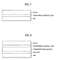
- the laminated body in which a transparent adhesive layer 10 to 500 ⁇ m thick is formed on the back surface of the transparent film base is stuck to a front display glass portion of a PDP through the transparent adhesive layer (Fig. 7), or the laminated body is stuck, through the transparent adhesive layer, to the other surface side of a transparent molded body which is attached at its on surface side to the front side of a PDP through an air layer (Fig. 8).
- the expected objects of electromagnetic wave shielding properties, near infrared ray cutting properties and low visible light reflection properties necessary to a PDP can be attained by a comparatively simple laminated configuration.
- PDP display unit having a PDP front filter which is superior in visibility, light in weight and thin in thickness.
- a PDP filter according to the present invention will be specifically described below, with reference to Figs. 1 and 2.
- metallic oxide films (2A, 2B and 2C) and silver transparent electric-conductor films (3A, 3B and 3C) are successively and alternatively laminated on the surface of a transparent film base 1 (Fig. 1 shows an example of three units) so that every unit is constituted by a metallic oxide film and a silver transparent electric-conductor film, a metallic oxide film 2D being formed in the outermost layer.
- Each of the above-mentioned metallic oxide films is a film having optical transparency of a refractive index in a range of from 1.5 to 2.7.
- the thickness of each silver transparent electric-conductor film is set substantially to a fixed value in a range of from 5 to 20 nm.
- design is made so that each of the thickness of the metallic oxide film on the base surface and the thickness of the outermost metallic oxide film (2A, 2D) is 5/2 (1 ⁇ 0.15) times as large as the thickness of each silver transparent electric-conductor film, while the thickness of each of the other metallic oxide films located halfway (2B, 2C) is 5 (1 ⁇ 0.15) times as large as the thickness of each silver transparent electric-conductor film.
- Fig. 1 shows an example in which a hard coat layer 4 and an anti-reflection and anti-contamination layer 5 are further formed on the surface of the outermost metallic oxide film 2D, and a transparent adhesive layer is formed on the back surface of the transparent film base 1.
- Fig. 2 illustrates another embodiment, showing an example of the PDP filter in which an undercoat layer 9 with a refractive index of 1.5 or less and a thickness of 0.05 to 1 ⁇ m is formed between the surface of the transparent film base 1 and the metallic oxide film 2A provided on the surface thereof, while a film in which a hard coat layer 4, an anti-reflection layer 7 and an anti-contamination layer 8 are successively formed on one side of another transparent film base 11 is prepared, and the film is stuck to the surface of the outermost metallic oxide film 2D through a transparent adhesive layer 61 formed on the other side of the base 11.
- the transparent film base used in the present invention one having transparency in the visible light range is available if its surface is smooth to some extent.
- polyethylene terephthalate, triacetyl cellulose, polyethylene naphthalate, polyether sulfone, polycarbonate, polyarylate, polyether ether ketone, etc. are preferable.
- a film base having a thickness of 10 to 250 ⁇ m is usually used.
- a polymeric film may be used as it is without any treatment, as the film base, it may be subject to a hard coating treatment for giving mar-proof property to its one or both sides.
- the treatment may be of the UV-curing type or of the thermosetting type, and the thickness is preferably in a range of from 1 to 10 ⁇ m. The mar-proof effect is lowered if the thickness is less than 1 ⁇ m. On the other hand, a crack is apt to appear if the thickness exceeds 10 ⁇ m.
- pigment for adjusting the color of visible light may be mixed into the film base, or coated on the film base.
- the transparent molded body examples include transparent plastic plates of acrylic resin such as poly methyl methacrylate, polycarbonate resin, ABS resin, etc., and glass plates.
- the molded body is not limited particularly to those mentioned above, so long as it has a transparency, a certain measure of mechanical strength and heat resistance.
- the thickness thereof is in a range of from 1 to 10 mm, preferably from 2 to 5 mm.
- pigment for adjusting the color of visible light may be mixed into the inside of the transparent molded body, or coated on the surface thereof.
- a hard coat layer, an anti-reflection layer, an anti-glare layer and so on may be formed directly on the PDP-side surface of the transparent molded body, or a transparent film base of which these layers are once formed may be stuck to the PDP-side surface.
- the refractive index of the thin films is in a range of from 1.5 to 2.7. If the refractive index is less than 1.5, it is necessary to increase the thickness of the metallic oxide films, with the result that cracks are apt to appear when the metallic oxide films are multilayered. On the other hand, if the refractive index is beyond 2.7, the difference in refractive index between the outermost metallic oxide film and the air becomes too great to suppress the visible light reflectance to a low value.
- a single metallic oxide or a mixture of metallic oxides may be available. Further, more preferable is a material which has an effect to prevent migration of silver, or an effect of barrier to water and oxygen.
- the metallic oxide materials are oxide which has indium oxide as the main ingredient and contains a small amount of titanium dioxide, tin oxide, cerium oxide; titanium dioxide; zirconium oxide; bismuth oxide; niobium pentoxide; zinc oxide; etc.
- These thin film layers can be provided in a vacuum dry process such as sputtering, vacuum deposition, ion plating, or the like.
- the thickness of the metallic oxide films is preferably within a range of from 18 to 100 nm, and the film thickness providing the optimum optical properties is decided by the refractive index thereof, the thickness of the silver transparent electric-conductor films, the total number of layers, and so on.
- the material of the silver transparent electric-conductor films consists of silver of 90 weight % or more and one or more elements selected from gold, copper, palladium, platinum, manganese, and cadmium. It is preferable to use a material containing a solid solution of silver of 90 to 99 weight % and the above-mentioned metals of 1 to 10 weight % in view of preventing silver from deterioration. If gold mixed therein is not less than 10 weight %, the specific resistance increases so that it is difficult to obtain a low resistance value. On the other hand, if gold is not more 1 weight %, silver is apt to deteriorate.
- the means for forming the silver transparent electric-conductor films As the means for forming the silver transparent electric-conductor films, a vacuum dry process such as sputtering or the like is used.
- the thickness of the silver transparent electric-conductor films is preferably in a range of from 5 to 20 nm, and more preferably in a range of from 9 to 17 nm.
- Target Properties of PDP Filter Item Target Properties Surface Resistance Value 2 ⁇ / ⁇ or less Visible Light Transmission at 550nm 40% or more IR Cut Ratio at 850-1200 nm 95% or more Visible Light Reflectance at 550nm 3% or less
- the present inventors repeated earnest examination on means for satisfying such required properties in a dry process on a transparent film base with a comparatively simple laminated configuration.
- the present inventors have found that a filter which does not require an IR absorbent and which is superior in optical properties while having a low resistance value can be attained in a comparatively simple laminated configuration when the following conditions are satisfied by a laminated body in which a metallic oxide film, a silver transparent electric-conductor film, a metallic oxide film, a silver transparent electric-conductor film, and a metallic oxide film are laminated successively and alternately in multi-layers on a transparent film base, that is, a laminated body expressed by the expression of transparent film base/(metallic oxide film/silver transparent electric-conductor film)n/metallic oxide film.
- the laminated body has a lamination of a transparent film base 1/a metallic oxide film 2A/silver transparent electric-conductor film 3A/the same 2B/the same 3B/the same 2C/the same 3C/a metallic oxide film 2D.
- the silver transparent electric-conductor films (3A, 3B and 3C) are set to be 13 nm thick
- the metallic oxide films (2A and 2D) are 32.5 nm thick
- the metallic oxide films (2B and 2C) are 65 nm thick. Then the optical properties in Table 1 can be satisfied.
- the laminated body has a lamination of 1/2A/3A/2B/3B/2C/3C/2D/3D/2E.
- the silver transparent electric-conductor films (3A, 3B, 3C and 3D) are set to be 12 nm thick
- the metallic oxide films (2A and 2E) are 30 nm thick
- the metallic oxide films (2B, 2C and 2D) are 60 nm thick.
- silver transparent electric-conductor films (3A to 3E) are set to be 11 nm thick
- metallic oxide films (2A and 2F) are 27.5 nm thick
- metallic oxide films (2B, 2C, 2D and 2E) are 55 nm thick.
- the tolerance between 5/2 times and 5 times which are setting conditions for the thickness of metallic oxide films depends on the refractive index of the metallic oxide films.
- the optimum refractive index and the thickness of metallic oxide films are set under the condition of n ⁇ 3.
- n ⁇ 3 the surface resistance value can be reduced by increasing the thickness of each silver transparent electric-conductor film, while the optical properties cannot be satisfied.
- n>10 there are combinations satisfying the properties in Table 1, but the configuration itself becomes complicated, so that the objects of the present invention cannot be attained in a comparatively simple configuration which is intended by the invention.
- the hard coat layer 4 is formed in order to prevent the laminated body from being injured, because the laminated body is stuck directly to the PDP front display portion and there is therefore a high possibility that a human may touch the laminated body.
- the refractive index of the hard coat layer is 1.45 or less, the property of surface hard coat can be given without reducing the optical properties, particularly without reducing the reflection properties from the innermost metallic oxide film to the outermost metallic oxide film.
- the hard coat layer has an angle of contact with water of 90 ° or more because the hard coat layer can also has an anti-contamination property.
- the film thickness is preferably in a range of from 0.05 to 10 ⁇ m, more preferably in a range of from 0.1 to 6 ⁇ m.
- thermosetting-type SiO 2 materials thermosetting-type fluoro polymer materials, etc. are preferable in hardness, but the hard coat materials are not limited thereto.
- an anti-reflection and anti-contamination layer 5 may be formed though it is not required to be formed.
- the thickness is preferably set to be in a range of from 0.05 to 10 ⁇ m, more preferably from 0.1 to 6 ⁇ m.
- An anti-reflection and anti-contamination layer 5 may be formed on this surface in order to improve the reflection properties.
- an optical film of low-refractive fluororesin, MgF 2 , CaF 2 , or the like may be formed in a dry process such as a coating method, a sputtering method or the like.
- the thickness of the optical film is preferably set to be in a range of from about 0.001 to 1 ⁇ m.
- a film in which a hard coat layer 4, an anti-reflection layer 7 and an anti-contamination layer 8 are formed on one side of another transparent film base 11 is prepared, and the film is stuck to the surface of the outermost metallic oxide film through a transparent adhesive layer 61 formed on the other side of the base 11.
- any material if it can be used as the transparent film base 1, may be used as the transparent film base 11 without limitation.
- polyester film or triacetyl cellulose film is used.
- a high hard coat agent is generally used, and it is preferable to use a material selected from UV-curing-type acryl urethane derivatives, thermosetting-type siloxane derivatives, or the like, and with a thickness in a range of from about 1 to 10 m.
- the anti-reflection layer and the anti-contamination layer may be replaced by one layer formed of a material having both the above-mentioned anti-reflection property and anti-contamination property.
- a material of water-repellent fluororesin, MoS 2 or the like may be subjected to a dry process such as a thin layer coating process, a sputtering process or the like, so as to form an anti-contamination layer on an anti-reflection layer constituted by a multilayer film of a high-refractive film and a low-refractive film formed by a method such as sputtering deposition or the like.
- an undercoat layer 9 with a refractive index of 1.5 or less and a thickness of 0.05 to 1 ⁇ m is formed between the surface of the transparent film base and the innermost metallic oxide film, there are an effect that the adhesion between the metallic oxide film and the film base can be improved, and an effect that the visible light reflectance of the laminated body as a whole is further reduced.
- the material of the undercoat layer UV-curing-type low-refractive fluoro polymer to which a functional group is introduced to improve the adhesion, UV-curing-type low-refractive inorganic coat material, etc. are available.
- the elastic modulus is preferably in a range of from 1 ⁇ 10E 5 to 1 ⁇ 10E 7 dyn/cm 2 , and the thickness is preferably in a range of from 10 to 500 ⁇ m, more preferably from 25 to 300 ⁇ m.
- materials thereof include acrylic adhesive, rubber adhesive, polyester adhesive, etc. Particularly it is preferable to use an acrylic adhesive.
- one or more kinds of (meth)acrylate alkyl esters having a glass transition point not higher than -10°C after being polymerized, as principal monomers for giving moderate wettability and plasticity as an adhesive, and in accordance with necessity functional-group containing monomers such as acrylic acid, methacrylic acid, 2-hydroxyethyl acrylate, and so on, and other copolymerizable monomers are polymerized in a process such as a solution polymerization process, an emulsion polymerization process, a self-polymerization process (particularly a polymerization process by using ultraviolet rays), a suspension polymerization process, etc., by using a suitable polymerization catalyst.
- the acrylic polymer may be of a thermo crosslinkable type, a photo (ultraviolet rays or electron rays) crosslinkable type, or the like.
- the transparent adhesive layer having the above-mentioned properties is used, a swell in the PDP glass surface is absorbed so as to improve the sticking while the film is stuck directly to the PDP front display glass.
- a swell in the PDP glass surface is absorbed so as to improve the sticking while the film is stuck directly to the PDP front display glass.
- the adhesive thickness is reduced for a moment, the adhesive restores itself before long so that the film recovers its original smooth surface as if nothing had happened.
- UV-curing-type hard coat resin (having as its main ingredient, the trade name UNIDIC 17-813 made by DAINIPPON INK AND CHEMICALS, INCORPORATED) was applied to be 5 ⁇ m thick on one side of a transparent polyethylene terephthalate (PET) film 125 ⁇ m thick.
- PET polyethylene terephthalate
- thin films were formed successively on the hard coat (HC) side in the order of a metallic oxide film, a silver transparent electric-conductor film, and a metallic oxide film, in a DC magnetron sputtering process.
- the visible light transmission at 550 nm of the transparent film base with the HC was 89%.
- TiO 2 was used as target material for forming the metallic oxide films
- Ag-5 weight% Au was used as target material for forming the silver transparent electric-conductor films.
- the film thickness was measured by a working curve of film-forming speed by using a surface roughness tester (DEKTAK3) and precision measurement by using a transmission-type electron microscope, upon each film attached to a thick film.
- a tester made by MITSUBISHI PETROCHEMICAL CO., LTD. was used.
- optical properties were measured by using U-3410 made by HITACHI, LTD.
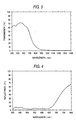
- Figs. 3 and 4 optical measurement charts about the sample (1) of the produced filters are shown in Figs. 3 and 4. According to Fig. 3, it is seen that high transmission could be obtained in the visible light area, and most of near infrared rays not less than 800 nm were cut. According to Fig. 4, it is understood that reflectance was low all over the visible light area.
- Example 2 Although respective materials and a production method were similar to those in Example 1, the thickness of metallic oxide films was set to the following values which were departed from the scope of the present invention. Two kinds of laminated body samples (4) and (5) were produced thus, and evaluation was performed in the same manner as that in Example 1.
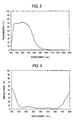
- Figs. 5 and 6 the optical measurement charts about the produced sample (4) are shown in Figs. 5 and 6. According to Fig. 5, it is seen that the transmission of blue light deteriorates, and the cutting of near infrared rays not less than 800 nm are insufficient. In addition, according to Fig. 6, it is understood that the reflectance of blue is high.
- UV-curing-type low-refractive fluoro polymer (the trade name JM5010, made by NIPPON SYNTHETIC CHEMICAL INDUSTRY CO., LTD.) was applied by gravure coating onto an HC of a transparent PET film 125 ⁇ m thick similar to that in Example 1, and cured by ultraviolet irradiation at 300 mJ/cm 2 for 3 minutes, so that an undercoat layer 0.15 ⁇ m thick was formed.
- the refractive index of this layer was 1.41, and the material used therefor had no slipperiness in order to improve the adherence between the HC of the transparent film base and the metallic oxide film formed thereon.
- an SiO 2 hard coat material (the trade name LR201, made by NISSAN CHEMICAL INDUSTRIES, LTD.) with a refractive index of 1.36 was formed as a hard coat layer on the above-mentioned outermost metallic oxide film by gravure coating, and thereafter cured at 150°C for 5 minutes.
- the thus obtained hard coat layer was 5 ⁇ m thick, and the angle of contact with water was 104 degrees.
- acrylic adhesive solution with a solids content of 20 weight % was coated on the back surface of the above-mentioned transparent film base, and dried at 150°C for 5 minutes, thereby forming a transparent adhesive layer with a thickness of 50 ⁇ m and an elasticity modulus of 1.8 ⁇ 10E 6 dyn/cm 2 .
- a laminated body sample (6) was produced thus.
- This sample (6) and another sample in which the same sample (6) was stuck to a PDP front display glass portion by a roll laminator were prepared as evaluation samples.
- the results of evaluation are shown in Table 4.
- the sample (6) provided superior results in electromagnetic wave shield properties, near infrared ray cut properties, and low visible light reflection properties, and it was possible to obtain a PDP front filter superior in mar-proof, superior in visibility, and having both thinness and lightness in weight.
- An undercoat layer 0.15 ⁇ m thick similar to that in Example 1 was formed on one side of a transparent PET film 125 ⁇ m thick.
- a laminated body was obtained in the same manner as that in Example 1, except that on this undercoat layer, In 2 O 3 -10 weight% SnO 2 was used as target material for forming metallic oxide films, and Ag-3 weight% Au was used as target material for forming silver transparent electric-conductor films. Then the refractive index of In 2 O 3 -10 weight% SnO 2 was 2.0.
- UV-curing-type hard coat (having as its main ingredient, the trade name UNIDIC 17-813, made by DAINIPPON INK AND CHEMICALS, INCORPORATED) with a refractive index of 1.55 was applied onto the outermost metallic oxide film in a fountain reverse process, and solidified by ultraviolet irradiation at 300 mJ/cm 2 for 3 minutes, so as to form a hard coat layer 5 ⁇ m thick.
- an organic fluoride anti-reflection and anti-contamination material (the trade name JM5025, made by NIPPON SYNTHETIC CHEMICAL INDUSTRY CO., LTD.) was applied onto the hard coat layer by gravure coating, and irradiated by ultraviolet rays at 300 mJ/cm 2 for 3 minutes so as to form an anti-reflection and anti-contamination layer 0.15 ⁇ m thick.
- acrylic adhesive solution with a solids content of 20 weight % was coated on the back surface of the above-mentioned transparent film base, and dried at 150°C for 5 minutes, thereby forming a transparent adhesive layer with a thickness of 100 ⁇ m and an elasticity modulus of 1.0 ⁇ 10E 6 dyn/cm 2 .
- a laminated body sample (7) was produced thus.
- This sample (7) and another sample in which the sample (7) was stuck to a PDP front display glass portion by a roll laminator were prepared as evaluation samples.
- the results of evaluation are shown in Table 4.
- the sample (7) provided superior results in electromagnetic wave shield properties, near infrared ray cut properties, and low visible light reflection properties, and it was possible to obtain a PDP front filter superior in mar-proof, superior in visibility, and having both thinness and lightness in weight.
- An undercoat layer 0.15 ⁇ m thick similar to that in Example 2 was formed on one side of a transparent PET film 125 ⁇ m thick.
- UV-curing-type HC resin having as its main ingredient, the trade name UNIDIC 15-829, made by DAINIPPON INK AND CHEMICALS, INCORPORATED
- a silicon resin layer (the trade name LR201, made by NISSAN CHEMICAL INDUSTRIES, LTD.) with a refractive index of 1.36 having anti-reflection properties and anti-contamination properties was applied to a thickness of 0.2 ⁇ m onto the HC resin layer.
- the angle of contact with water of this anti-reflection and anti-contamination layer was 104 degrees.
- a transparent adhesive layer 23 ⁇ m thick was formed on the back surface of the above-mentioned one-side-treated TAC film. The film was stuck to the surface of the outermost metallic oxide film of the laminated body. Further, acrylic adhesive solution with a solids content of 20 weight % was coated on the back surface of the above-mentioned PET base, and dried at 150°C for 5 minutes, thereby forming a transparent adhesive layer with a thickness of 100 ⁇ m and an elasticity modulus of 1.0 ⁇ 10E 6 dyn/cm 2 . A laminated body sample (8) was produced thus.
- This sample (8) and another sample in which the sample (8) was stuck to a PDP front display glass portion by a roll laminator were prepared as evaluation samples.
- the results of evaluation are shown in Table 5.
- the sample (8) provided superior results in electromagnetic wave shield properties, near infrared ray cut properties, and low visible light reflection properties, and it was possible to obtain a PDP front filter superior in mar-proof, superior in visibility, and having both thinness and lightness in weight.
- the laminated body sample (7) produced in Example 3 was stuck to one side of a transparent acrylic sheet (the trade name ACRYLITE, made by MITSUBISHI RAYON CO. LTD.) , and the back surface of a PET film 125 ⁇ m thick coated with an anti-glare layer having a Haze value of 3 % was stuck to the other side of the transparent acrylic sheet through a transparent adhesive.
- the sheet obtained thus was prepared as an evaluation sample of a PDP front filter sheet.
- a filter which satisfies properties necessary for a PDP such as electromagnetic wave shielding properties, near infrared ray cut properties, low visible light reflection properties, and so on, at the same time in a comparatively simple laminated configuration, and which is superior in visibility, light in weight and thin.
- properties necessary for a PDP such as electromagnetic wave shielding properties, near infrared ray cut properties, low visible light reflection properties, and so on
- a PDP display unit which is provided with this PDP filter and which is superior in optical properties.
Landscapes
- Chemical & Material Sciences (AREA)
- Life Sciences & Earth Sciences (AREA)
- Engineering & Computer Science (AREA)
- Chemical Kinetics & Catalysis (AREA)
- General Chemical & Material Sciences (AREA)
- Geochemistry & Mineralogy (AREA)
- Materials Engineering (AREA)
- Organic Chemistry (AREA)
- Physics & Mathematics (AREA)
- Electromagnetism (AREA)
- Spectroscopy & Molecular Physics (AREA)
- General Physics & Mathematics (AREA)
- Optics & Photonics (AREA)
- Laminated Bodies (AREA)
- Surface Treatment Of Optical Elements (AREA)
- Gas-Filled Discharge Tubes (AREA)
- Optical Filters (AREA)
- Shielding Devices Or Components To Electric Or Magnetic Fields (AREA)
Claims (11)
- Filtre pour un panneau d'affichage plasma comprenant :dans lequel chaque film en oxyde métallique (2A-2D) présente une transparence optique d'un indice de réfraction de 1,5 à 2,7 et chaque film électroconducteur transparent en argent (3A-3C) présente une épaisseur dans une plage qui va de 5 à 20 nm,une base de film transparente (1) ;un premier film en oxyde métallique (2A) qui est empilé sur ladite base de film transparente (1) ;un film électroconducteur transparent en argent (3A) qui est empilé sur ledit premier film en oxyde métallique (2A) où une unité d'empilement qui est constituée par ledit premier film en oxyde métallique (2) et par ledit film électroconducteur transparent en argent (3) est empilée en succession unité par unité selon un nombre de n unités où 3 ≤ n ≤ 10 ; etun second film en oxyde métallique (2D) qui est formé sur une pluralité desdites unités d'empilement moyennant le nombre n,
caractérisé en ce que :ledit chaque film électroconducteur transparent en argent (3A-3C) présente la même épaisseur établie sensiblement à une valeur fixe dans ladite plage donnée ; et en ce queledit premier film en oxyde métallique (2A) qui est placé directement sur la surface de ladite base de film transparente (1) et ledit second film en oxyde métallique (2D) présentent tous deux une épaisseur 2,5 +/- 0,375 fois plus importante que l'épaisseur dudit film électroconducteur transparent en argent (3A-3C) et chacun des autres dits premiers films en oxyde métallique (2B, 2C) qui est localisé à mi-chemin entre ledit un premier film en oxyde métallique (2A) placé directement sur la surface de ladite base de film transparente et ledit second film en oxyde métallique (2D) présente une épaisseur 5 +/- 0,75 fois plus importante que l'épaisseur dudit film électroconducteur transparent en argent (3A-3C). - Filtre pour un panneau d'affichage plasma selon la revendication 1, dans lequel ledit film en oxyde métallique (2) comprend au moins un élément pris parmi un groupe comprenant oxyde d'indium, oxyde d'étain, dioxyde de titane, oxyde de cérium, oxyde de zirconium, oxyde de zinc, oxyde de tantale et pentoxyde de niobium.
- Filtre pour un panneau d'affichage plasma selon la revendication 1, dans lequel ledit film électroconducteur transparent en argent (3) comprend : de l'argent selon 90% en poids ou plus et au moins un élément choisi parmi un groupe comprenant or, cuivre, palladium, platine, manganèse et cadmium.
- Filtre pour un panneau d'affichage plasma selon la revendication 1, comprenant en outre une couche de revêtement dur (4) qui est formée sur une surface dudit second film en oxyde métallique.
- Filtre pour un panneau d'affichage plasma selon la revendication 4, dans lequel ladite couche de revêtement dur (4) présente un indice de réfraction de 1,45 ou moins, une épaisseur dans une plage qui va de 0,05 à 10 micromètres et un angle de contact avec l'eau de 90° ou plus.
- Filtre pour un panneau d'affichage plasma selon la revendication 4, comprenant en outre une couche anti-reflet et anti-contamination (5) qui présente une épaisseur dans une plage qui va de 0,01 à 1 micromètre, qui est formée sur une surface de ladite couche de revêtement dur (4).
- Filtre pour un panneau d'affichage plasma selon la revendication 1, comprenant en outre un empilement qui est constitué par une autre base de film transparente (11), par une couche anti-reflet (7) et par une couche anti-contamination (8) et qui est collé sur une surface dudit second film en oxyde métallique (2D) par l'intermédiaire d'une couche adhésive transparente (61) qui est formée sur une surface de ladite autre base de film transparente (11).
- Filtre pour un panneau d'affichage plasma selon la revendication 1, comprenant en outre une couche de sous-revêtement (9) qui présente un indice de réfraction de 1,5 ou moins et une épaisseur dans une plage qui va de 0,05 à 1 µm, formée entre la surface de ladite base de film transparente (1) et ledit premier film en oxyde métallique (2A) qui est prévu sur la surface de ladite base de film transparente.
- Filtre pour un panneau d'affichage plasma selon la revendication 1, comprenant en outre une couche adhésive transparente (6) qui présente une épaisseur dans une plage de 10 à 500 µm, formée sur une surface arrière de ladite base de film transparente (1).
- Unité d'affichage à panneau d'affichage plasma comprenant :un panneau d'affichage plasma qui comporte une partie en verre d'affichage avant ;une couche adhésive transparente ; etun filtre qui comprend les caractéristiques de la revendication 1, qui est collé sur ladite partie en verre d'affichage avant dudit panneau d'affichage plasma par l'intermédiaire de ladite couche adhésive transparente.
- Unité d'affichage à panneau d'affichage plasma comprenant :un panneau d'affichage plasma ;un corps moulé transparent qui est lié sur une surface dudit panneau d'affichage plasma par l'intermédiaire d'une couche d'air ;une couche adhésive transparente ; etun filtre qui comprend les caractéristiques de la revendication 1, qui est collé par l'intermédiaire de ladite couche adhésive transparente, sur une seconde surface dudit corps moulé transparent qui opposée à une première surface dudit corps moulé transparent sur laquelle ladite unité d'affichage plasma est liée.
Applications Claiming Priority (2)
| Application Number | Priority Date | Filing Date | Title |
|---|---|---|---|
| JP27304398 | 1998-09-28 | ||
| JP27304398A JP3898357B2 (ja) | 1998-09-28 | 1998-09-28 | プラズマディスプレイパネル用フィルター |
Publications (2)
| Publication Number | Publication Date |
|---|---|
| EP0990928A1 EP0990928A1 (fr) | 2000-04-05 |
| EP0990928B1 true EP0990928B1 (fr) | 2004-12-15 |
Family
ID=17522378
Family Applications (1)
| Application Number | Title | Priority Date | Filing Date |
|---|---|---|---|
| EP99119251A Expired - Lifetime EP0990928B1 (fr) | 1998-09-28 | 1999-09-28 | Filtre pour un panneau d'affichage à plasma |
Country Status (4)
| Country | Link |
|---|---|
| US (1) | US6333592B1 (fr) |
| EP (1) | EP0990928B1 (fr) |
| JP (1) | JP3898357B2 (fr) |
| DE (1) | DE69922605T2 (fr) |
Families Citing this family (45)
| Publication number | Priority date | Publication date | Assignee | Title |
|---|---|---|---|---|
| KR100444332B1 (ko) * | 1999-12-20 | 2004-08-16 | 도요 보세키 가부시키가이샤 | 적외선 흡수필터 |
| EP1267318A4 (fr) | 2000-02-01 | 2005-12-14 | Mitsui Chemicals Inc | Filtre pour affichage, afficheur et procede de production a cet effet |
| US6502943B2 (en) * | 2000-07-19 | 2003-01-07 | Fuji Photo Film Co., Ltd. | Antiglare and antireflection film, polarizer, and image display device |
| JP2002189106A (ja) | 2000-12-20 | 2002-07-05 | Dainippon Printing Co Ltd | 防眩性フィルムおよびその製造方法、ならびに防眩性フィルムを用いた表示装置 |
| TW493286B (en) * | 2001-02-06 | 2002-07-01 | United Epitaxy Co Ltd | Light-emitting diode and the manufacturing method thereof |
| JP4701528B2 (ja) * | 2001-04-17 | 2011-06-15 | ソニー株式会社 | 反射防止フィルム |
| EP1398652A3 (fr) * | 2001-04-27 | 2004-06-23 | Asahi Glass Co., Ltd. | Filtre pour panneau d'affichage à plasma |
| JP2002341776A (ja) * | 2001-05-16 | 2002-11-29 | Nitto Denko Corp | ガラス割れ防止用フィルム状フィルタとプラズマ表示装置 |
| DE60232603D1 (de) * | 2001-06-21 | 2009-07-23 | Teijin Ltd | Nahinfrarot-schutzfolie |
| US20030227250A1 (en) * | 2002-05-08 | 2003-12-11 | Han Nee | Silver alloy thin film reflector and transparent electrical conductor |
| FR2843204B1 (fr) * | 2002-08-05 | 2004-09-17 | Saint Gobain | Structure de filtrage optique et de blindage electromagnetique |
| KR100578633B1 (ko) * | 2002-12-12 | 2006-05-11 | 삼성코닝 주식회사 | 투과율이 우수한 pdp용 전면 필터 |
| US7208206B2 (en) * | 2003-03-10 | 2007-04-24 | Nitto Denko Corporation | Glass crack prevention laminate and liquid crystal display device |
| US20040239251A1 (en) * | 2003-05-28 | 2004-12-02 | D'haene Pol | Plasma display panel filters |
| US7245079B2 (en) * | 2003-05-28 | 2007-07-17 | Solutia Incorporated | Plasma display panel filters comprising multiple layers |
| US7179535B2 (en) * | 2003-12-17 | 2007-02-20 | Solutia Incorporated | Polymer sheets and multiple layer glass panels having adjustable tint |
| US7927706B2 (en) * | 2003-12-17 | 2011-04-19 | Solutia Inc. | Multiple layer glass panels having adjustable tint |
| US20060005483A1 (en) * | 2004-07-07 | 2006-01-12 | Barth Steven A | Edge cauterized layered films, methods of manufacture, and uses thereof |
| KR20060053454A (ko) * | 2004-11-16 | 2006-05-22 | 삼성에스디아이 주식회사 | 디스플레이 장치를 위한 필터 및, 그것을 구비한디스플레이 장치 |
| JP4918860B2 (ja) * | 2005-01-21 | 2012-04-18 | 旭硝子株式会社 | 粘着剤組成物および光学フィルタ |
| WO2006090798A1 (fr) * | 2005-02-25 | 2006-08-31 | Asahi Glass Company, Limited | Stratifie d'ecran electromagnetique et afficheur utilisant celui-ci |
| KR100702182B1 (ko) | 2005-03-30 | 2007-04-02 | 삼성코닝 주식회사 | 차폐 필름, 이를 포함하는 pdp 필터 및 그 제조 방법 |
| US20060286395A1 (en) * | 2005-06-15 | 2006-12-21 | Konica Minolta Medical & Graphic, Inc. | Optical film and support thereof |
| US20070001566A1 (en) * | 2005-06-30 | 2007-01-04 | D Haene Pol | Impact resistant, direct contact plasma display panel filters |
| US7510456B2 (en) * | 2005-06-30 | 2009-03-31 | Solutia Incorporated | Method of making impact resistant, direct contact plasma display panel filters |
| EP1909552A1 (fr) * | 2005-07-07 | 2008-04-09 | Asahi Glass Company, Limited | Film de blindage électromagnétique et plaque protectrice pour écran à plasma |
| KR100708702B1 (ko) * | 2005-07-28 | 2007-04-17 | 삼성에스디아이 주식회사 | 직부착 mrt 필름 필터 및 이를 구비하는 플라즈마디스플레이 장치 |
| KR100708701B1 (ko) | 2005-07-28 | 2007-04-17 | 삼성에스디아이 주식회사 | 직부착 mrt 필름 필터 및 이를 구비하는 플라즈마디스플레이 장치 |
| JP4561995B2 (ja) * | 2005-09-16 | 2010-10-13 | ソニーケミカル&インフォメーションデバイス株式会社 | プラズマディスプレイパネル用フィルター及びプラズマディスプレイ装置 |
| KR20070106328A (ko) * | 2006-04-28 | 2007-11-01 | 엘지전자 주식회사 | 디스플레이 장치용 필터 및 이를 포함하는 플라즈마디스플레이 장치 |
| JP5312816B2 (ja) * | 2008-02-08 | 2013-10-09 | グンゼ株式会社 | 電磁波シールド材、その製造方法およびそれを装着してなるプラズマディスプレイパネル |
| JP2009200312A (ja) * | 2008-02-22 | 2009-09-03 | Dainippon Printing Co Ltd | 電磁波シールド材及びその製造方法並びにディスプレイ用フィルター |
| KR100969977B1 (ko) | 2008-02-25 | 2010-07-15 | 삼성에스디아이 주식회사 | 플라즈마 디스플레이 장치 |
| KR100982331B1 (ko) | 2008-12-01 | 2010-09-15 | 삼성에스디아이 주식회사 | 플라즈마 디스플레이 장치 |
| JP5143717B2 (ja) * | 2008-12-25 | 2013-02-13 | 東海ゴム工業株式会社 | 透明積層フィルム |
| US8314986B2 (en) * | 2009-03-25 | 2012-11-20 | Fujifilm Corporation | Transparent electromagnetic wave-shielding filter and method of producing thereof, and conductive film |
| KR20110015156A (ko) * | 2009-08-07 | 2011-02-15 | 삼성에스디아이 주식회사 | 디스플레이 필터 및 이를 구비하는 플라즈마 디스플레이 패널 |
| JP5747823B2 (ja) * | 2010-02-05 | 2015-07-15 | コニカミノルタ株式会社 | フィルムミラー、太陽熱発電用フィルムミラー及び太陽光発電用反射装置 |
| IT1402132B1 (it) * | 2010-07-12 | 2013-08-28 | Enea Agenzia Naz Per Le Nuove Tecnologie L En E Lo Sviluppo Economico Sostenibile; | Film sottile per schermi elettromagnetici trasparenti per risparmio energetico |
| BE1020676A3 (fr) * | 2012-05-08 | 2014-03-04 | Agc Glass Europe | Dispositif photonique organique. |
| JP5699364B2 (ja) * | 2012-12-21 | 2015-04-08 | 株式会社麗光 | 高硬度ハードコートフイルム |
| CN104401062B (zh) * | 2014-12-03 | 2017-01-04 | 张家港康得新光电材料有限公司 | 一种窗膜及其制备方法 |
| JP2019008157A (ja) * | 2017-06-26 | 2019-01-17 | 日東電工株式会社 | 赤外線反射基板 |
| CN108897085B (zh) * | 2018-08-06 | 2024-07-16 | 信阳舜宇光学有限公司 | 滤光片及包含该滤光片的红外图像传感系统 |
| JP7342651B2 (ja) * | 2018-11-29 | 2023-09-12 | 東レ株式会社 | フィルム |
Family Cites Families (17)
| Publication number | Priority date | Publication date | Assignee | Title |
|---|---|---|---|---|
| JPS5944993B2 (ja) | 1978-07-11 | 1984-11-02 | 帝人株式会社 | 積層体 |
| US4799745A (en) * | 1986-06-30 | 1989-01-24 | Southwall Technologies, Inc. | Heat reflecting composite films and glazing products containing the same |
| US5071206A (en) | 1986-06-30 | 1991-12-10 | Southwall Technologies Inc. | Color-corrected heat-reflecting composite films and glazing products containing the same |
| JPH0832436B2 (ja) * | 1986-11-27 | 1996-03-29 | 旭硝子株式会社 | 透明導電性積層体 |
| US4859532A (en) | 1986-11-27 | 1989-08-22 | Asahi Glass Company Ltd. | Transparent laminated product |
| JPH0781024B2 (ja) * | 1989-03-22 | 1995-08-30 | 旭硝子株式会社 | 撥水性.防汚性を有する透明基材およびそれを装着した構造物 |
| DE69122554T2 (de) | 1990-07-05 | 1997-02-13 | Asahi Glass Co Ltd | Beschichtung mit geringem Emissionsvermögen |
| JPH06278244A (ja) * | 1993-01-29 | 1994-10-04 | Mitsui Toatsu Chem Inc | 積層体 |
| TW446637B (en) | 1996-05-28 | 2001-07-21 | Mitsui Chemicals Inc | Transparent laminates and optical filters for displays using the same |
| JP3004222B2 (ja) * | 1996-05-28 | 2000-01-31 | 三井化学株式会社 | 透明積層体およびそれを用いたディスプレイ用フィルター |
| JP3877356B2 (ja) * | 1996-08-30 | 2007-02-07 | 三井化学株式会社 | ディスプレイ用光学フィルター |
| JPH1073721A (ja) * | 1996-08-30 | 1998-03-17 | Mitsui Petrochem Ind Ltd | ディスプレイ用光学フィルター |
| JP2006243757A (ja) * | 1996-09-26 | 2006-09-14 | Asahi Glass Co Ltd | プラズマディスプレイ用保護板とその製造方法 |
| JP3682347B2 (ja) * | 1996-12-20 | 2005-08-10 | 三井化学株式会社 | プラズマディスプレー用近赤外線吸収フィルター |
| JP3034218B2 (ja) | 1997-03-25 | 2000-04-17 | 三井化学株式会社 | 透明積層体及びそれを用いた調光体及びディスプレイ用フィルター |
| JPH10273043A (ja) | 1997-03-31 | 1998-10-13 | Ntn Corp | 鉄道車輌のころ式振子装置 |
| JP2000009927A (ja) * | 1998-06-25 | 2000-01-14 | Mitsui Chemicals Inc | 光学フィルターおよびその製造方法 |
-
1998
- 1998-09-28 JP JP27304398A patent/JP3898357B2/ja not_active Expired - Fee Related
-
1999
- 1999-09-24 US US09/404,709 patent/US6333592B1/en not_active Expired - Fee Related
- 1999-09-28 EP EP99119251A patent/EP0990928B1/fr not_active Expired - Lifetime
- 1999-09-28 DE DE69922605T patent/DE69922605T2/de not_active Expired - Fee Related
Also Published As
| Publication number | Publication date |
|---|---|
| JP2000098131A (ja) | 2000-04-07 |
| DE69922605T2 (de) | 2005-05-19 |
| JP3898357B2 (ja) | 2007-03-28 |
| DE69922605D1 (de) | 2005-01-20 |
| EP0990928A1 (fr) | 2000-04-05 |
| US6333592B1 (en) | 2001-12-25 |
Similar Documents
| Publication | Publication Date | Title |
|---|---|---|
| EP0990928B1 (fr) | Filtre pour un panneau d'affichage à plasma | |
| US6252703B1 (en) | Transparent laminate and filter for use for plasma display panel using the transparent laminate | |
| EP1441239B1 (fr) | Laminé transparent, méthode de fabrication et panneau d'affichage à plasma | |
| EP1008872B1 (fr) | Laminé transparent et filtre pour panneau d'affichage à plasma l'utilisant | |
| US6548177B2 (en) | Transparent shock-absorbing laminate and flat panel display using the same | |
| JP4314623B2 (ja) | 透明導電性積層体及びタッチパネル | |
| KR100779441B1 (ko) | 투명 도전성 적층체 | |
| EP1107025B1 (fr) | Laminé transparent et filtre pour panneau d'affichage à plasma l'utilisant | |
| JP2002326301A (ja) | 透明導電性積層体およびタッチパネル | |
| KR100630321B1 (ko) | 적층체 및 그 용도 | |
| KR20040052459A (ko) | 표시장치 및 반사방지용 기체 | |
| JP2023125926A (ja) | 自発光型表示装置 | |
| US6506090B2 (en) | Display panel and method of manufacturing electromagnetic-wave shielding and light transmitting plate | |
| JP2000105312A (ja) | プラズマディスプレイパネル用フィルター | |
| EP0841680B1 (fr) | Film anti-explosion et tube à rayons cathodiques | |
| JP2000229371A (ja) | 透明積層体およびそれを用いたプラズマデイスプレイパネル用フイルタ | |
| JPH1148411A (ja) | 前面板 | |
| JP2908458B2 (ja) | 分光フイルター | |
| JP2000105311A (ja) | プラズマディスプレイパネル用フィルター | |
| JP4253862B2 (ja) | 反射防止フィルム | |
| JP2000106044A (ja) | 透明導電性フィルムの表面抵抗低下方法 | |
| JP2000329934A (ja) | 透明導電性フィルム | |
| JP2001033622A (ja) | 光学フイルタとプラズマデイスプレイ表示装置 | |
| JP2001353802A (ja) | 透明積層体とプラズマデイスプレイパネル用フイルタ | |
| JPH11250805A (ja) | 表示装置へ光反射防止膜を貼着する方法 |
Legal Events
| Date | Code | Title | Description |
|---|---|---|---|
| PUAI | Public reference made under article 153(3) epc to a published international application that has entered the european phase |
Free format text: ORIGINAL CODE: 0009012 |
|
| AK | Designated contracting states |
Kind code of ref document: A1 Designated state(s): DE FR GB NL |
|
| AX | Request for extension of the european patent |
Free format text: AL;LT;LV;MK;RO;SI |
|
| 17P | Request for examination filed |
Effective date: 20000915 |
|
| AKX | Designation fees paid |
Free format text: DE FR GB NL |
|
| 17Q | First examination report despatched |
Effective date: 20030919 |
|
| GRAP | Despatch of communication of intention to grant a patent |
Free format text: ORIGINAL CODE: EPIDOSNIGR1 |
|
| GRAS | Grant fee paid |
Free format text: ORIGINAL CODE: EPIDOSNIGR3 |
|
| GRAA | (expected) grant |
Free format text: ORIGINAL CODE: 0009210 |
|
| AK | Designated contracting states |
Kind code of ref document: B1 Designated state(s): DE FR GB NL |
|
| REG | Reference to a national code |
Ref country code: GB Ref legal event code: FG4D |
|
| REF | Corresponds to: |
Ref document number: 69922605 Country of ref document: DE Date of ref document: 20050120 Kind code of ref document: P |
|
| PLBE | No opposition filed within time limit |
Free format text: ORIGINAL CODE: 0009261 |
|
| STAA | Information on the status of an ep patent application or granted ep patent |
Free format text: STATUS: NO OPPOSITION FILED WITHIN TIME LIMIT |
|
| 26N | No opposition filed |
Effective date: 20050916 |
|
| ET | Fr: translation filed | ||
| PGFP | Annual fee paid to national office [announced via postgrant information from national office to epo] |
Ref country code: NL Payment date: 20080915 Year of fee payment: 10 Ref country code: FR Payment date: 20080915 Year of fee payment: 10 |
|
| PGFP | Annual fee paid to national office [announced via postgrant information from national office to epo] |
Ref country code: DE Payment date: 20081002 Year of fee payment: 10 |
|
| PGFP | Annual fee paid to national office [announced via postgrant information from national office to epo] |
Ref country code: GB Payment date: 20081001 Year of fee payment: 10 |
|
| REG | Reference to a national code |
Ref country code: NL Ref legal event code: V1 Effective date: 20100401 |
|
| GBPC | Gb: european patent ceased through non-payment of renewal fee |
Effective date: 20090928 |
|
| REG | Reference to a national code |
Ref country code: FR Ref legal event code: ST Effective date: 20100531 |
|
| PG25 | Lapsed in a contracting state [announced via postgrant information from national office to epo] |
Ref country code: NL Free format text: LAPSE BECAUSE OF NON-PAYMENT OF DUE FEES Effective date: 20100401 Ref country code: FR Free format text: LAPSE BECAUSE OF NON-PAYMENT OF DUE FEES Effective date: 20090930 Ref country code: DE Free format text: LAPSE BECAUSE OF NON-PAYMENT OF DUE FEES Effective date: 20100401 |
|
| PG25 | Lapsed in a contracting state [announced via postgrant information from national office to epo] |
Ref country code: GB Free format text: LAPSE BECAUSE OF NON-PAYMENT OF DUE FEES Effective date: 20090928 |