EP0991173B1 - Hochspannungsversorgung - Google Patents
HochspannungsversorgungInfo
- Publication number
- EP0991173B1 EP0991173B1 EP99116569A EP99116569A EP0991173B1 EP 0991173 B1 EP0991173 B1 EP 0991173B1 EP 99116569 A EP99116569 A EP 99116569A EP 99116569 A EP99116569 A EP 99116569A EP 0991173 B1 EP0991173 B1 EP 0991173B1
- Authority
- EP
- European Patent Office
- Prior art keywords
- circuit
- voltage
- high magnitude
- supply
- coupled
- Prior art date
- Legal status (The legal status is an assumption and is not a legal conclusion. Google has not performed a legal analysis and makes no representation as to the accuracy of the status listed.)
- Revoked
Links
Images


Classifications
-
- B—PERFORMING OPERATIONS; TRANSPORTING
- B05—SPRAYING OR ATOMISING IN GENERAL; APPLYING FLUENT MATERIALS TO SURFACES, IN GENERAL
- B05B—SPRAYING APPARATUS; ATOMISING APPARATUS; NOZZLES
- B05B5/00—Electrostatic spraying apparatus; Spraying apparatus with means for charging the spray electrically; Apparatus for spraying liquids or other fluent materials by other electric means
- B05B5/08—Plant for applying liquids or other fluent materials to objects
- B05B5/10—Arrangements for supplying power, e.g. charging power
-
- H—ELECTRICITY
- H02—GENERATION; CONVERSION OR DISTRIBUTION OF ELECTRIC POWER
- H02M—APPARATUS FOR CONVERSION BETWEEN AC AND AC, BETWEEN AC AND DC, OR BETWEEN DC AND DC, AND FOR USE WITH MAINS OR SIMILAR POWER SUPPLY SYSTEMS; CONVERSION OF DC OR AC INPUT POWER INTO SURGE OUTPUT POWER; CONTROL OR REGULATION THEREOF
- H02M3/00—Conversion of DC power input into DC power output
- H02M3/02—Conversion of DC power input into DC power output without intermediate conversion into AC
- H02M3/04—Conversion of DC power input into DC power output without intermediate conversion into AC by static converters
- H02M3/06—Conversion of DC power input into DC power output without intermediate conversion into AC by static converters using resistors or capacitors, e.g. potential divider
- H02M3/07—Conversion of DC power input into DC power output without intermediate conversion into AC by static converters using resistors or capacitors, e.g. potential divider using capacitors charged and discharged alternately by semiconductor devices with control electrode, e.g. charge pumps
Definitions
- This invention relates to coating of articles. It is disclosed in the context of electrostatically aided coating of articles with pulverulent coating materials. However it is believed to be useful in other applications as well.
- US 5 231 564 relates to a power supply for producing excitation voltage for an x-ray tube filament comprising two principal power sections.
- the first principal power section is a kV drive circuit which provides power to a high voltage DC power supply circuit in the tube head so that the high voltage DC power supply can develop the high potentials necessary to generate x-rays.
- the second principal power section is a mA drive circuit which provides power with a low voltage of about 4 V to the x-ray tube filament for heating the filament so as to emit electrons.
- the kV drive circuitry comprises a kV buck regulator and a kV inverter.
- the kV buck regulator produces regulated DC voltage which is applied to the kV inverter and converted to a square wave voltage for application to the high voltage DC power supply through drive conductor A small portion of the kV potential generated in the high voltage DC power supply is sent back to the kV buck regulator by kV feedback conductor so as to allow continual comparison to the setting on kV control.
- Most systems and methods for the charging and application of coating materials by electrostatically aided atomization and coating, and the control of such systems, are designed with the underlying assumption that the coating material being dispensed behaves, to a first approximation, in a resistive manner.
- the power supplies which provide the potentials from which the coating materials are charged are designed to charge and dispense materials which are electrically charged, but from which the charge migrates moderately quickly through the coating film being deposited on the article toward the grounded article itself.
- the resistance may be relatively low, as in the case of, for example, water base coating liquids, or relatively high, as in the case of colored coating resins, but the materials do behave in a basically resistive manner.
- the automotive finish applicator must have a class A quality finish on the clear topcoat layer of an automotive finish. This layer generally must be substantially perfect when it is applied. It is more difficult to repair defects in the topcoat than, for example, the primer coat. Back ionization, if it is permitted to occur, generally causes heavy "orange peel" on a powder coated article after the powder coating is cured.
- Some results of this accumulation of charge are: that the deposited particles basically repel each other; that dispensed particles that have not yet reached the article to be coated are repelled by the relatively static electrical charge previously built up on the surface of it along with the previously applied resin powder; and, that the deposited particles are attracted toward other grounded targets, including exposed, grounded parts of the dispensing equipment. Additionally, free ions that are created by the charging mechanism of the powder applicator cannot migrate through the dry powder film very quickly due to the dielectric properties of clearcoat powders. As a result, electric fields in the range of, for example, 3 ⁇ 10 6 volts/meter are produced between the outer layer of the dry powder film and the grounded article being coated by the powder. When such fields accumulate, electrical arcing occurs through the deposited powder coating.
- a high magnitude potential supply comprises a first circuit for generating a first signal related to an output high magnitude potential across a pair of output terminals of the supply, a second circuit for generating a second signal related to a desired output current from the high magnitude potential supply, and a third circuit for supplying an operating potential to the high magnitude potential supply so that it can produce the high magnitude operating potential.
- the third circuit has a control terminal.
- the supply further comprises a fourth circuit coupled to the first and second circuits and to the control terminal. The fourth circuit receives the first and second signals from the first and second circuits and controlling the operating potential supplied to the high magnitude potential supply by the third circuit.
- the supply further comprises a fifth circuit for disabling the supply of operating potential to the high magnitude potential supply so that no high magnitude operating potential can be supplied by it.
- the fifth circuit is also coupled to the control terminal.
- the circuit for generating a first signal related to an output high magnitude potential across a pair of output terminals of the supply comprises a programmable logic controller (PLC), and a high speed bus for coupling the PLC to the fourth circuit.
- PLC programmable logic controller
- the circuit for generating a first signal related to an output high magnitude potential across a pair of output terminals of the supply comprises a first potentiometer for selecting a desired output high magnitude potential, and a conductor for coupling the first potentiometer to the fourth circuit.
- the high magnitude potential supply further comprises a switch for selectively coupling one of the PLC and the first potentiometer to the fourth circuit.
- the circuit for generating a second signal related to a desired output current from the high magnitude potential supply comprises a programmable logic controller (PLC), and a high speed bus for coupling the PLC to the fourth circuit.
- PLC programmable logic controller
- the circuit for generating a second signal related to a desired output current from the high magnitude potential supply comprises a second potentiometer for selecting a desired output current, and a conductor for coupling the second potentiometer to the fourth circuit.
- the high magnitude potential supply further comprises a second switch for selectively coupling one of the PLC and the second potentiometer to the fourth circuit.
- the third circuit comprises a high magnitude potential transformer having a primary winding and a secondary winding.
- the primary winding has a center tap and two end terminals.
- Third and fourth switches are coupled to respective ones of the end terminals.
- a source provides oppositely phased third and fourth signals which control the third and fourth switches, respectively.
- the fourth circuit comprises a switching regulator having an input terminal forming a summing junction for the first signal and the second signal and an output terminal coupled to the center tap.
- the fifth circuit includes a microprocessor ( ⁇ P) and a fifth switch coupled to the ⁇ P to receive a fifth signal from the ⁇ P.
- the fifth switch is coupled to the summing junction to couple the fifth signal to the switching regulator to disable the supply of operating potential to the center tap.
- the fifth switch is coupled to the summing junction through a filter which smooths the switching signals generated by the fifth switch in response to the ⁇ P's control.
- the high magnitude potential supply further comprises a sixth circuit cooperating with the ⁇ P to determine if operating potential is being supplied to the high magnitude potential supply, and a seventh circuit cooperating with the ⁇ P to determine if the high magnitude potential supply is indicating that it is generating high magnitude potential.
- the ⁇ P indicates a fault if the operating potential is not being supplied to the high magnitude potential supply and the high magnitude potential supply is indicating that it is generating high magnitude potential.
- the ⁇ P indicates a fault if the operating potential is being supplied to the high magnitude potential supply and the high magnitude potential supply is indicating that it is not generating high magnitude potential.
- a coating system includes the high magnitude potential supply, a supply of coating material and a device for dispensing the coating material.
- the coating material dispensing device is coupled to the supply of coating material and to the high magnitude potential supply to charge the coating material dispensed by the coating material dispensing device.
- a system 10 for charging coating material comprises a high magnitude electrostatic potential supply 12 and an associated controller 14 for the supply 12.
- a source 16 such as a fluidized bed, supplies the coating material to a dispenser 18 from which electrostatically charged coating material is dispensed in a cloud 20 toward an article 22 to be coated by the dispensed coating material.
- Illustrative pulverulent coating materials include, for example, Seibert ERC-1000P Automotive Clear, and PPG Automotive Clear Unclassified PCC 10120, revision 5/21/97 000 0807.
- the article 22 is typically coupled to ground or some other low magnitude voltage, for example, by being conveyed past the dispenser 18 on a grounded conveyor, so that the highly charged coating material particles are attracted toward it in a well known manner.
- This charging thus results in an increased transfer efficiency of the charged coating material to the article than would be the case without electrostatic charging.
- the current returning from the article 22 to the supply 12 flows through a resistor 24 which thus senses the current flow, and thereby the coating material flow, from the dispenser 18 to the article 22.
- the voltage developed across resistor 24 by this current flow is an input to the controller 14.
- the output high magnitude potential itself is also sensed by a voltage divider including resistors 26 and 28.
- the value of resistor 26 will be several, for example, five to six, orders of magnitude higher than the value of resistor 28, and both resistors 26 and 28 will have relatively high values so as not to load the output terminal 30 of supply 12.
- controller 14 controls supply 12 so that the potential across resistor 24, which is related to the output current through terminal 30 and the coating material flow in cloud 20, is maintained relatively constant.
- the potential across resistor 28 may vary according to some other control algorithm, for example, increasing and decreasing according to surface features of the article 22 and/or maintaining the magnitude of the output high potential less than or equal to a maximum magnitude, within the overall strategy of relatively constant output current through terminal 30. This provides a relatively constant dispensing rate of coating material into the cloud 20 and thereby results in the relatively even flow of coating material to the article 22. This results in better finish quality on the article 22.
- the system includes a ⁇ P 40, a display 100 and a high speed network I/O 102, such as a standard Control Area Network BUS (CANBUS) I/O.
- ⁇ P 40 illustratively is a type 80C196KB-12 ⁇ P.
- the ⁇ P 40 A/D converts several inputs, including: a commanded high-magnitude output voltage (KV) setting, KVCOM, from a system 10 control panel; the commanded high magnitude potential supply output current limit, Current Limit COMmand, from the control panel; the KiloVolt FeedBack signal from the output of the high magnitude potential supply; the ground return current feedback, IFB, at the high magnitude potential supply's ground return connection; and, the magnitude of a center tap voltage, VCT, to a primary winding of the high magnitude potential supply's high voltage transformer.
- KV commanded high-magnitude output voltage
- IFB ground return current feedback
- VCT center tap voltage
- a Corona SSeNSe signal to the VCT regulator 86 an Air Trigger control to trigger the flow of, for example, atomizing or shaping air to a pneumatically assisted atomizer 113 (Fig. 5p), such as an automatic gun-type atomizer, or a rotary atomizer such as a bell- or disk-type atomizer (an illustrative rotary atomizer being an ITW Ransburg powder bell); a Fluid Trigger control to trigger the flow of, for example, coating material or solvent during a coating operation or color change, respectively; KV Set, which will be either KVCOM in the local control mode or the output high magnitude voltage setting commanded by a Programmable Logic Controller in the remote control mode; I Set which will be either CLCOM in the local control mode or the current setting commanded by a PLC in the remote control mode; and, the HV ON signal which switches on the high magnitude potential supply 106 to the atomizing device 113.
- a pneumatically assisted atomizer 113 Fig. 5p
- the output circuit includes: a buffer amplifier 114 which receives the IFB signal and outputs the buffered IFB signal to the ⁇ P 40 and to an analog slope control circuit 116; and, buffer amplifier 88 which receives the KVFB signal and outputs the buffered KVFB signal to the ⁇ P 40, to the analog slope control circuit 116, and to one throw 118a of a single pole, double throw primary/secondary feedback select switch 118.
- the pole 118b of the switch 118 is coupled through a scaling amplifier 120 to the FeedBack terminal of the VCT regulator 86.
- the output circuit also includes a KV Set input to the VCT regulator 86.
- the output terminal of the VCT regulator 86 is coupled through a buffer 122 to the center tap 108 of the primary winding 133a of the high magnitude potential transformer 133, Fig. 5p. This terminal is also coupled through a scaling amplifier 124 to the remaining throw 118c of feedback select switch 118.
- the operator has the ability to select 118b the source of the voltage feedback signal to the voltage feedback input terminal of the VCT regulator 86 the operator can select either the VCT input voltage, appropriately scaled by amplifier 124 appearing at terminal 118c, or the high magnitude potential supply's output voltage, KVFB appearing at terminal 118a.
- the output circuit also includes the VCT shutdown switch 84 which disables the VCT regulator 86 by switching the COMPensating input terminal of the VCT regulator 86 in response to the CoRona SeNSe signal from the ⁇ P 40.
- the output circuit also includes a phase locked loop high magnitude potential supply oscillator 112, with its Phase Lock ENable and Phase Lock FeedBack inputs and its amplified 132, 134 outputs A and B to the two ends of the high magnitude potential supply's input transformer 133 primary winding 133a.
- Pulses having pulsewidths and frequencies determined in a manner which will be described are supplied to the VCT shutdown switch 84.
- the output from the VCT shutdown switch 84 is an input to the VCT regulator IC 86.
- Other inputs to the VCT regulator IC 86 include the KVFB signal buffered by the KVFB buffer 88, and a commanded KV setting.
- Commanded KV COM may come from either of two sources, a KV adjust potentiometer 90 on the front panel of the apparatus or from a PLC as one of the I/O functions 89. See also Fig. 7. To select KV adjust from among the I/O functions, the operator needs to select the remote position of a local/remote switch 96 on the front panel.
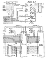
- Figs. 5a-p the partly block and partly schematic diagrams of a circuit realization of the illustrated system, signals and operating potentials are coupled to and from the system's internal bus 140, Figs. 5a-c.
- ⁇ P 40 includes an A/D port 0, Fig. 5d, which receives from bus 140 the VCT, IFB, KVCOM, PulseWidth Modulation CONTrol, BUFFered IFB, CLCOM, and BUFFered KVFB signals from the bus 140.
- These signals are applied through input circuitry including 270 ⁇ -- .0.1 ⁇ F RC circuits and back-to-back diode protection circuits to the P0.7--P0.1 terminals, respectively, of port 0.
- Display 100 is driven by a display driver 142, Fig. 5e, coupled between port 1 of ⁇ P 40 and display 100.
- the P1.0--P1.5 terminals of ⁇ P 40 are coupled to the I D0--1 D3, MODE, and Write terminals, respectively, of display driver 142.
- Display driver 142 illustratively is a type I CM7218A1 J1 display driver.
- the program executed by ⁇ P 40 is stored in an EPROM 144, Figs. 5f-g.
- a static RAM 146 provides storage for the calculations made by ⁇ P 40, as well as for data passed back and forth to and from a bus 148, Figs. 5h-i.
- EPROM 144 illustratively is a type 28F001BX EPROM.
- SRAM 146 illustratively is a type 43256 SRAM.
- the CANBUS I/O 102 includes a three-to-eight demultiplexer 150, Fig.
- Demultiplexer 150 illustratively is a type 74LS259 demultiplexer.
- the CANBUS I/O 102 also includes a serial-to-parallel/parallel-to-serial converter 154 and bus driver 156.
- the CAN+ and CAN- terminals of bus 148 are coupled to the BUS+ and BUS- terminals, respectively, of bus driver 156.
- the RX1 and RX0 terminals, respectively, of the S-P/P-S converter 154 are coupled to the REFerence and RX terminals, respectively, of the bus driver 156.
- the TX0 terminal of S-P/P-S converter 154 is coupled to the TX terminal of bus driver 156.
- S-P/P-S converter 154 illustratively is a type 82C200 S-P/P-S converter.
- the bus driver 156 illustratively is a type SI 9200 bus driver.
- the I/O functions include provisions for an RS232 interface. Consequently, the I/O also includes an RS232-to-TTL/TTL-to-RS232 interface 160, Fig. 5i.
- the TXD and RXD lines, terminals P2.0 and P2.1, respectively, of ⁇ P 40 are coupled to the T2i and R2o terminals, respectively, of interface 160.
- the T2o and R2i terminals of interface 160 are coupled to the TX232 and RX232 lines, respectively, of the bus 148.
- Interface 160 illustratively is a type MAX232 interface.
- Analog signals to the output circuit, Figs. 5 j-p, are generated by a D/A converter 164, Fig. 5g, whose input port DB0--DB7 is coupled to the P3.0-P3.7 terminals, respectively, of ⁇ P 40 via the system AD0--AD7 lines, respectively.
- the Vout A and Vout B terminals of D/A converter 164 form the KVSET and I SET lines, respectively, of the bus 148.
- D/A converter 164 illustratively is a type DAC8229 D/A converter.
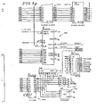
- the node address of ⁇ P 40 on the CANBUS is established by an octal switch 166, Fig.
- Octal latch 168 illustratively is a type 74ALS245 octal latch.
- the system is designed to control a number of different types of power supplies, some using high-Q, high magnitude power supply input transformers 133 as taught in U. S. Patent 5,159,544, and some using relatively lower-Q, high magnitude power supply input transformers 133.
- the system needs to be able to identify the type of power supply it is controlling.
- a line, notRP1000 identifies the power supply being controlled by the illustrated system as one having a high-Q input transformer 133 or not.
- This line of the bus 148 instructs one bit of input to ⁇ P 40 via one switch of a quad switch 171.
- Another switch of quad switch 171 is the system's manual HV On switch.
- Another quad switch 173 controls the system's initialization sequence.
- These switches are coupled via an octal latch 170 to the system AD0--AD7 lines.
- Latch 170 illustratively is a type 74ALS245 octal latch.
- the AD0-AD7 lines are also coupled to the D0-D7 terminals, respectively, of EPROM 144, the O0--O7 terminals, respectively, of SRAM 146, and the AD0-AD7 terminals, respectively, of P-S/S-P converter 154.
- the ADO-AD7 lines are also coupled to the D0-D7 lines, respectively, of a buffer/latch 174, Fig. 5f.
- the output terminals Q0--Q7 of buffer/latch 174 are coupled to the system A0-A7 lines, respectively.
- Buffer/latch 174 illustratively is a type 74ALS573 buffer/latch.
- the system A0--A7 lines are coupled to the AO-A7 terminals of EPROM 144, respectively, and to the AO-A7 terminals of SRAM 146, respectively.
- the P4.0--P4.7 terminals of ⁇ P 40 are coupled via the system A8--A15 lines, respectively, to the A8--A15 terminals, respectively, of EPROM 144, and the A8--A14 lines are also coupled to the A8--A14 terminals of SRAM 146, respectively.
- High Voltage On, High Voltage ReaDY, OVerCURrent and FeedBack FauLT status is indicated to the operator by, among other things, LEDs coupled through appropriate amplifiers to respective ones of the HS0.3, HS0.2, HS0.1, and HS0.0 terminals of ⁇ P 40.
- An EEPROM 180, Fig. 5d, containing initializing parameters for the ⁇ P 40 has its DO, DI, SK and CS terminals, respectively, coupled to the ⁇ P 40's P2.4-P2.7 terminals.
- EEPROM 180 illustratively is a type 93C46 EEPROM.
- CANBUS ACTIVE and CANBUS ERROR status is indicated by, among other things, LEDs coupled through appropriate amplifiers, Fig. 5h, to the Q6 and Q7 terminals, respectively, of demultiplexer 150.
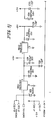
- the output circuit includes a phase locked loop IC 198, Fig. 5 l, and the A and B drive transistors 132, 134, Fig. 5 o.
- the SIG IN input to the PLL IC 198 is the PhaseLock FeedBack signal shaped by an RC circuit including a .0047 ⁇ F capacitor to ground and the series combination of a 01 ⁇ F capacitor and a 1K ⁇ resistor.
- the SIG IN input terminal of PLL IC 198 is also coupled to the not Phase Lock IN A signal line.
- PLL IC 198 illustratively is a type CD4046 PLL IC.
- Transistors 132, 134 illustratively are type IRF540 FETs.
- the drive signal for transistor 132 is output from the VOUT terminal of the PLL IC 198 to the CLocK input terminal of a D flip-flop 200.
- the oppositely phased Q and notQ outputs of D FF 200 are coupled to two push-pull configured predriver transistor pairs 202, 204, respectively, the outputs of which are coupled through respective wave-shaping parallel RC circuits 206 to the gates of the respective A and B drive transistors 132, 134.
- the drains of the respective A and B drive transistors 132, 134 are coupled to the opposite ends, the Drive A and Drive B terminals, respectively, of the primary winding 133a, Fig. 5 p, of the input transformer 133 of the high magnitude potential supply.
- D FF 200 illustratively is a type CD4013 D FF.
- Transistor pairs 202, 204 illustratively are type TPQ6002 transistor pairs.
- the remainder of the PLL circuit is generally as described in U. S. Patent 5,159,544.
- the PC I SET signal the current setting coming over to the system from the PLC, is coupled through a 100 K ⁇ input resistor to the noninverting (+) input terminal of a difference amplifier 210.
- the + input terminal of amplifier 210 is coupled through a 49.9 K ⁇ resistor to ground.
- the Analog GrouND line of the system bus is coupled through a 100 K ⁇ input resistor to the inverting (-) input terminal of amplifier 210.
- the - input terminal of amplifier 210 is coupled through a 49.9 K ⁇ feedback resistor to its output terminal.
- the output terminal of amplifier 210 is coupled through a normally closed pair 212a of relay 212 contacts to a terminal 214.
- the normally open pair 212b of contacts of relay 212 is coupled across terminal 214 and the wiper of a 1 K ⁇ potentiometer 218. This arrangement permits the operator to select either PLC control of the current setting of the system or front panel control of the current setting via potentiometer 218.
- a similar configuration including an amplifier 220 permits the system operator to select either PLC control or front panel control of the desired output high potential magnitude of the high magnitude potential supply.
- the PC KV SET signal line is coupled through a 100 K ⁇ input resistor to the + input terminal of amplifier 220.
- Analog GrouND is coupled through a 100 K ⁇ resistor to the -input terminal of amplifier 220.
- An RC parallel feedback circuit including a 25.2 K ⁇ resistor and a .01 ⁇ F capacitor is coupled across the - input terminal and the output terminal of amplifier 220.
- the output terminal of amplifier 220 is coupled through the normally closed terminals 222a of a relay 222 to the KV COMmanded line of the system bus.
- This signal is alternately selectable at the operator's option with a DC voltage established on the + input terminal of a buffer amplifier 224.
- This DC voltage is established on the wiper of a 1K ⁇ potentiometer 226.
- Potentiometer 226 is in series with an 825 ⁇ resistor and a 500 ⁇ potentiometer between + 5 VDC and ground.
- the wiper of the 500 ⁇ potentiometer is also coupled to ground so that the 825 ⁇ resistor and the setting of the 500 ⁇ potentiometer establish the minimum output high magnitude potential settable by the operator at the system front panel.
- the output of amplifier 224 is selectively coupled across the normally open terminals 222b of relay 222 to the KV COM line.
- Amplifiers 210, 220 and 224 illustratively are 3/4 of a type LF444
- the IFB signal from the system bus is coupled to the + input terminal of amplifier 114 via a 47 K ⁇ input resistor.
- a .22 ⁇ f capacitor is coupled between the + input terminal of amplifier 114 and ground.
- the output terminal of amplifier 114 is coupled to its - input terminal in buffer configuration, and forms the BUFFered IFB terminal which is coupled to the ⁇ P 40.
- the KVFB signal from the system bus is coupled to the + input terminal of amplifier 88 via a 1 K ⁇ input resistor.
- the + input terminal of amplifier 88 is clamped between + .6 VDC and - 15.6 VDC by diodes 226, 228 on its + input terminal.
- the output terminal of amplifier 88 is coupled to its - input terminal in buffer configuration, and forms the BUFFered KVFB terminal which is coupled to the ⁇ P 40.
- BUFFKVFB is also coupled to terminal 118a of PRImary/SECondary FeedBack switch 118.
- Terminal 118b of switch 118 is coupled to the - input terminal of scaling amplifier 120 via a 20 K ⁇ series resistor.
- the + input terminal of amplifier 120 is biased at +5/3 VDC by a series 20 K ⁇ --10 K ⁇ voltage divider.
- the output terminal of amplifier 120 which forms the PulseWidth Modulator CONTrol line of the system bus, is coupled through a 1 K ⁇ series resistor to the control input terminal, pin 1, of a switching regulator IC VCT regulator 86.
- VCT appears across the I+ output terminal, pin 4, of IC 86 and ground.
- VCT is fed back through series .1 ⁇ , 3 W and 21.5 K ⁇ resistors to the - input terminal of scaling amplifier 124.
- the output terminal of amplifier 124 is coupled to its - input terminal through a 15 K ⁇ feedback resistor, and to terminal 118c of switch 118.
- Amplifiers 88, 114, 120 and 124 illustratively are a type LF444CN quad amplifier.
- VCT regulator IC 86 illustratively is a type UC3524A switching regulator.
- the analog slope control circuit 116 includes a difference amplifier 230, a difference amplifier 232 and a transistor 234.
- the - input terminal of amplifier 230 receives the CurrentLimitCOMmand signal via a series 100 K ⁇ resistor from the system bus.
- a 100 K ⁇ feedback resistor is coupled between the output terminal and the - input terminal of amplifier 230.
- the output terminal of amplifier 230 is coupled through a 100 K ⁇ resistor to the - input terminal of amplifier 232.
- BUFFIFB is also coupled to the - input terminal of amplifier 232 through a 100 K ⁇ resistor.
- the - input terminal of amplifier 232 is biased negative via a 100 K ⁇ resistor to the wiper of a 100 K ⁇ potentiometer in series between - 15 VDC and ground.
- amplifier 232 is coupled through a 100 ⁇ resistor to the base of transistor 234.
- the collector of transistor 234 is coupled to ground and its emitter is coupled to the COMPensate terminal of IC 86.
- Amplifiers 230, 232 illustratively are a type LF442CN dual amplifier.
- Transistor 234 illustratively is a type 2N2907 bipolar transistor.
- the system bus Corona SSeNSe A terminal is coupled to the gate of the VCT shutdown switch 84, and to ground through a 100 KQ resistor.
- the drain of switch 84 is coupled through series 6.8 ⁇ and 390 ⁇ resistors 240, 242, respectively, to the COMP terminal of IC 86.
- a 100 ⁇ F smoothing capacitor 244 is coupled between the junction of these resistors and ground.
- the pulsewidth modulated output Corona SSeNSe A signal from ⁇ P 40 to the gate of switch 84 results in a DC voltage across capacitor 244. This voltage is summed at the COMP terminal of IC 86 with the output signal from the analog slope control circuit 116. This signal can be provided to the COMP terminal of IC 86 in other ways.
- ⁇ P 40 has a D/A output port.
- the output signal on the ⁇ P 40's D/A output port provides an even smoother signal than the Corona SSeNSe A output signal filtered by the filter 240, 242, 244 to the COMP terminal of IC 86.
- Using the pulsewidth modulated Corona SSeNSe A output signal from ⁇ P 40, filtered by filter 240, 242, 244, or the D/A port of the ⁇ P 40, permits added flexibility in applications in which more than one dispensing device 113 is coupled to the system. For example, in a single applicator 113 situation, a delay of, for example, one-half second before the achievement of full high magnitude potential can be tolerated by the system.
- IC 86 is coupled through a series 1 K ⁇ resistor and 100 pF capacitor to the common emitters of transistor pair 204.
- Switch 84 illustratively is a type IRFD210 FET.
- IC 86 and its associated components function generally as described in U. S. Patent 4,745,520.
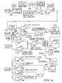
- Figs. 6-7 Flow diagrams of the routines which are executed by the ⁇ P 40 are illustrated in Figs. 6-7.
- high voltage power supply ground return current feedback, IFB, and a number of filter samples are provided to a function 342 which calculates a current feedback average, IFB AVeraGe from these variables.
- a di/dt ⁇ setting is provided to the ⁇ P 40 from a display/set functions routine 344.
- dt ⁇ and the length of a sample and hold period are provided to a decision block 346 which determines whether the change in IFB average, IFB AVG ⁇ , over the sample and hold period is greater than di/dt ⁇ .
- This decision block 346 continues to be interrogated until IFB AVG ⁇ is greater than di/dt ⁇ over the sample and hold period. Once this result is achieved, the routine next determines 348 if di/dt enable is active. This decision block 348 continues to be interrogated until di/dt enable is detected active. Once this decision 348 is achieved, di/dt is set active at 349.
- Another routine includes a decision block 350, "is High Voltage on?" This decision block 350 continues to be interrogated until HV is detected on. Once HV on is detected, a decision block 352 is reached, "is IFB greater than Current Limit COMmand?" Decision block 352 continues to be interrogated until IFB greater than CLCOM is detected. A decision block 354 is then reached, "is overcurrent enable active?" Decision block 354 continues to be interrogated until overcurrent enable is detected active. Once either di/dt or overcurrent enable is achieved, overcurrent is set active at 355.
- the ⁇ P 40 interprets 358 this occurrence as a feedback fault and disables the system. This corresponds to the situation of an input with no output.
- the ⁇ P 40 determines 360 if HV Off is active. This decision block 360 continues to be interrogated until HV Off is detected active. Once HV Off is detected active, Set HV On is disabled at 362. If HV On is not disabled along one of these paths, the ⁇ P 40 next determines 364 if the system's Interlock is active. This decision block 364 continues to be interrogated until the interlock is detected active. The interlock active decision 364 gates 365 either the "Is Programmable Logic Controller Ready Active?" decision 366 or the "Is Front Panel HV On Active?" decision 368.
- the ⁇ P 40 first determines 374 if the function Voltage Ramp is enabled. This decision block 374 continues to be interrogated until V.Ramp is enabled. Once V.Ramp is enabled, the ⁇ P 40 next determines 376 if KVFB ⁇ is greater than V.Ramp ⁇ . This decision block 376 continues to be interrogated until KVFB ⁇ is greater than V.Ramp ⁇ . Once this decision is detected, V.Ramp is set active at 378. This is one way that pulses can be furnished to the V Center Tap controller 380.
- Pulses will also be sent to VCT controller 380 if the feedback current IFB is greater than the feedback current limit, I LIMit. This decision block is illustrated at 381.
- a third way in which pulses will be sent to the VCT controller 380 is if di/dt is active. This decision is illustrated at 349. This state is detected as described above in connection with the discussion of Fig. 6. In the illustrated embodiment, this method may or may not be employed at the option 382 of the operator.
Landscapes
- Engineering & Computer Science (AREA)
- Power Engineering (AREA)
- Electrostatic Spraying Apparatus (AREA)
- Amplifiers (AREA)
- Direct Current Feeding And Distribution (AREA)
Claims (15)
- System (10) zum Aufladen eines Beschichtungsmaterials, wobei das System Folgendes aufweist:- eine Hochspannungs-Gleichspannungsquelle (12) mit einer zugehörigen Steuerung (14);- eine Beschichtungsmaterialquelle (16); und- eine Vorrichtung (18) zum Abgeben des Beschichtungsmaterials in Richtung eines mit dem Beschichtungsmaterial zu beschichtenden Gegenstandes (22), wobei die Beschichtungsmaterialabgabevorrichtung (18) an die Beschichtungsmaterialquelle (16) und an die Hochspannungs-Gleichspannungsquelle (12) angeschlossen ist, um das mittels der Beschichtungsmaterialabgabevorrichtung (18) abgegebene Beschichtungsmaterial aufzuladen,wobei die Hochspannungs-Gleichspannungsquelle (12, 14) Folgendes aufweist: einen ersten Schaltkreis (220, 224) zum Erzeugen eines ersten Signals, das zu einer gewünschten Hochspannungs-Gleichspannungsabgabe (kV) an den Hochspannungsausgangsanschlüssen der Quelle (12, 14) in Beziehung steht; einen zweiten Schaltkreis (210, 218) zum Erzeugen eines zweiten Signals, das zu einem gewünschten Ausgangsstrom in Beziehung steht, der von der Hochspannungs-Gleichspannungsquelle (12, 14) zu dem zu beschichtenden Gegenstand (22) fließt; einen dritten Schaltkreis (Q2B, Q2C, Q7) zum Zuführen der Betriebsspannung zu einem Hochspannungsvervielfacher in der Hochspannungs-Gleichspannungsquelle (12, 14), so dass der Hochspannungsvervielfacher die Hochspannungs-Gleichspannung erzeugen kann, wobei der dritte Schaltkreis (Q2B, Q2C, Q7) einen Steueranschluss aufweist; einen vierten Schaltkreis (86), der mit dem ersten und dem zweiten Schaltkreis und mit dem Steueranschluss verbunden ist, wobei der vierte Schaltkreis das erste und das zweite Signal von dem ersten (220, 224) bzw. dem zweiten (210, 218) Schaltkreis empfängt und die Betriebsspannung steuert, die dem Hochspannungsvervielfacher durch den dritten Schaltkreis (Q2B, Q2C, Q7) zugeführt wird; und einen fünften Schaltkreis (84, 240, 242, 244) zum Deaktivieren der Betriebsspannungszufuhr zu dem Hochspannungsvervielfacher, so dass durch ihn keine Hochspannungs-Gleichspannung abgegeben werden kann, wobei der fünfte Schaltkreis ebenfalls an den Steueranschluss angeschlossen ist, wobei die dem Hochspannungsvervielfacher zugeführte Betriebsspannung so gesteuert wird, dass der Ausgangsstrom, der von den Hochspannungsausgangsanschlüssen der Hochspannungs-Gleichspannungsquelle zu dem zu beschichtenden Gegenstand (22) fließt, konstant gehalten wird, wobei der vierte Schaltkreis (86) die Betriebsspannung, die dem Hochspannungsvervielfacher durch den dritten Schaltkreis (Q2B, Q2C, Q7) zugeführt wird, in Abhängigkeit von einer angewiesenen Hochspannungs-Gleichspannungseinstellung von dem ersten Schaltkreis, der angewiesenen Hochspannungs-Gleichspannungsausgangsstrom-Obergrenze von dem zweiten Schaltkreis, einem Rückkopplungssignal von dem Ausgang der Hochspannungs-Gleichspannungsquelle, einem Rückkopplungssignal des Erdrückleitungsstroms, der an der Erdrückleitungsverbindung von dem zu beschichtenden Gegenstand (22) zu der Hochspannungs-Gleichspannungsquelle fließt, und einem Rückkopplungssignal der Betriebspannung, die dem Hochspannungsvervielfacher durch den dritten Schaltkreis (Q2B, Q2C, Q7) zugeführt wird, steuert.
- System nach Anspruch 1, wobei der erste Schaltkreis (220, 224) eine programmierbare Logiksteuerung (PLC) und einen Hochgeschwindigkeitsbus zum Verbinden der PLC mit dem vierten Schaltkreis (86) aufweist.
- System nach Anspruch 1 oder 2, wobei der erste Schaltkreis (220, 224) ein erstes Potentiometer (226) zum Auswählen eines gewünschten Hochspannungs-Gleichspannungsausgangs und einen Leiter zum Verbinden des ersten Potentiometers (226) mit dem vierten Schaltkreis (86) aufweist.
- System nach Anspruch 3, das des Weiteren einen Schalter (222) zum selektiven Verbinden der PLC oder des ersten Potentiometers (226) mit dem vierten Schaltkreis (86) aufweist.
- System nach mindestens einem der vorangehenden Ansprüche, wobei der zweite Schaltkreis (210, 218) eine programmierbare Logiksteuerung (PLC) und einen Hochgeschwindigkeitsbus zum Verbinden der PLC mit dem vierten Schaltkreis (86) aufweist.
- System nach mindestens einem der vorangehenden Ansprüche, wobei der zweite Schaltkreis (210, 218) ein erstes Potentiometer (218) zum Auswählen des gewünschten Ausgangsstroms und einen Leiter zum Verbinden des ersten Potentiometers mit dem vierten Schaltkreis (86) aufweist.
- System nach Anspruch 6, das des Weiteren einen ersten Schalter (212) zum selektiven Verbinden der PLC oder des ersten Potentiometers (218) mit dem vierten Schaltkreis (86) aufweist.
- System nach mindestens einem der vorangehenden Ansprüche, wobei der zweite Schaltkreis (210, 218) ein zweites Potentiometer zum Auswählen des gewünschten Ausgangsstroms und einen Leiter zum Verbinden des zweiten Potentiometers mit dem vierten Schaltkreis (86) aufweist.
- System nach Anspruch 8, das des Weiteren einen zweiten Schalter zum selektiven Verbinden der PLC oder des zweiten Potentiometers mit dem vierten Schaltkreis (86) aufweist.
- System nach mindestens einem der vorangehenden Ansprüche, wobei der dritte Schaltkreis (Q2B, Q2C, Q7) einen Hochleistungspotenzialtransformator (133) mit einer Primärwicklung (133a) und einer Sekundärwicklung (133b) aufweist, wobei die Primärwicklung (133a) Folgendes aufweist: einen mittigen Abgriffspunkt (108) und zwei Endanschlüsse, einen ersten und einen zweiten Schalter (132, 134), die an jeweils einen der Endanschlüsse angeschlossen sind, und eine Quelle entgegengesetzt gephaster erster und zweiter Schaltsignale zum Steuern des ersten bzw. des zweiten Schalters (132, 134).
- System nach Anspruch 10, wobei der vierte Schaltkreis (86) einen Schaltregler aufweist, der einen Eingangsanschluss hat, der einen Summierungsknoten für das erste Signal und das zweite Signal bildet, und einen Ausgangsanschluss hat, der mit dem mittigen Abgriffspunkt (108) verbunden ist, wobei der fünfte Schaltkreis einen Mikroprozessor µP (40) und einen dritten Schalter (84) enthält, der mit dem µP (40) verbunden ist, um ein drittes Schaltsignal von dem µP (40) zu empfangen, wobei der dritte Schalter (84) mit dem Summierungsknoten verbunden ist, um das dritte Schaltsignal in den Schaltregler einzukoppeln, um die Zufuhr der Betriebsspannung zu dem mittigen Abgriffspunkt (108) zu deaktivieren.
- System nach Anspruch 11, wobei der dritte Schalter (84) mit dem Summierungsknoten über einen Filter (240, 242, 244) verbunden ist, der den Schaltvorgang glättet, der durch den dritten Schalter (84) in Reaktion auf die Steuerung des µP (40) veranlasst wurde.
- System nach mindestens einem der vorangehenden Ansprüche, das des Weiteren Folgendes aufweist: einen sechsten Schaltkreis, der mit dem µP (40) zusammenwirkt, um festzustellen, ob der Hochspannungs-Gleichspannungsquelle die Betriebsspannung (VCT) zugeführt wird, und einen siebenten Schaltkreis, der mit dem µP (40) zusammenwirkt, um festzustellen, ob die Hochspannungs-Gleichspannungsquelle anzeigt, dass sie eine Hochspannungs-Gleichspannung (KV) erzeugt, wobei der µP (40) eine Störung anzeigt, wenn der Hochspannungs-Gleichspannungsquelle keine Betriebsspannung (VCT) zugeführt wird und die Hochspannungs-Gleichspannungsquelle anzeigt, dass sie eine Hochspannungs-Gleichspannung (kV) erzeugt.
- System nach Anspruch 13, wobei der µP (40) eine Störung anzeigt, wenn der Hochspannungs-Gleichspannungsquelle die Betriebsspannung (VCT) zugeführt wird und die Hochspannungs-Gleichspannungsquelle anzeigt, dass sie keine Hochspannungs-Gleichspannung (HV) erzeugt.
- System nach mindestens einem der Ansprüche 1 bis 12, das des Weiteren Folgendes aufweist: einen sechsten Schaltkreis, der mit dem µP (40) zusammenwirkt, um festzustellen, ob der Hochspannungs-Gleichspannungsquelle die Betriebsspannung (VCT) zugeführt wird, und einen siebenten Schaltkreis, der mit dem µP (40) zusammenwirkt, um festzustellen, ob die Hochspannungs-Gleichspannungsquelle anzeigt, dass sie eine Hochspannungs-Gleichspannung erzeugt, wobei der µP (40) eine Störung anzeigt, wenn der Hochspannungs-Gleichspannungsquelle die Betriebsspannung (VCT) zugeführt wird und die Hochspannungs-Gleichspannungsquelle anzeigt, dass sie keine Hochspannungs-Gleichspannung (HV) erzeugt.
Applications Claiming Priority (2)
| Application Number | Priority Date | Filing Date | Title |
|---|---|---|---|
| US10258498P | 1998-09-30 | 1998-09-30 | |
| US102584P | 1998-09-30 |
Publications (3)
| Publication Number | Publication Date |
|---|---|
| EP0991173A2 EP0991173A2 (de) | 2000-04-05 |
| EP0991173A3 EP0991173A3 (de) | 2003-05-28 |
| EP0991173B1 true EP0991173B1 (de) | 2006-08-16 |
Family
ID=22290596
Family Applications (1)
| Application Number | Title | Priority Date | Filing Date |
|---|---|---|---|
| EP99116569A Revoked EP0991173B1 (de) | 1998-09-30 | 1999-08-24 | Hochspannungsversorgung |
Country Status (3)
| Country | Link |
|---|---|
| EP (1) | EP0991173B1 (de) |
| CA (1) | CA2283974C (de) |
| DE (1) | DE69932781T2 (de) |
Cited By (1)
| Publication number | Priority date | Publication date | Assignee | Title |
|---|---|---|---|---|
| EP2332658B1 (de) | 2009-12-07 | 2015-07-08 | Dürr Systems GmbH | Hochspannungssteuerung mit verbesserter Überwachung und Diagnostik |
Citations (2)
| Publication number | Priority date | Publication date | Assignee | Title |
|---|---|---|---|---|
| US3840797A (en) * | 1970-12-28 | 1974-10-08 | Us Navy | Related power supply |
| US5029062A (en) * | 1989-04-14 | 1991-07-02 | Alcatel Espace | Electrical regulation and energy transfer circuit |
Family Cites Families (13)
| Publication number | Priority date | Publication date | Assignee | Title |
|---|---|---|---|---|
| US3851618A (en) | 1974-01-14 | 1974-12-03 | Ransburg Corp | Electrostatic coating apparatus |
| US3875892A (en) | 1974-01-14 | 1975-04-08 | Ransburg Corp | Apparatus for avoiding sparks in an electrostatic coating system |
| US3894272A (en) | 1974-01-14 | 1975-07-08 | Ransburg Corp | Method and apparatus for determining incipient grounding of a high voltage electrostatic system |
| US4075677A (en) | 1976-08-09 | 1978-02-21 | Ransburg Corporation | Electrostatic coating system |
| US4187527A (en) | 1976-08-09 | 1980-02-05 | Ransburg Corporation | Electrostatic coating system |
| US4324812A (en) | 1980-05-29 | 1982-04-13 | Ransburg Corporation | Method for controlling the flow of coating material |
| US4485427A (en) | 1982-04-19 | 1984-11-27 | Ransburg Corporation | Fold-back power supply |
| US4481557A (en) | 1982-09-27 | 1984-11-06 | Ransburg Corporation | Electrostatic coating system |
| US4745520A (en) | 1986-10-10 | 1988-05-17 | Ransburg Corporation | Power supply |
| CA1316980C (en) | 1988-12-27 | 1993-04-27 | Daniel C. Hughey | Power supply |
| US5231564A (en) * | 1992-03-30 | 1993-07-27 | Lorad Corporation | Power supply for producing excitation voltage for an x-ray tube filament |
| JP3092049B2 (ja) * | 1995-09-27 | 2000-09-25 | 本田技研工業株式会社 | 静電塗装用高電圧発生装置 |
| GB2320342A (en) * | 1996-12-14 | 1998-06-17 | Jonathan Hugh Lambert Copus | Voltage supply circuit with stabilised output control |
-
1999
- 1999-08-24 DE DE69932781T patent/DE69932781T2/de not_active Revoked
- 1999-08-24 EP EP99116569A patent/EP0991173B1/de not_active Revoked
- 1999-09-27 CA CA 2283974 patent/CA2283974C/en not_active Expired - Fee Related
Patent Citations (2)
| Publication number | Priority date | Publication date | Assignee | Title |
|---|---|---|---|---|
| US3840797A (en) * | 1970-12-28 | 1974-10-08 | Us Navy | Related power supply |
| US5029062A (en) * | 1989-04-14 | 1991-07-02 | Alcatel Espace | Electrical regulation and energy transfer circuit |
Non-Patent Citations (1)
| Title |
|---|
| ZHOU D. ET AL: "A three-switch high-voltage converter", APPLIED POWER ELECTRONICS CONFERENCE AND EXPOSITION, 1995. APEC '95. CONFERENCE PROCEEDINGS 1995, 5 March 1995 (1995-03-05) - 9 March 1995 (1995-03-09), Dallas (TEXAS), USA 5-9 March 1995, pages 283 - 289, XP000528144, DOI: doi:10.1109/APEC.1995.468963 * |
Cited By (1)
| Publication number | Priority date | Publication date | Assignee | Title |
|---|---|---|---|---|
| EP2332658B1 (de) | 2009-12-07 | 2015-07-08 | Dürr Systems GmbH | Hochspannungssteuerung mit verbesserter Überwachung und Diagnostik |
Also Published As
| Publication number | Publication date |
|---|---|
| CA2283974C (en) | 2003-08-05 |
| DE69932781T2 (de) | 2007-08-23 |
| EP0991173A3 (de) | 2003-05-28 |
| DE69932781D1 (de) | 2006-09-28 |
| CA2283974A1 (en) | 2000-03-30 |
| EP0991173A2 (de) | 2000-04-05 |
Similar Documents
| Publication | Publication Date | Title |
|---|---|---|
| US6144570A (en) | Control system for a HVDC power supply | |
| US5978244A (en) | Programmable logic control system for a HVDC power supply | |
| EP0789625B1 (de) | Vorrichtung und verfahren zur beschichtung von substraten mit durch induktion geladenen harzpulverpartikeln | |
| US4324812A (en) | Method for controlling the flow of coating material | |
| EP0789632B1 (de) | Verfahren zum verbessern der elektrostatischen ladung auf pulvern | |
| CA1204818A (en) | Fold-back power supply | |
| US3794243A (en) | Electrostatic spray apparatus and method | |
| KR20040017224A (ko) | 마찰정전기적으로 하전된 유동층으로 분말 코팅하는 방법 | |
| EP0991173B1 (de) | Hochspannungsversorgung | |
| EP1028814A1 (de) | Vorrichtung zum steuern der stromversorgung einer spritzpistole | |
| US20050063131A1 (en) | Controller for electrostatic spray gun internal power supply | |
| JP2001025688A (ja) | 吹付塗装装置 | |
| EP1000666A2 (de) | Vorrichtung und Methode zur unabhängigen Steuerung von mehreren Auftragsvorrichtungen | |
| US4027050A (en) | Method and apparatus for electrostatic coating | |
| JPH02298374A (ja) | 静電塗装装置 | |
| CA2201878C (en) | Process for imparting an electrostatic charge to powders to render them useful for coating applications | |
| Knobbe | Tribo or Corona? Here's How to Decide | |
| JPS5920362Y2 (ja) | クリヤ塗装装置 | |
| Keown | Electrostatic Application Equipment for Powder Coatings | |
| HU185730B (en) | Electrostatic apparatus for spraying dusty or liquid colours | |
| Penick | Voltage Block Systems: Technological Advancements for Waterborne Electrostatic Painting | |
| IL117020A (en) | Process for imparting an electrostatic charge to powders and rendering them useful for coating applications | |
| MXPA99010252A (en) | Method and device for independently controlling material multiple applicators |
Legal Events
| Date | Code | Title | Description |
|---|---|---|---|
| PUAI | Public reference made under article 153(3) epc to a published international application that has entered the european phase |
Free format text: ORIGINAL CODE: 0009012 |
|
| AK | Designated contracting states |
Kind code of ref document: A2 Designated state(s): AT BE CH CY DE DK ES FI FR GB GR IE IT LI LU MC NL PT SE |
|
| AX | Request for extension of the european patent |
Free format text: AL;LT;LV;MK;RO;SI |
|
| 17P | Request for examination filed |
Effective date: 20000822 |
|
| PUAL | Search report despatched |
Free format text: ORIGINAL CODE: 0009013 |
|
| AK | Designated contracting states |
Designated state(s): AT BE CH CY DE DK ES FI FR GB GR IE IT LI LU MC NL PT SE |
|
| AX | Request for extension of the european patent |
Extension state: AL LT LV MK RO SI |
|
| RIC1 | Information provided on ipc code assigned before grant |
Ipc: 7H 02M 3/07 B Ipc: 7B 05B 5/10 B Ipc: 7H 02M 7/10 A |
|
| AKX | Designation fees paid |
Designated state(s): CH DE IT LI |
|
| 17Q | First examination report despatched |
Effective date: 20040419 |
|
| GRAP | Despatch of communication of intention to grant a patent |
Free format text: ORIGINAL CODE: EPIDOSNIGR1 |
|
| GRAS | Grant fee paid |
Free format text: ORIGINAL CODE: EPIDOSNIGR3 |
|
| GRAA | (expected) grant |
Free format text: ORIGINAL CODE: 0009210 |
|
| AK | Designated contracting states |
Kind code of ref document: B1 Designated state(s): CH DE IT LI |
|
| PG25 | Lapsed in a contracting state [announced via postgrant information from national office to epo] |
Ref country code: LI Free format text: LAPSE BECAUSE OF FAILURE TO SUBMIT A TRANSLATION OF THE DESCRIPTION OR TO PAY THE FEE WITHIN THE PRESCRIBED TIME-LIMIT Effective date: 20060816 Ref country code: CH Free format text: LAPSE BECAUSE OF FAILURE TO SUBMIT A TRANSLATION OF THE DESCRIPTION OR TO PAY THE FEE WITHIN THE PRESCRIBED TIME-LIMIT Effective date: 20060816 |
|
| REG | Reference to a national code |
Ref country code: CH Ref legal event code: EP |
|
| REF | Corresponds to: |
Ref document number: 69932781 Country of ref document: DE Date of ref document: 20060928 Kind code of ref document: P |
|
| REG | Reference to a national code |
Ref country code: CH Ref legal event code: PL |
|
| PLBI | Opposition filed |
Free format text: ORIGINAL CODE: 0009260 |
|
| 26 | Opposition filed |
Opponent name: VISHAY ELECTRONIC GMBH Effective date: 20070515 |
|
| PLAX | Notice of opposition and request to file observation + time limit sent |
Free format text: ORIGINAL CODE: EPIDOSNOBS2 |
|
| PLBB | Reply of patent proprietor to notice(s) of opposition received |
Free format text: ORIGINAL CODE: EPIDOSNOBS3 |
|
| PGFP | Annual fee paid to national office [announced via postgrant information from national office to epo] |
Ref country code: IT Payment date: 20080826 Year of fee payment: 10 |
|
| PGFP | Annual fee paid to national office [announced via postgrant information from national office to epo] |
Ref country code: DE Payment date: 20080930 Year of fee payment: 10 |
|
| RDAF | Communication despatched that patent is revoked |
Free format text: ORIGINAL CODE: EPIDOSNREV1 |
|
| RDAG | Patent revoked |
Free format text: ORIGINAL CODE: 0009271 |
|
| STAA | Information on the status of an ep patent application or granted ep patent |
Free format text: STATUS: PATENT REVOKED |
|
| 27W | Patent revoked |
Effective date: 20090528 |