EP0991309A1 - Procede de reduction des ondes electromagnetiques emises par un dispositif electronique - Google Patents
Procede de reduction des ondes electromagnetiques emises par un dispositif electronique Download PDFInfo
- Publication number
- EP0991309A1 EP0991309A1 EP97922086A EP97922086A EP0991309A1 EP 0991309 A1 EP0991309 A1 EP 0991309A1 EP 97922086 A EP97922086 A EP 97922086A EP 97922086 A EP97922086 A EP 97922086A EP 0991309 A1 EP0991309 A1 EP 0991309A1
- Authority
- EP
- European Patent Office
- Prior art keywords
- electronic device
- electromagnetic radiation
- cables
- electrically conductive
- cabinet
- Prior art date
- Legal status (The legal status is an assumption and is not a legal conclusion. Google has not performed a legal analysis and makes no representation as to the accuracy of the status listed.)
- Granted
Links
Images


Classifications
-
- H—ELECTRICITY
- H05—ELECTRIC TECHNIQUES NOT OTHERWISE PROVIDED FOR
- H05K—PRINTED CIRCUITS; CASINGS OR CONSTRUCTIONAL DETAILS OF ELECTRIC APPARATUS; MANUFACTURE OF ASSEMBLAGES OF ELECTRICAL COMPONENTS
- H05K9/00—Screening of apparatus or components against electric or magnetic fields
- H05K9/0007—Casings
- H05K9/0018—Casings with provisions to reduce aperture leakages in walls, e.g. terminals, connectors, cables
-
- Y—GENERAL TAGGING OF NEW TECHNOLOGICAL DEVELOPMENTS; GENERAL TAGGING OF CROSS-SECTIONAL TECHNOLOGIES SPANNING OVER SEVERAL SECTIONS OF THE IPC; TECHNICAL SUBJECTS COVERED BY FORMER USPC CROSS-REFERENCE ART COLLECTIONS [XRACs] AND DIGESTS
- Y10—TECHNICAL SUBJECTS COVERED BY FORMER USPC
- Y10T—TECHNICAL SUBJECTS COVERED BY FORMER US CLASSIFICATION
- Y10T29/00—Metal working
- Y10T29/49—Method of mechanical manufacture
- Y10T29/49002—Electrical device making
- Y10T29/49117—Conductor or circuit manufacturing
-
- Y—GENERAL TAGGING OF NEW TECHNOLOGICAL DEVELOPMENTS; GENERAL TAGGING OF CROSS-SECTIONAL TECHNOLOGIES SPANNING OVER SEVERAL SECTIONS OF THE IPC; TECHNICAL SUBJECTS COVERED BY FORMER USPC CROSS-REFERENCE ART COLLECTIONS [XRACs] AND DIGESTS
- Y10—TECHNICAL SUBJECTS COVERED BY FORMER USPC
- Y10T—TECHNICAL SUBJECTS COVERED BY FORMER US CLASSIFICATION
- Y10T29/00—Metal working
- Y10T29/49—Method of mechanical manufacture
- Y10T29/49002—Electrical device making
- Y10T29/49117—Conductor or circuit manufacturing
- Y10T29/49123—Co-axial cable
-
- Y—GENERAL TAGGING OF NEW TECHNOLOGICAL DEVELOPMENTS; GENERAL TAGGING OF CROSS-SECTIONAL TECHNOLOGIES SPANNING OVER SEVERAL SECTIONS OF THE IPC; TECHNICAL SUBJECTS COVERED BY FORMER USPC CROSS-REFERENCE ART COLLECTIONS [XRACs] AND DIGESTS
- Y10—TECHNICAL SUBJECTS COVERED BY FORMER USPC
- Y10T—TECHNICAL SUBJECTS COVERED BY FORMER US CLASSIFICATION
- Y10T29/00—Metal working
- Y10T29/49—Method of mechanical manufacture
- Y10T29/49002—Electrical device making
- Y10T29/49117—Conductor or circuit manufacturing
- Y10T29/49169—Assembling electrical component directly to terminal or elongated conductor
Definitions
- the present invention relates to a method of reducing electromagnetic radiation from an electronic device.
- FIG. 4 is a schematic perspective view of the conventional electronic device and its connected state.
- the electronic device has an electronic device unit 41 having a cabinet 41a and a cable connection opening 42, a peripheral 43 having a cabinet 43a, and cables 44.
- the electronic device is composed of the electronic device unit 41 and the peripheral 43 which are interconnected by the cables 44.
- the cables 44 are connected to terminals of the electronic device unit 41 through the opening 42 defined in a lower portion of the cabinet 41a.
- the electronic device unit 41, the peripheral 43, and the cables 44 are shielded to prevent electromagnetic radiation generated from internal units of the electronic device unit 41 and the peripheral 43 from affecting the surroundings of the system.
- a method of reducing electromagnetic radiation emitted outwardly from an electronic device including an electronic device unit, a peripheral thereof, and a plurality of cables electrically interconnecting the electronic device unit and the peripheral.
- a cabinet of the electronic device unit, a cabinet of the peripheral, and the cables are shielded, and a soft cloth-like electromagnetic radiation shield is placed in a covering relation to an opening defined in the cabinet to allow the cables to be connected to terminals of the electronic device unit.
- the electromagnetic radiation shield is attached in an electrically conductive fashion to the cabinet so as to be openable and closable with respect to the opening.
- the cloth-like electromagnetic radiation shield preferably has a plurality of vertical slits defined therein for passage of the cables therethrough, with a lower side of the electromagnetic radiation shield being a free end.
- a plurality of the cloth-like electromagnetic radiation shields may be superposed and attached.
- the free end of the cloth-like electromagnetic radiation shield, which is divided by the slits, may have a vertical length long enough to wrap the cables near portions thereof which pass through the slits.
- the cloth-like electromagnetic radiation shield may be made of electrically conductive fibers, or electrically conductive resin, or electrically conductive rubber.
- the cables may be passed through the opening at any spot without removal of the electromagnetic radiation shield.
- the electromagnetic radiation shield may have vertical slits, may be provided as plural electromagnetic radiation shields, and may have its skirt elongated to wrap the cables for reducing open cracks between the electromagnetic radiation shield and the cables for an increased shielding capability. Therefore, because the electromagnetic radiation shield means can increase the electromagnetic radiation shielding capability regardless of the number of the cables, the electromagnetic radiation shield means may be constructed as a general-purpose product, and may be attached and removed with ease.
- the cabinet of the electronic device unit, the cabinet of the peripheral, and the cables are shielded, and an electrically conductive material which is plastic at normal temperature is filled in the form of a sheet in open cracks between the cables inserted in an opening defined in the cabinet to allow the cables to be connected to terminals of the electronic device and the cabinet surrounding the opening.
- the electrically conductive material which is plastic at normal temperature, such as resin, in the form of a sheet
- electromagnetic radiation emitted from within the cabinet through the opening is reduced regardless of the number of the cables. Since the filled material is plastic at normal temperature, it can easily be removed and filled again when the cables are removed and installed.
- the method of reducing electromagnetic radiation can also effectively be applied to a semiconductor testing device.
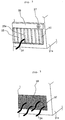
- Fig. 1A is a schematic perspective view showing an electronic device unit, a peripheral, and a connected state therebetween, of an electronic device according to a first embodiment of the present invention
- Fig. 1B is an enlarged fragmentary perspective view of an opening in the electronic device unit according to the first embodiment of the present invention.
- the electronic device has an electronic device unit 11 having a cabinet 11a which has an opening 12, a peripheral 13 having a cabinet 13a, cables 14, an electrically conductive cloth 15 having slits 15a, a shield plate 16, and mounting screws 17.
- the electronic device is composed of the electronic device unit 11 and the peripheral 13 which are interconnected by the cables 14.
- the cables 14 are connected to terminals of the electronic device unit 11 through the opening 12 defined in a lower portion of the cabinet 11a and having an electromagnetic radiation shield means for the cabinet 11a.
- the electronic device unit 11, the peripheral 13, and the cables 14 are shielded by a technology that has already been practiced, for preventing electromagnetic radiation generated from internal units of the electronic device unit 11 affecting surroundings of the system.
- the electromagnetic radiation shield means comprises an electrically conductive cloth 15 made of electrically conductive fibers such as carbon fibers or the like and having a number of slits 15a, an electrically conductive shield plate 16 pressing the electrically conductive cloth 15 against the cabinet 11a which is electrically conductive, and mounting screws 17 by which the shield plate 16 is fastened to the cabinet 11a.
- the electrically conductive cloth 15 has a size large enough to fully cover the opening 12, and is clamped by the shield plate 16 pressed against the cabinet 11a by the mounting screws 17 and fixed in an electrically conductive fashion to the cabinet 11a which is electrically conductive.
- the cables 14 extend through the slits 15a in the electrically conductive cloth 15, and are connected to the terminals of the electronic device unit 11. Since the electrically conductive cloth 15 is a piece of fabric having the slits 15a, it allows the cables 14 to pass therethrough at any spot. The electrically conductive cloth 15 covers almost all the opening 12, it can block electromagnetic radiation substantially in its entirety which is emitted from within the electronic device unit 11.
- Fig. 2 is an enlarged fragmentary perspective view of an opening in an electronic device unit according to a second embodiment of the present invention.
- the electronic device has a cabinet 21a has an opening 22, cables 24, electrically conductive cloths 25 having slits 25a, a shield plate 26, and mounting screws 27.
- the plural electrically conductive cloths 25 can reduce open cracks produced by passing the cables 26 therethrough for thereby improving a shielding capability.
- the slits 25a in the electrically conductive cloths 25 are aligned with each other. However, the slits 25a in the electrically conductive cloths 25 may be in different positions.
- the electrically conductive cloth with the slits according to the first and second embodiments shown in Figs. 1A, 1B, and 2 has a skirt section elongated to wrap the cables passing through the slits for thereby reducing open cracks between the electrically conductive cloth and the cables to further reduce the outward emission of electromagnetic radiation from within the cabinet.
- the electromagnetic radiation shield means employs the electrically conductive cloth or cloths.
- the electromagnetic radiation shield means may comprise electromagnetic radiation resin or rubber which is soft at normal temperature. While the skirt has been described with respect to the above embodiments in which the electrically conductive cloth has slits, the skirt elongated to wrap the cables passing therethrough is effective to reduce the outward emission of electromagnetic radiation from within the cabinet even if the electrically conductive cloth has no slits.
- Fig. 3 is an enlarged fragmentary perspective view of an opening in an electronic device unit according to a fourth embodiment of the present invention.
- the electronic device has a cabinet 31a has an opening 32, cables 34, and electrically conductive resin 38 which is plastic at normal temperature.
- the electromagnetic radiation shield means comprises electromagnetic radiation resin 38 which is plastic at normal temperature, filled in the space of the opening 32 through which the cables 34 extend.
- the electromagnetic radiation resin 38 which is sticky and plastic at normal temperature is filled in the form of a sheet in the space of the opening 32 through which the cables 34 extend, for thereby reducing electromagnetic radiation emitted from within the cabinet 31a through the opening 32. Since the filled material is plastic at normal temperature, it can easily be removed and filled again when the cables 34 are removed and installed.
- the filled material may be rubber or fiber rather than resin insofar as it is electrically conductive and plastic at normal temperature.
Landscapes
- Engineering & Computer Science (AREA)
- Microelectronics & Electronic Packaging (AREA)
- Shielding Devices Or Components To Electric Or Magnetic Fields (AREA)
- Apparatuses And Processes For Manufacturing Resistors (AREA)
- Grinding-Machine Dressing And Accessory Apparatuses (AREA)
- Dc Machiner (AREA)
- Dynamo-Electric Clutches, Dynamo-Electric Brakes (AREA)
- Details Of Measuring And Other Instruments (AREA)
Applications Claiming Priority (5)
| Application Number | Priority Date | Filing Date | Title |
|---|---|---|---|
| JP14934496 | 1996-06-11 | ||
| JP14934496 | 1996-06-11 | ||
| JP9101873A JPH1065381A (ja) | 1996-06-11 | 1997-04-18 | 電子機器の放射電磁波低減方法 |
| JP10187397 | 1997-04-18 | ||
| PCT/JP1997/001665 WO1997048262A1 (fr) | 1996-06-11 | 1997-05-19 | Procede de reduction des ondes electromagnetiques emises par un dispositif electronique |
Publications (3)
| Publication Number | Publication Date |
|---|---|
| EP0991309A1 true EP0991309A1 (fr) | 2000-04-05 |
| EP0991309A4 EP0991309A4 (fr) | 2000-04-05 |
| EP0991309B1 EP0991309B1 (fr) | 2004-08-25 |
Family
ID=26442648
Family Applications (1)
| Application Number | Title | Priority Date | Filing Date |
|---|---|---|---|
| EP97922086A Expired - Lifetime EP0991309B1 (fr) | 1996-06-11 | 1997-05-19 | Procede de reduction des ondes electromagnetiques emises par un dispositif electronique |
Country Status (6)
| Country | Link |
|---|---|
| US (1) | US6101711A (fr) |
| EP (1) | EP0991309B1 (fr) |
| JP (1) | JPH1065381A (fr) |
| AT (1) | ATE274789T1 (fr) |
| DE (1) | DE69730448T2 (fr) |
| WO (1) | WO1997048262A1 (fr) |
Cited By (3)
| Publication number | Priority date | Publication date | Assignee | Title |
|---|---|---|---|---|
| GB2479351A (en) * | 2010-04-06 | 2011-10-12 | Nanotesla Inst Ljubljana | Magnetically lossy cover for apertures through an electromagnetic shielding wall |
| GB2485780A (en) * | 2010-11-23 | 2012-05-30 | Cp Cases Ltd | Port for cable entry into chassis providing EMI suppression and comprising a compressible conducting seal with a slit |
| EP3139719A1 (fr) * | 2015-09-07 | 2017-03-08 | Lapp Engineering & Co. | Dispositif de mise en contact pour passe-cables et passe-cable |
Families Citing this family (6)
| Publication number | Priority date | Publication date | Assignee | Title |
|---|---|---|---|---|
| US6713672B1 (en) * | 2001-12-07 | 2004-03-30 | Laird Technologies, Inc. | Compliant shaped EMI shield |
| US9055665B2 (en) * | 2010-11-18 | 2015-06-09 | Nagravision S.A.S | Interface between a security module and a host device |
| CA2835601C (fr) * | 2011-05-11 | 2019-09-10 | Stemrad Ltd. | Dispositif de radioprotection et procedes de celui-ci |
| EP3270722B1 (fr) | 2015-03-17 | 2020-10-21 | StemRad Ltd. | Dispositif de protection contre les rayonnements dans l'espace |
| JP6611505B2 (ja) * | 2015-07-30 | 2019-11-27 | キヤノン株式会社 | 電気機器、及び導電性部材の配置方法 |
| EP3438005B1 (fr) | 2017-08-02 | 2023-05-31 | StemRad Ltd. | Configuration de matériau facilitant la flexibilité d'une structure à l'aide de composants rigides |
Family Cites Families (10)
| Publication number | Priority date | Publication date | Assignee | Title |
|---|---|---|---|---|
| US4308417A (en) * | 1979-06-19 | 1981-12-29 | International Computers Limited | Electrical sealing device |
| JPS57132499U (fr) * | 1981-02-10 | 1982-08-18 | ||
| IE851076L (en) * | 1985-04-29 | 1986-10-29 | Prendergast Patrick Thomas | Shield for electronic apparatus |
| JPH0235495U (fr) * | 1988-08-30 | 1990-03-07 | ||
| JPH033781U (fr) * | 1989-06-02 | 1991-01-16 | ||
| JPH0361391U (fr) * | 1989-10-20 | 1991-06-17 | ||
| JP2833107B2 (ja) * | 1990-02-23 | 1998-12-09 | 日本電気株式会社 | 電磁遮へい体 |
| SE466182B (sv) * | 1990-05-15 | 1992-01-07 | Norsk Data Ab | Saekerhetsanordning vid datorutrustningar |
| JPH04259516A (ja) * | 1991-02-13 | 1992-09-16 | Hitachi Kasei Mold Kk | プラスチック成形品の製造法 |
| JPH08236968A (ja) * | 1995-02-22 | 1996-09-13 | Nippon Telegr & Teleph Corp <Ntt> | プリント板前面パネル |
-
1997
- 1997-04-18 JP JP9101873A patent/JPH1065381A/ja active Pending
- 1997-05-19 US US09/147,365 patent/US6101711A/en not_active Expired - Lifetime
- 1997-05-19 EP EP97922086A patent/EP0991309B1/fr not_active Expired - Lifetime
- 1997-05-19 DE DE69730448T patent/DE69730448T2/de not_active Expired - Lifetime
- 1997-05-19 AT AT97922086T patent/ATE274789T1/de not_active IP Right Cessation
- 1997-05-19 WO PCT/JP1997/001665 patent/WO1997048262A1/fr not_active Ceased
Cited By (7)
| Publication number | Priority date | Publication date | Assignee | Title |
|---|---|---|---|---|
| GB2479351A (en) * | 2010-04-06 | 2011-10-12 | Nanotesla Inst Ljubljana | Magnetically lossy cover for apertures through an electromagnetic shielding wall |
| GB2479351B (en) * | 2010-04-06 | 2012-07-18 | Nanotesla Inst Ljubljana | Lossy cover for apertures through a shielding wall |
| GB2485780A (en) * | 2010-11-23 | 2012-05-30 | Cp Cases Ltd | Port for cable entry into chassis providing EMI suppression and comprising a compressible conducting seal with a slit |
| WO2012069829A1 (fr) * | 2010-11-23 | 2012-05-31 | Cp Cases Ltd | Accès destiné à éviter le rayonnement électromagnétique |
| GB2485780B (en) * | 2010-11-23 | 2014-10-08 | Cp Cases Ltd | Port |
| US8969738B2 (en) | 2010-11-23 | 2015-03-03 | Cp Cases Ltd | Port for inhibiting electromagnetic radiation |
| EP3139719A1 (fr) * | 2015-09-07 | 2017-03-08 | Lapp Engineering & Co. | Dispositif de mise en contact pour passe-cables et passe-cable |
Also Published As
| Publication number | Publication date |
|---|---|
| JPH1065381A (ja) | 1998-03-06 |
| US6101711A (en) | 2000-08-15 |
| ATE274789T1 (de) | 2004-09-15 |
| EP0991309B1 (fr) | 2004-08-25 |
| EP0991309A4 (fr) | 2000-04-05 |
| DE69730448D1 (de) | 2004-09-30 |
| WO1997048262A1 (fr) | 1997-12-18 |
| DE69730448T2 (de) | 2005-09-08 |
Similar Documents
| Publication | Publication Date | Title |
|---|---|---|
| US4785136A (en) | Electromagnetic interference shielding cover | |
| US6101711A (en) | Method for reducing electromagnetic waves radiated from electronic device | |
| EP0843512A3 (fr) | Blindage électromagnétique haute fréquence avec aération pour l'enveloppe d'un dispositif électronique | |
| JPS63216553A (ja) | Mri用rfセルフシ−ルド | |
| US20030037942A1 (en) | EMI enclosure having a flexible cable shield | |
| US6140575A (en) | Shielded electronic circuit assembly | |
| US6243274B1 (en) | Shields for electronic components with ready access to shielded components | |
| US4498715A (en) | Cable shield grounding clamp | |
| FR2716580B1 (fr) | Boîte de raccordement pour une pluralité de câbles blindés. | |
| EP1150555A2 (fr) | Boítier pour convertisseur de fréquence | |
| KR970071967A (ko) | 영상표시기기의 편향요크 누설전계 차폐장치 | |
| RU96122531A (ru) | Видеодисплей, включающий устройство экранирования электромагнитного поля, образуемого отклоняющей системой | |
| CA2015756A1 (fr) | Connecteur electrique blinde | |
| JPH0651026Y2 (ja) | 電子機器筐体のシールド構造 | |
| JPH10294587A (ja) | 電磁波ノイズ対策装置 | |
| CN209783609U (zh) | 磁编码器的隔磁装置 | |
| US6375361B1 (en) | Optical fiber connector electromagnetic shield assembly | |
| JPH088578A (ja) | 簡易シールドルーム | |
| JP2879055B2 (ja) | シールドケース | |
| JPS63313899A (ja) | Icのシ−ルド装置 | |
| CN215188122U (zh) | 一种具有电磁波屏蔽功能的玻璃制备装置 | |
| JPH066558Y2 (ja) | テレビ共聴用機器 | |
| JPH07162188A (ja) | 電磁シールド装置 | |
| JPH113796A (ja) | 雷サージ誘導による無線設備破損防止方法及び装置 | |
| JPH0516331U (ja) | 電子機器の輻射ノイズ防止機構 |
Legal Events
| Date | Code | Title | Description |
|---|---|---|---|
| PUAI | Public reference made under article 153(3) epc to a published international application that has entered the european phase |
Free format text: ORIGINAL CODE: 0009012 |
|
| 17P | Request for examination filed |
Effective date: 19981217 |
|
| A4 | Supplementary search report drawn up and despatched |
Effective date: 19990723 |
|
| AK | Designated contracting states |
Kind code of ref document: A4 Designated state(s): AT DE ES FR GB IE IT NL PT Kind code of ref document: A1 Designated state(s): AT DE ES FR GB IE IT NL PT |
|
| 17Q | First examination report despatched |
Effective date: 20021218 |
|
| GRAP | Despatch of communication of intention to grant a patent |
Free format text: ORIGINAL CODE: EPIDOSNIGR1 |
|
| GRAS | Grant fee paid |
Free format text: ORIGINAL CODE: EPIDOSNIGR3 |
|
| GRAA | (expected) grant |
Free format text: ORIGINAL CODE: 0009210 |
|
| AK | Designated contracting states |
Kind code of ref document: B1 Designated state(s): AT DE ES FR GB IE IT NL PT |
|
| PG25 | Lapsed in a contracting state [announced via postgrant information from national office to epo] |
Ref country code: NL Free format text: LAPSE BECAUSE OF FAILURE TO SUBMIT A TRANSLATION OF THE DESCRIPTION OR TO PAY THE FEE WITHIN THE PRESCRIBED TIME-LIMIT Effective date: 20040825 Ref country code: IT Free format text: LAPSE BECAUSE OF FAILURE TO SUBMIT A TRANSLATION OF THE DESCRIPTION OR TO PAY THE FEE WITHIN THE PRESCRIBED TIME-LIMIT;WARNING: LAPSES OF ITALIAN PATENTS WITH EFFECTIVE DATE BEFORE 2007 MAY HAVE OCCURRED AT ANY TIME BEFORE 2007. THE CORRECT EFFECTIVE DATE MAY BE DIFFERENT FROM THE ONE RECORDED. Effective date: 20040825 Ref country code: FR Free format text: LAPSE BECAUSE OF FAILURE TO SUBMIT A TRANSLATION OF THE DESCRIPTION OR TO PAY THE FEE WITHIN THE PRESCRIBED TIME-LIMIT Effective date: 20040825 Ref country code: AT Free format text: LAPSE BECAUSE OF FAILURE TO SUBMIT A TRANSLATION OF THE DESCRIPTION OR TO PAY THE FEE WITHIN THE PRESCRIBED TIME-LIMIT Effective date: 20040825 |
|
| REG | Reference to a national code |
Ref country code: GB Ref legal event code: FG4D |
|
| REG | Reference to a national code |
Ref country code: IE Ref legal event code: FG4D |
|
| REF | Corresponds to: |
Ref document number: 69730448 Country of ref document: DE Date of ref document: 20040930 Kind code of ref document: P |
|
| PG25 | Lapsed in a contracting state [announced via postgrant information from national office to epo] |
Ref country code: ES Free format text: LAPSE BECAUSE OF FAILURE TO SUBMIT A TRANSLATION OF THE DESCRIPTION OR TO PAY THE FEE WITHIN THE PRESCRIBED TIME-LIMIT Effective date: 20041206 |
|
| NLV1 | Nl: lapsed or annulled due to failure to fulfill the requirements of art. 29p and 29m of the patents act | ||
| PG25 | Lapsed in a contracting state [announced via postgrant information from national office to epo] |
Ref country code: IE Free format text: LAPSE BECAUSE OF NON-PAYMENT OF DUE FEES Effective date: 20050519 Ref country code: GB Free format text: LAPSE BECAUSE OF NON-PAYMENT OF DUE FEES Effective date: 20050519 |
|
| PLBE | No opposition filed within time limit |
Free format text: ORIGINAL CODE: 0009261 |
|
| STAA | Information on the status of an ep patent application or granted ep patent |
Free format text: STATUS: NO OPPOSITION FILED WITHIN TIME LIMIT |
|
| 26N | No opposition filed |
Effective date: 20050526 |
|
| EN | Fr: translation not filed | ||
| GBPC | Gb: european patent ceased through non-payment of renewal fee |
Effective date: 20050519 |
|
| REG | Reference to a national code |
Ref country code: IE Ref legal event code: MM4A |
|
| PG25 | Lapsed in a contracting state [announced via postgrant information from national office to epo] |
Ref country code: PT Free format text: LAPSE BECAUSE OF NON-PAYMENT OF DUE FEES Effective date: 20050125 |
|
| PGFP | Annual fee paid to national office [announced via postgrant information from national office to epo] |
Ref country code: DE Payment date: 20100512 Year of fee payment: 14 |
|
| REG | Reference to a national code |
Ref country code: DE Ref legal event code: R119 Ref document number: 69730448 Country of ref document: DE |
|
| REG | Reference to a national code |
Ref country code: DE Ref legal event code: R119 Ref document number: 69730448 Country of ref document: DE |
|
| PG25 | Lapsed in a contracting state [announced via postgrant information from national office to epo] |
Ref country code: DE Free format text: LAPSE BECAUSE OF NON-PAYMENT OF DUE FEES Effective date: 20111130 |