EP0992068B1 - Groupement de cellules de memoire ram statique et son procede de production - Google Patents
Groupement de cellules de memoire ram statique et son procede de production Download PDFInfo
- Publication number
- EP0992068B1 EP0992068B1 EP98934869A EP98934869A EP0992068B1 EP 0992068 B1 EP0992068 B1 EP 0992068B1 EP 98934869 A EP98934869 A EP 98934869A EP 98934869 A EP98934869 A EP 98934869A EP 0992068 B1 EP0992068 B1 EP 0992068B1
- Authority
- EP
- European Patent Office
- Prior art keywords
- transistor
- source
- drain region
- trench
- conductive structure
- Prior art date
- Legal status (The legal status is an assumption and is not a legal conclusion. Google has not performed a legal analysis and makes no representation as to the accuracy of the status listed.)
- Expired - Lifetime
Links
- 238000000034 method Methods 0.000 title claims description 10
- 239000000758 substrate Substances 0.000 claims description 26
- 238000002513 implantation Methods 0.000 claims description 21
- 238000009792 diffusion process Methods 0.000 claims description 17
- 125000006850 spacer group Chemical group 0.000 claims description 17
- 238000000151 deposition Methods 0.000 claims description 12
- 238000005530 etching Methods 0.000 claims description 12
- 239000011810 insulating material Substances 0.000 claims description 9
- 230000000295 complement effect Effects 0.000 claims description 7
- 238000004519 manufacturing process Methods 0.000 claims description 4
- 230000008021 deposition Effects 0.000 claims description 2
- 239000004020 conductor Substances 0.000 claims 5
- 241001484259 Lacuna Species 0.000 claims 1
- 238000009413 insulation Methods 0.000 claims 1
- 210000004027 cell Anatomy 0.000 description 58
- 229920002120 photoresistant polymer Polymers 0.000 description 18
- 229910004298 SiO 2 Inorganic materials 0.000 description 13
- 239000002019 doping agent Substances 0.000 description 10
- XUIMIQQOPSSXEZ-UHFFFAOYSA-N Silicon Chemical compound [Si] XUIMIQQOPSSXEZ-UHFFFAOYSA-N 0.000 description 7
- 229910052710 silicon Inorganic materials 0.000 description 7
- 239000010703 silicon Substances 0.000 description 7
- 229910021420 polycrystalline silicon Inorganic materials 0.000 description 6
- 229920005591 polysilicon Polymers 0.000 description 6
- BOTDANWDWHJENH-UHFFFAOYSA-N Tetraethyl orthosilicate Chemical compound CCO[Si](OCC)(OCC)OCC BOTDANWDWHJENH-UHFFFAOYSA-N 0.000 description 3
- 239000011521 glass Substances 0.000 description 3
- 238000003860 storage Methods 0.000 description 3
- WFKWXMTUELFFGS-UHFFFAOYSA-N tungsten Chemical compound [W] WFKWXMTUELFFGS-UHFFFAOYSA-N 0.000 description 3
- 229910052721 tungsten Inorganic materials 0.000 description 3
- 239000010937 tungsten Substances 0.000 description 3
- 229910052751 metal Inorganic materials 0.000 description 2
- 239000002184 metal Substances 0.000 description 2
- 230000003647 oxidation Effects 0.000 description 2
- 238000007254 oxidation reaction Methods 0.000 description 2
- 238000005498 polishing Methods 0.000 description 2
- GDFCWFBWQUEQIJ-UHFFFAOYSA-N [B].[P] Chemical compound [B].[P] GDFCWFBWQUEQIJ-UHFFFAOYSA-N 0.000 description 1
- 230000009286 beneficial effect Effects 0.000 description 1
- 239000003990 capacitor Substances 0.000 description 1
- 210000003850 cellular structure Anatomy 0.000 description 1
- 238000005137 deposition process Methods 0.000 description 1
- -1 for example Inorganic materials 0.000 description 1
- 239000000463 material Substances 0.000 description 1
- 150000002739 metals Chemical class 0.000 description 1
- 238000012856 packing Methods 0.000 description 1
- 239000004065 semiconductor Substances 0.000 description 1
- 229910021332 silicide Inorganic materials 0.000 description 1
- 239000000126 substance Substances 0.000 description 1
Images


Classifications
-
- H—ELECTRICITY
- H10—SEMICONDUCTOR DEVICES; ELECTRIC SOLID-STATE DEVICES NOT OTHERWISE PROVIDED FOR
- H10B—ELECTRONIC MEMORY DEVICES
- H10B10/00—Static random access memory [SRAM] devices
-
- H—ELECTRICITY
- H10—SEMICONDUCTOR DEVICES; ELECTRIC SOLID-STATE DEVICES NOT OTHERWISE PROVIDED FOR
- H10B—ELECTRONIC MEMORY DEVICES
- H10B10/00—Static random access memory [SRAM] devices
- H10B10/12—Static random access memory [SRAM] devices comprising a MOSFET load element
Definitions
- the invention relates to an SRAM cell arrangement in which one Memory cell comprises six transistors.
- An SRAM cell array is a memory cell array with random access to stored information. In contrast to a DRAM cell arrangement in which the information needs to be refreshed at regular intervals the information is stored statically.
- a 6 T memory cell comprises four MOS transistors connected as flip-flops and two Select transistors.
- the flip-flop is stable in one of two States.
- the state of the flip-flop represents a logical one Size, 0 or 1, by controlling the selection transistors over a word line can over two bit lines both the state determines and thus the information read out as well as the state changed and thus new information get saved.
- a 6T memory cell that can be produced with an area of 55F 2 , where F is the minimum structure size that can be produced in the respective technology.
- Self-aligned contacts that is, those produced without the use of masks to be adjusted, as well as local connections, ie connections that lie within the cell, are used.
- the invention is based on the problem of an SRAM cell arrangement specify the 6 T memory cells as memory cells includes and with particularly high packing density can be produced. Furthermore, a manufacturing process for such an SRAM cell arrangement can be specified.
- a first source / drain region of a first transistor is with a first source / drain region of a second Transistor and a first voltage connection connected.
- On second source / drain region of the first transistor is with a first source / drain region of a third transistor, a first source / drain region of a fifth transistor, a gate electrode of the second transistor and a gate electrode a fourth transistor connected.
- a gate electrode the first transistor is connected to a second Source / drain region of the second transistor, a first Source / drain region of the fourth transistor, a gate electrode of the third transistor and a first source / drain region a sixth transistor connected.
- a second The source / drain region of the third transistor is connected to a second source / drain region of the fourth transistor and one second voltage connection connected.
- a second source / drain region the fifth transistor is connected to a first Bit line connected.
- a gate electrode of the fifth transistor is with a gate electrode of the sixth transistor and connected to a word line.
- a second source / drain region the sixth transistor is connected to a second Bit line connected.
- the third transistor and the fourth Transistors are complementary to the first transistor second transistor, fifth transistor and sixth Transistor. It is within the scope of the invention for improvement various properties of the SRAM cell arrangement in addition to the six transistors in a memory cell Components such as Capacitors to the memory cell too integrate.
- the six transistors are on the edges of strip-shaped, depressions that run parallel to one another and act as trenches can be realized in a substrate, formed, whereby the density of the connections increases and the area of the Memory cell is reduced.
- the first transistor and the second transistor are on a second edge of a first Grabens
- the fifth transistor and the sixth transistor are on a second flank of a second trench
- the third transistor and the fourth transistor are connected to one first flank of a fourth trench.
- Third trenches filled with insulating material can be used as insulating structures parts of mutually complementary Isolate transistors from each other.
- gate electrodes of the six transistors each as a spacer, which is arranged on an outside of the depressions horizontal conductive structure adjacent to train.
- the structure consisting of the spacer and the horizontal conductive structure is also known as a strap. This enables a separate connection of the gate electrodes via an associated horizontal conductive structure with other parts of the transistors. It is beneficial to create the horizontal conductive structure before generation of the trenches to create a conductive layer. Thereby the spacer is self-aligned with the horizontal conductive one Structure that arises from the conductive layer.
- connection levels To increase the density of the connections and thus to reduce them the area of the memory cell, it is advantageous several connection levels, the conductive structures, bit lines and / or contain word lines.
- the channel stop areas are doped of a conductivity type that is opposite to a conductivity type of the neighboring source / drain regions is.
- the diffusion areas can be due to oblique implantation Parts of the flanks of the wells are generated.
- the diffusion areas are of the conductivity type of the neighboring ones Source / drain regions doped.
- the word line as a spacer along a line Form flank of one of the wells.
- the first bit line and the second bit line become transverse to the word line educated.
- the fifth gate electrode of the fifth transistor and the sixth gate electrode of the sixth transistor are parts of the word line.
- a first insulating structure e.g. than one with insulating Material-filled recess can be realized to arrange.
- first conductive structure or second conductive structure with a first voltage connection or connected to a second voltage connection are, each along a bottom of a recess in shape to form a doped region within the substrate.
- first source / drain region of the first transistor and the first source / drain region of the second transistor Parts of the second conductive structure and the second Source / drain region of the third transistor and the second Source / drain region of the fourth transistor parts of the first are leading structure.
- a substrate S is one Silicon disk.
- One x-axis x and one to the x-axis x vertical y-axis y run in a surface O des Substrate S (see Fig. 1).
- Parts of the surface O, on each a memory cell is generated are each in strip-shaped, adjacent, parallel to the x-axis x running horizontal areas divided.
- the parts of the Surface O are also each in strip-shaped, adjacent, vertical ones running parallel to the y-axis Areas divided (see Fig. 1).
- Adjacent memory cells are parallel with respect to the y-axis running axes created mirror-symmetrically to each other: either first vertical areas 1 or thirteenth vertical areas 13 of these memory cells adjoin one another on. Of two each to be generated in the direction of the y-axis neighboring memory cells border a first horizontal one Area a one of the memory cells and a twenty-second horizontal area v of another of the memory cells to each other.
- third trenches G3 approximately 500 nm deep are produced by etching silicon.
- HBr + NF 3 + He + O 2 is suitable as an etchant.
- the third trenches G3 are filled with SiO 2 by depositing SiO 2 with a thickness of approx. 600 nm in a TEOS process and subsequent etching back. This creates the first insulating structures I1 (see FIG. 2).
- the first insulating structures I1 are suitable for isolating mutually complementary transistors to be produced from one another.
- the eleventh vertical area in memory cells 11 through the thirteenth vertical range 13 covered are p-doped by implantation about 2 ⁇ m deep first tubs Wa1 generated (see Fig. 2).
- n-doped second wells Wa2 approximately 2 ⁇ m deep are produced by implantation (see FIG. 2 ).
- the first insulating structures I1 thus each run between a first trough Wa1 and a second trough Wa2.
- the first troughs Wa1 and the second troughs Wa2 are strip-shaped and run essentially parallel to one another.
- the dopant concentrations of the first wells Wa1 and the second wells Wa2 are approximately 3 * 10 17 cm -3 .
- hook-shaped n-doped regions approximately 150 nm deep are produced by implantation within the first tubs Wa1.
- the dopant concentration of the hook-shaped areas is approximately 5 * 10 20 cm -3 .
- Parts of the hook-shaped regions are as second source / drain regions 1 S / D2 of first transistors, as second source / drain regions 2 S / D2 of second transistors, as second source / drain regions 5 S / D2 of fifth transistors and suitable as second source / drain regions 6 S / D2 of sixth transistors (see FIG. 2).
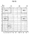
- the fourth mask M4 covers areas in memory cells, in which the fourteenth horizontal area n up to and including the twenty-first horizontal area u with the first vertical range 1 up to and including that fifth vertical area 5 overlap, and areas in which the fourth horizontal range d up to and including the tenth horizontal area j with the first vertical Range 1 through the fifth vertical range 5 overlap, and areas where the fourteenth horizontal range n up to and including the seventeenth horizontal area q with the sixth vertical area 6 and the seventh vertical area 7 intersect, and areas in which the fourth horizontal range d to including the seventh horizontal area g with the sixth vertical area 6 and the seventh vertical area 7 overlap, and areas where the eleventh horizontal Range k up to and including the seventeenth horizontal Area q with the eighth vertical area 8 and the ninth vertical area 9 intersect, and areas in which the first horizontal area a to inclusive the seventh horizontal area g with the eighth vertical area Intersect area 8 and the ninth vertical area 9, not starting.
- a fifth mask (not shown) made of photoresist, rectangular, approximately 150 nm deep p-doped regions are produced within the second wells Wa2.
- the dopant concentration of the rectangular areas is approx. 5 * 10 20 cm -3 .
- the p-doped regions are suitable as first source / drain regions 3 S / D1 of third transistors and first source / drain regions 4 S / D1 of fourth transistors (see FIG. 2).
- the fifth mask covers areas where the fourteenth horizontal range n through the twentieth horizontal area t with the eleventh vertical area 11 through the thirteenth vertical region 13 overlap, and areas where the third is horizontal Range c up to and including the tenth horizontal Area j with the eleventh vertical area 11 through inclusive intersect the thirteenth vertical region 13, not starting.
- a first insulating layer (not shown) is then produced by depositing SiO 2 in a thickness of approximately 100 nm.
- An approximately 100 nm thick conductive layer S1 is produced over the first insulating layer by depositing doped polysilicon.
- a second insulating layer (not shown) is produced over the conductive layer S1 by depositing SiO 2 in a thickness of approximately 100 nm (see FIG. 3).
- first trenches G1, second trenches G2 and fourth trenches G4 about 500 nm deep (see FIG. 3 ).
- the depth of the first trenches G1, the second trenches G2 and the fourth trenches G4 from the surface O is approximately 500 nm.
- the first trenches G1 and the second trenches G2 run within the first troughs Wa1.
- the fourth trenches G4 run within the second troughs Wa2.
- a second insulating structure I2 arises from the first insulating layer, and a preliminary structure VS arises from the second insulating layer.
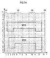
- the sixth mask M6 in each case covers the memory cells the first vertical area 1, the sixth vertical area 6, the seventh vertical region 7 and the thirteenth vertical area 13 does not decrease.
- a seventh mask M7 made of photoresist (see Fig. 7c) and an eighth mask M8 made of photoresist (see Fig. 7d) are through oblique implantation on second flanks 1F2 of the first trenches G1 on first flanks 2F1 of the second trenches G2 and on the second Flanks 2F2 of the second trenches G2 p-doped first channel stop regions C1 generates (see Fig. 3).
- the seventh mask M7 covers in the memory cells the second tub Wa2, as well as areas where the eighteenth horizontal range r through the twentieth horizontal area t with the first vertical area 1 intersect up to and including the eighth vertical area 8, and areas where the eighth horizontal Range h up to and including the tenth horizontal range j with the first vertical range 1 up to and including that eighth vertical area 8 overlap.
- the eighth mask M8 covers the second tub Wa2 in the memory cell as well as areas in which the eighth horizontal area h up to and including the tenth horizontal area j with the first vertical area 1 and the second vertical area 2 overlap, and areas where the eighteenth horizontal range r through the twentieth horizontal area t with the first vertical area 1 and overlap the second vertical area 2, and areas in which the fourteenth horizontal area n up to and including the sixteenth horizontal area p the seventh vertical area 7 through the ninth inclusive intersect vertical area 9, and areas where the third horizontal area c up to and including the sixth horizontal area f with the seventh vertical Area 7 through the ninth vertical area 9 overlap, from.
- the ninth mask in the memory cells covers each first tubs Wa1 as well as areas where the eighteenth horizontal range r up to and including the twentieth horizontal Area t with the twelfth vertical area 12 and intersect the thirteenth vertical region 13, and Areas in which the eighth horizontal area h to including the tenth horizontal area j with the twelfth vertical area 12 and the thirteenth vertical area Overlap area 13, from.
- the first channel stop regions C1 and the second channel stop regions C2 jointly form channel stop regions C.
- the dopant concentration of the channel stop regions C is approximately 10 19 cm -3 and is greater than the dopant concentration first tubs Wa1 and the second tubs Wa2. Due to their high dopant concentration, the channel stop regions C prevent a current flow between adjacent source / drain regions.
- the tenth mask in the memory cells covers areas in which the seventeenth horizontal area q up to and including the twenty-first horizontal area u overlap with the fourth vertical area 4 up to and including the eighth vertical area 8, and areas in which the seventh horizontal area Do not overlap area g through the eleventh horizontal area k with the fourth vertical area 4 through the eighth vertical area 8.
- the diffusion areas are divided into first diffusion areas and second diffusion areas D2 (see FIG. 3).
- the first diffusion regions adjoin the second source / drain regions 1 S / D2 of the first transistors, and the second diffusion regions D2 adjoin the second source / drain regions 2 S / D2 of the second transistors.
- the dopant concentration of the diffusion areas is high and is approximately 10 20 cm -3 .
- SiO 2 is deposited in a thickness of approximately 80 nm in a TEOS process and etched back in order to on the first flanks of the first trenches G1, on the second flanks 1F2 of the first trenches G1, on the first flanks 2F1 of the second trenches G2, to produce spacers Sp on the second flanks 2F2 of the second trenches G2, on the first flanks 4F1 of the fourth trenches G4 and on the second flanks of the fourth trenches G4.
- n-doped first conductive structures L1 are produced (see FIG Fig. 3).
- the first conductive structures L1 run along the bottoms of the first trenches G1 and are connected to a first voltage connection. Parts of the first conductive structures L1 are suitable as first source / drain regions of the first transistors and as first source / drain regions 2 S / D1 of the second transistors (see FIG. 3).
- the eleventh mask M11 covers each in the memory cells the first trench G1 and areas where the fourteenth horizontal range n through the twentieth horizontal area t with the third vertical area 3 intersect up to and including the eighth vertical area 8, and rectangular areas where the third horizontal range c up to and including the tenth horizontal Area j with the third vertical area 3 through inclusive intersect the eighth vertical area 8, not starting.
- the first source / drain regions 5 are S / D1 of the fifth transistors from the first source / drain regions 6 S / D1 of the sixth transistors isolated.
- p-doped second conductive structures L2 are produced by implantation on the bottoms of the fourth trenches G4 (see FIG. 3).
- the dopant concentration of the second conductive structures L2 is approximately 5 * 10 20 cm -3 .
- the second conductive structures L2 are connected to a second voltage connection. Parts of the second conductive structure L2 are suitable as second source / drain regions of the third transistors and as second source / drain regions 4 S / D2 of the fourth transistors.
- the first source / drain regions 5 S / D1 fifth transistor When generating the first source / drain regions 5 S / D1 fifth transistor, the first source / drain regions 6 S / D1 the sixth transistors, the first conductive structures L1 and the second conductive structures L2 prevent the provisional Structure VS and the Spacer Sp the implantation of others Parts of the memory cells.
- a gate dielectric Gd is then generated by thermal oxidation (see FIG. 4).
- doped polysilicon is deposited in a thickness of approximately 40 nm and etched back to the extent that the polysilicon is arranged in the form of spacers below the flanks of the structured conductive layer S1. It is then etched with, for example, HF SiO 2 in such a way that the flanks of the structured conductive layer S1 are exposed.
- Doped polysilicon is deposited to a thickness of approximately 80 nm and etched back, causing the flanks of the first Trenches G1, the second trenches G2 and the fourth trenches G4 Spacers are created that form the structured conductive layer S1 to contact.
- Silicon is etched using a thirteenth mask M13 made of photoresist (see FIG. 7f), so that parts of the spacers are removed.
- C 2 F 6 + O 2 is suitable as an etchant. This results in first gate electrodes of the first transistors, second gate electrodes Ga2 of the second transistors, third gate electrodes of the third transistors, fourth gate electrodes Ga4 of the fourth transistors and third conductive structures L3 which are arranged on the first flanks 2F1 of the second trenches G2 (see FIG. 4 ).
- Spacers which are arranged on the second flanks 2F2 of the second trenches G2 are not etched and are suitable as word lines W. Parts of the word lines W are suitable as fifth gate electrodes Ga5 of the fifth transistors and as sixth gate electrodes of the sixth transistors.
- the thirteenth mask M13 covers in the memory cells Areas in which the fifteenth horizontal area o up to and including the seventeenth horizontal area q with the first vertical area 1 and the second vertical Area 2 overlap and areas where there is the fifteenth horizontal range up to and including the seventeenth horizontal area q with the twelfth vertical Intersect area 12 and the thirteenth vertical area 13, and areas where the first horizontal Area a through the seventh horizontal area g inclusive with the first vertical area 1 and the second vertical Overlap area 2 and areas where the first horizontal area a through the fourth horizontal Area d with the third vertical area 3 to including the sixth vertical area 6 overlap, and areas where the first horizontal area a up to and including the seventh horizontal area g with the twelfth vertical region 12 and the thirteenth overlap vertical area 13, not from.
- first horizontal conductive structures H1, second horizontal conductive structures H2, third horizontal conductive structures, fourth horizontal conductive structures H4 and fifth horizontal ones are produced by etching silicon from the structured conductive layer S1 conductive structures H5 (see Fig. 4, 6b, 6d).
- C 2 F 6 + O 2 is suitable as an etchant.
- the fourteenth mask M14 covers areas in which the eighteenth horizontal range r up to and including the twenty-second horizontal area v with the first vertical Ranges 1 through the sixth vertical Overlap area 6 and areas where the twelfth horizontal range 1 through the fourteenth inclusive horizontal area n with the first vertical area 1 through the fourth vertical region 4 overlap, and areas where the eighteenth is horizontal R ranges up to and including the twenty-second horizontal area v with the eleventh vertical area 11 up to and including the thirteenth vertical region 13 overlap, and areas where the twelfth horizontal Range 1 through the fourteenth horizontal Area n with the eleventh vertical area 11 through inclusive intersect the thirteenth vertical region 13, and areas in which the fifth horizontal area e up to and including the eighth horizontal area h with the fourth vertical range 4 up to and including that overlap the sixth vertical area 6.
- the first horizontal conductive structures H1 adjoin the first Gate electrodes Ga1 of the first transistors and to the third conductive structures L3.
- the second horizontal conductive Structures H2 adjoin the second gate electrodes Ga2 of the second transistors.
- the third horizontal conductive structures adjoin the third gate electrodes Ga3 of the third transistors.
- the fourth horizontal conductive structures H4 adjoin the fourth gate electrodes Ga4 of the fourth transistor.
- the fifth horizontal conductive structures H5 adjoin the third conductive ones Structures L3.
- SiO 2 is deposited to a thickness of approximately 600 nm.
- 500 nm of SiO 2 is removed and planarized, which creates a third insulating structure I3 (see FIG. 5).
- second contacts K2 which contact the second source / drain regions 1 S / D2 of the first transistors
- fourth contacts which contact the first source / drain regions 3 S / D1 of the third transistors
- fifth contacts K5 contacting the second source / drain regions 2 S / D2 of the second transistors
- sixth contacts contacting the first source / drain regions 4 S / D1 of the fourth transistors is made of photoresist using a fifteenth mask (not shown) SiO 2 selectively etched to silicon until parts of the source / drain regions are exposed.
- CHF 3 + O 2 is suitable as an etchant.
- the fifteenth mask in each case covers the memory cells Areas in which the thirteenth horizontal area m up to and including the fifteenth horizontal area o the second vertical area 2 through the fourth inclusive vertical area 4 intersect, and areas where the fifth horizontal area e up to and including the eighth horizontal area h with the third vertical Range 3 through the fifth vertical range 5 overlap, and areas where the thirteenth horizontal Range m up to and including the fifteenth horizontal Area o with the twelfth vertical area 12 overlap, and areas where the third is horizontal Range c up to and including the sixth horizontal Intersect area f with the twelfth vertical area 12, not starting.
- tungsten is deposited to a thickness of approximately 200 nm, which results in the second contacts K2, the fourth contacts K4, the fifth contacts K5 and the sixth contacts (see FIGS. 5, 6b).
- a sixteenth mask M16 made of photoresist is used to etch tungsten, which results in fifth conductive structures L5 and sixth conductive structures L6 (see FIGS. 5, 6b).
- SF 6 for example, is suitable as an etchant.
- the fifth conductive structures L5 each adjoin a second contact K2 and a fourth contact K4.
- the sixth conductive structures L6 each adjoin a fifth contact K5 and a sixth contact.
- the sixteenth mask M16 covers in the memory cells a first U-shaped area and a second U-shaped Range.
- the first U-shaped area consists of Areas in which the thirteenth horizontal area m up to and including the seventeenth horizontal area q the second vertical area 2 through the fourth inclusive vertical area 4 intersect, and areas where the fifteenth horizontal range o up to and including the seventeenth horizontal area q with the fifth vertical range 5 through the eleventh vertical Area 11 overlap and areas where the thirteenth horizontal range m up to and including the seventeenth horizontal area q with the twelfth vertical area 12 overlap.
- the second U-shaped area exists from areas in which the fourth horizontal area d up to and including the ninth horizontal area i with the third vertical area 3 through the fifth vertical area 5 intersect, and areas where the seventh horizontal range g up to and including the ninth horizontal area i with the sixth vertical area 6 up to and including the eleventh vertical region 11 overlap, and areas where the third is horizontal Range c up to and including the ninth horizontal Overlap area i with the twelfth vertical area 12.
- Boron phosphor glass is deposited in a thickness of approx. 600 nm. With the help of chemical-mechanical polishers, the borophosphorus glass is planarized, which creates a fourth insulating structure I4 (see FIG. 6a).
- first contacts K1 which contact the second source / drain regions 1 S / D2 of the first transistors
- third contacts which contact the first source / drain regions 3 S / D1 of the third transistors
- seventh contacts K7 contacting the second source / drain regions 5 S / D2 of the fifth transistor
- eighth contacts contacting the second source / drain regions 6 S / D2 of the sixth transistors is carried out using a seventeenth mask (not shown)
- Photoresist borophosphorus glass is selectively etched to silicon until parts of the source / drain regions are exposed.
- C 2 F 6 + O 2 is suitable as an etchant.
- the seventeenth mask in each case covers the memory cells Areas in which the nineteenth horizontal area s up to and including the twenty-first horizontal area u with the second vertical area 2 up to and including that fourth vertical area 4 intersect, and areas in which are the nineteenth horizontal range s up to and including the twenty-first horizontal area u with overlap the twelfth vertical area 12, and areas in which the eleventh horizontal range k up to and including the thirteenth horizontal area m with the ninth vertical area 9 intersect, and areas in which the second horizontal area b up to and including fifth horizontal area e with the ninth vertical area 9 overlap, not off.
- tungsten is in 300 nm thick and etched back, whereby the first contacts K1, the third contacts, the seventh Contacts K7 and the eighth contacts are created (see Fig. 6b, 6d).
- AlSiCu is deposited in a thickness of approx. 500 nm and structured with an eighteenth mask M18 made of photoresist (see FIG. 7i) by an etching step.
- BCl 3 + Cl 2 + N 2 + CH 4 is suitable as an etchant.
- a fourth conductive structure L4 adjoins a first contact K1 and a third contact.
- the first bit lines B1 are strip-shaped, run perpendicular to the first trenches G1 and adjoin the seventh contacts K7.
- the second bit lines B2 are essentially strip-shaped, run parallel to the first bit lines B1 and adjoin the eighth contacts.
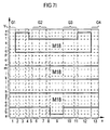
- the eighteenth mask M18 in the memory cells covers Areas in which the seventeenth horizontal area q up to and including the twenty-first horizontal Area u with the second vertical area 2 through inclusive intersect the fourth vertical area 4, and areas in which the seventeenth horizontal area q up to and including the nineteenth horizontal area s with the fifth vertical range 5 up to and including that eleventh vertical area 11 overlap, and areas in which are the seventeenth horizontal range q up to and including the twenty-first horizontal area u with intersect the twelfth vertical region 12, the eleventh horizontal area k, the twelfth horizontal area 1, the thirteenth horizontal area m, the fourth horizontal area Area d, the fifth horizontal area e, the sixth horizontal area f, the seventh horizontal area g and areas where the second horizontal Area b and the third horizontal area c with the ninth intersect vertical area 9, from.
- the dimensions of the layers, areas, areas and trenches described can be adapted to the respective requirements.
- Structures and layers made of SiO 2 can be produced in particular by thermal oxidation or by a deposition process.
- Polysilicon can be doped both during and after the deposition.
- doped polysilicon for example, metal silicides and / or metals can also be used.
- metal silicides and / or metals can also be used.
Landscapes
- Semiconductor Memories (AREA)
Claims (10)
- Groupement de cellules RAM statiquecomprenant des cellules de mémoire qui comportent respectivement 6 transistors,dans lequel une première zone (1 S/D1) de source/drain d'un premier des transistors est reliée à une première zone (2 S/D1) de source/drain d'un deuxième des transistors et à une première borne de tension,dans lequel une deuxième zone (1 S/D2) de source/drain du premier transistor est reliée à une première zone (3 S/D1) de source/drain d'un troisième des transistors, à une première zone (5 S/D1) de source/drain d'un cinquième des transistors, à une électrode (Ga2) de grille du deuxième transistor et à une électrode (Ga4) de grille d'un quatrième des transistors,dans lequel une électrode (Ga1) de grille du premier transistor est reliée à une deuxième zone (2 S/D2) de source/drain du deuxième transistor, à une première zone (4 S/D1) de source/drain du quatrième transistor, à une électrode (Ga3) de grille du troisième transistor et à une première zone (6 S/D1) de source/drain d'un sixième des transistors,dans lequel une deuxième zone (3 S/D2) de source/drain du troisième transistor est reliée à une deuxième zone (4 S/D2) de source/drain du quatrième transistor et à une deuxième borne de tension,dans lequel une deuxième zone (5 S/D2) de source/drain du cinquième transistor est reliée à une première ligne (B1) de bits,dans lequel une électrode (Ga5) de grille du cinquième transistor est reliée à une électrode (Ga6) de grille du sixième transistor et à une ligne (W) de mots,dans lequel une deuxième zone (6 S/D2) de source/drain du sixième transistor est reliée à une deuxième ligne (B2) de bits,dans lequel le troisième transistor et le quatrième transistor sont complémentaires du premier transistor, du deuxième transistor, du cinquième transistor et du sixième transistor,dans lequel les six transistors sont constitués sous la forme de transistors MOS verticaux,dans lequel le premier transistor et le deuxième transistor sont placés sur un deuxième flanc (1F2) d'un premier sillon (G1) qui s'étend dans un substrat (S),dans lequel le cinquième transistor et le sixième transistor sont disposés sur un deuxième flanc (2F2) d'un deuxième sillon (G2) qui s'étend dans le substrat (S) et parallèlement au premier sillon (G1),dans lequel le troisième transistor et le quatrième transistor sont disposés sur un premier flanc (4F1) d'un quatrième sillon (G4) qui s'étend dans le substrat (S) et parallèlement au deuxième sillon (G2),dans lequel la ligne (W) de mots s'étend le long du deuxième flanc (2F2) du deuxième sillon (G2),dans lequel une première structure (L1) conductrice est reliée à la première borne de tension et une deuxième structure (L2) conductrice à la deuxième borne de tension,dans lequel la première structure (L1) conductrice s'étend le long du premier sillon (G1) et la deuxième structure (L2) conductrice le long du quatrième sillon (G4),dans lequel la première ligne (B1) de bits et la deuxième ligne (B2) de bits s'étendent transversalement à la ligne (W) de mots et parallèlement entre elles,dans lequel la première zone (1 S/D1) de source/drain du premier transistor et la première zone (2 S/D1) de source/drain du deuxième transistor sont reliées à la première structure (L1) conductrice,dans lequel la deuxième zone (3 S/D2) de source/drain du troisième transistor et la deuxième zone (4 S/D2) de source/drain du quatrième transistor sont reliées à la deuxième structure (L2) conductrice.
- Groupement de cellules de mémoire RAM statique suivant la revendication 1, dans lequel des électrodes de grille ou des structures conductrices sont voisines de structures conductrices horizontales qui sont disposées à l'extérieur du premier sillon (G1), du deuxième sillon (G2), et du quatrième sillon (G4) au-dessus d'une surface (O) du substrat (S) et par lesquelles elles sont mises en contact.
- Groupement de cellules de mémoire RAM statique suivant la revendication 2,dans lequel le premier sillon (G1) et le deuxième sillon (G2) sont disposés dans une première cuvette (Wa1) du substrat (S) dopée suivant un deuxième type de conductivité,dans lequel le quatrième sillon (G4) est disposé dans une deuxième cuvette (Wa2) du substrat (S) dopée suivant un type de conductivité opposé au deuxième type de conductivité,dans lequel la première structure (L1) conductrice est voisine au sein du substrat d'un fond du premier sillon (G1) et est dopée suivant le premier type de conductivité, et la deuxième structure conductrice est voisine au sein du substrat (S) d'un fond du quatrième sillon (G4) et est dopée suivant le deuxième type de conductivité,dans lequel la première zone (1 S/D1) de source/drain du premier transistor et la première zone (2 S/D1) de source/drain du deuxième transistor font partie de la première structure (L1) conductrice,dans lequel la deuxième zone (3 S/D2) de source/drain du troisième transistor et la deuxième zone (4 S/D2) de source/drain du quatrième transistor font partie de la deuxième structure (L2) conductrice,dans lequel il est disposé des parties d'une deuxième structure (I2) isolante entre des structures (H1, H2, H4, H5) conductrices horizontales et la surface (O),dans lequel l'électrode (Ga1) de grille du premier transistor, l'électrode (Ga2) de grille du deuxième transistor, l'électrode (Ga3) de grille du troisième transistor, l'électrode (Ga4) de grille du quatrième transistor, l'électrode (Ga5) de grille du cinquième transistor et l'électrode (Ga6) de grille du sixième transistor sont constituées sous la forme d'espaceur,dans lequel l'électrode (Ga1) de grille du premier transistor est voisine d'une première structure (H1) conductrice horizontale, l'électrode (Ga2) de grille du deuxième transistor est voisine d'une deuxième structure (H2) conductrice horizontale, l'électrode (Ga3) de grille du troisième transistor est voisine d'une troisième structure conductrice horizontale et l'électrode (Ga4) de grille du quatrième transistor est voisine d'une quatrième structure (H4) conductrice horizontale,dans lequel la ligne (W) de mots est constituée sous la forme d'espaceur sur le deuxième flanc (2F2) du deuxième sillon (G2),dans lequel l'électrode (Ga5) de grille du cinquième transistor et l'électrode (Ga6) de grille du sixième transistor font partie de la ligne (W) de mots,dans lequel une troisième structure (L3) conductrice est constituée sous la forme d'un espaceur sur le premier flanc (2F1) du deuxième sillon (G2),dans lequel la troisième structure (L3) conductrice est voisine de la première structure (H1) conductrice horizontale et de la cinquième structure (H5) conductrice horizontale,dans lequel le deuxième flanc (1F2) du premier sillon (G1), le premier flanc (2F1) du deuxième sillon (G2), le deuxième flanc (2F2) du deuxième sillon (G2) et le premier flanc (4F1) du quatrième sillon (G4) sont munis d'un diélectrique (Gd) de grille,dans lequel la deuxième zone (1 S/D2) de source/drain du premier transistor et la deuxième zone (2 S/D2) de source/drain du deuxième transistor sont voisines de la surface (O) ainsi que du deuxième flanc (1F2) du premier sillon (G1) et du premier flanc (2F1) du deuxième sillon (G2),dans lequel la première zone (3 S/D1) de source/drain du troisième transistor et la première zone (4 S/D1) de source/drain du quatrième transistor sont voisines de la surface (O) ainsi que du premier flanc (4 F1) du quatrième transistor (G4),dans lequel la deuxième zone (5 S/D2) de source/drain du cinquième transistor et la deuxième zone (6 S/D2) de source/drain du sixième transistor sont voisines de la surface (O) ainsi que du deuxième flanc (2F2) du deuxième sillon (G2),dans lequel la première structure (H1) conductrice horizontale est reliée à une quatrième structure (L4) conductrice par un premier contact (K1),dans lequel la troisième structure conductrice horizontale est reliée à la quatrième structure (L4) conductrice par un troisième contact (K3),dans lequel la quatrième structure (L4) conductrice est disposée au-dessus des deuxièmes structures (H1, H2, H4, H5) conductrices horizontales,dans lequel la deuxième zone (1 S/D2) de source/drain du premier transistor est reliée par un deuxième contact (K2) à la deuxième structure (H2) conductrice horizontale et à une cinquième structure (L5) conductrice,dans lequel la cinquième structure (L5) conductrice est disposée au-dessus des structures (H1, H2, H4, H5) conductrices horizontales et en dessous de la quatrième structure (L4) conductrice,dans lequel la première zone (3 S/D1) de source/drain du troisième transistor est reliée par un quatrième contact (K4) à la quatrième structure (H4) conductrice horizontale et à la cinquième structure (L5) conductrice,dans lequel la deuxième zone (2 S/D2) de source/drain du deuxième transistor est reliée par un cinquième contact (K5) à la cinquième structure (H5) conductrice horizontale et à une sixième structure (L6) conductrice,dans lequel le niveau de la sixième structure (L6) conductrice suivant un axe perpendiculaire à la surface (O) correspond au niveau de la cinquième structure (L5) conductrice,dans lequel la première zone (4 S/D1) de source/drain du quatrième transistor est reliée par un sixième contact (K6) à la sixième structure (L6) conductrice,dans lequel la deuxième zone (5 S/D2) de source/drain du cinquième transistor est reliée par un septième contact (K7) à la première ligne (B1) de bits, et la deuxième zone (6 S/D2) de source/drain du sixième transistor est reliée par un huitième contact (K8) à la deuxième ligne (B2) de bits,dans lequel une première zone de diffusion dopée suivant le premier type de conductivité est voisine au sein du substrat (S) du premier flanc (2F1) du deuxième sillon (G2), de la deuxième zone (1 S/D1) de source/drain du premier transistor et de la première zone (5 S/D1) de source/drain du cinquième transistor,dans lequel une deuxième zone (D2) de diffusion dopée suivant le premier type de conductivité est voisine au sein du substrat (S) du premier flanc (2F1) du deuxième sillon (G2), de la deuxième zone (2 S/D2) de source/drain du deuxième transistor et de la première zone (6 S/D1) de source/drain du sixième transistor.
- Groupement de cellules de mémoire RAM statique suivant les revendications 1, 2 et/ou 3,dans lequel il est disposé, au sein du substrat (S), sur des parties des flancs des sillons dont ne sont pas voisines des électrodes de grille et des zones de diffusion, des zones (C) de Channel-Stop qui sont très dopées,dans lequel une première structure (I1) d'isolement en forme de bande s'étend parallèlement au deuxième sillon (G2) et au quatrième sillon (G4) et entre ceux-ci.
- Groupement de cellules de mémoire RAM statique suivant l'une des revendications 1 à 4, dans lequel des cellules de mémoire voisines le long de la première ligne (B1) de bits sont disposées symétriques les unes des autres comme en un miroir par rapport à un axe qui s'étend le long d'une ligne médiane d'un premier sillon (G1) ou d'un quatrième sillon (G4).
- Procédé de fabrication d'un groupement de cellules de mémoires RAM statique,dans lequel on produit des cellules de mémoire qui comprennent respectivement un premier transistor, un deuxième transistor, un troisième transistor, un quatrième transistor, un cinquième transistor et un sixième transistor,dans lequel on produit des lignes (W) de mots, des premières lignes (B1) de bits et des deuxièmes lignes (B2) de bits,dans lequel on produit des électrodes de grille, des premières zones de source/drain et des deuxièmes zones de source/drain,dans lequel on relie une première zone (1 S/D1) de source/drain du premier transistor à une première zone (2 S/D1) de source/drain du deuxième transistor et à une borne de tension,dans lequel on relie une deuxième zone (1 S/D2) de source/drain du premier transistor à une première zone (3 S/D1) de source/drain du troisième transistor, à une première zone (5 S/D1) de source/drain du cinquième transistor, à une électrode (Ga2) de grille du deuxième transistor et à une électrode (Ga4) de grille du quatrième transistor,dans lequel on relie une électrode (Ga1) de grille du premier transistor à une deuxième zone (2 S/D2) de source/drain du deuxième transistor, à une première zone (4 S/D1) de source/drain du quatrième transistor, à une électrode (Ga3) de grille du troisième transistor et à une première zone (6 S/D1) de source/drain d'un sixième transistor,dans lequel on relie une deuxième zone (3 S/D2) de source/drain du troisième transistor à une deuxième zone (4 S/D2) de source/drain du quatrième transistor et à une deuxième borne de tension,dans lequel on relie une deuxième zone (5 S/D2) de source/drain du cinquième transistor à une première ligne (B1) de bits,dans lequel on relie une électrode (Ga5) de grille du cinquième transistor à une électrode (Ga6) de grille du sixième transistor et à une ligne (W) de mots,dans lequel on relie une deuxième zone (6 S/D2) de source/drain du sixième transistor à une deuxième ligne (B2) de bits,dans lequel on constitue le troisième transistor et le quatrième transistor sous la forme de transistors complémentaires du premier transistor, du deuxième transistor, du cinquième transistor et du sixième transistor,dans lequel on forme les six transistors sous la forme de transistors MOS verticaux,dans lequel on produit, dans un substrat (S), des premiers sillons (G1), des deuxièmes sillons (G2) et des quatrièmes sillons (G4) qui s'étendent sensiblement parallèlement entre eux,dans lequel on munit des flancs des premiers sillons (G1), des deuxièmes sillons (G2) et des quatrièmes sillons (G4) d'un diélectrique (Gd) de grille,dans lequel on forme le premier transistor et le deuxième transistor au voisinage du deuxième flanc (1F2) d'un premier sillon (G1),dans lequel on forme le cinquième transistor et le sixième transistor au voisinage d'un deuxième flanc (2F2) d'un deuxième sillon (G2),dans lequel on forme le troisième transistor et le quatrième transistor au voisinage d'un premier flanc (4F1) d'un quatrième sillon (G4),dans lequel on forme la ligne (W) de mots le long du deuxième flanc (2F2) du deuxième sillon (G2),dans lequel on forme, le long du premier sillon (G1), une première structure (L1) conductrice que l'on relie à la première borne de tension,dans lequel on produit le long du quatrième sillon (G4) une deuxième structure (L2) conductrice que l'on relie à la deuxième borne de tension,dans lequel on forme, transversalement à la ligne (W) de mots, la première ligne (B1) de bits et, parallèlement à la première ligne (B1) de bits, la deuxième ligne (B2) de bits,dans lequel on relie la première zone (1 S/D1) de source/drain du premier transistor et la première zone (2 S/D1) de source/drain du deuxième transistor à la première structure (L1) conductrice,dans lequel on relie la deuxième zone (3 S/D2) de source/drain du troisième transistor et la deuxième zone (4 S/D2) de source/drain du quatrième transistor à la deuxième structure (L2) conductrice.
- Procédé suivant la revendication 6, dans lequel, pour établir le contact d'électrodes de grille ou de structures conductrices, on produit à l'extérieur du premier sillon (G1), du deuxième sillon (G2) et du quatrième sillon (G4), au-dessus d'une surface (O) de substrat (S), des structures conductrices horizontales, de façon à ce que les structures conductrices horizontales soient voisines respectivement d'une électrode de grille ou/et d'une structure conductrice.
- Procédé suivant la revendication 7,dans lequel on produit à la surface (O), par implantation, la deuxième zone (1 S/D2) de source/drain du premier transistor, la deuxième zone (2 S/D2) de source/drain du deuxième transistor, la deuxième zone (5 S/D2) de source/drain du cinquième transistor, la deuxième zone (6 S/D2) de source/drain du sixième transistor, la première zone (3 S/D1) de source/drain du troisième transistor et la première zone (4 S/D1) de source/drain du quatrième transistor,dans lequel on produit ensuite les premiers sillons (G1), les deuxièmes sillons (G2) et les quatrièmes sillons (G4),dans lequel on produit la deuxième zone (1 S/D2) de source/drain du premier transistor, la deuxième zone (2 S/D2) de source/drain du deuxième transistor, la deuxième zone (5 S/D2) de source/drain du cinquième transistor, la deuxième zone (6 S/D2) de source/drain du sixième transistor, la première zone (3 S/D1) de source/drain du troisième transistor et la première zone (4 S/D1) de source/drain du quatrième transistor, les premiers sillons (G1), les deuxièmes sillons (G2) et les quatrièmes sillons (G4), de façon à ce que la deuxième zone (1 S/D2) de source/drain du premier transistor et la deuxième zone (2 S/D2) de source/drain du deuxième transistor soient voisines du deuxième flanc (1F2) du premier sillon (G1) et du premier flanc (2F1) du deuxième sillon (G2), et de façon à ce que la deuxième zone (5 S/D2) de source/drain du cinquième transistor et la deuxième zone (6 S/D2) de source/drain du sixième transistor soient voisines du deuxième flanc (2F2) du deuxième sillon (G2), et de façon à ce que la première zone (3 S/D1) de source/drain du troisième transistor et la première zone (4 S/D1) de source/drain du quatrième transistor soient voisines du premier flanc (4F1) du quatrième sillon (4),dans lequel on produit, par implantation inclinée, une première région de diffusion voisine de la deuxième zone (1 S/D2) de source/drain du premier transistor sur le premier flanc (2F1) du deuxième sillon (G2) au sein du substrat (S),dans lequel on produit, par implantation inclinée, une deuxième région (D2) de diffusion voisine de la deuxième zone (2 S/D2) de source/drain du deuxième transistor sur le premier flanc (2F1) du deuxième sillon (G2) au sein du substrat (S)dans lequel on produit, par implantation, au sein du substrat (S) la première structure (L1) conductrice dopée suivant le premier type de conductivité sur un fond du premier sillon (G1),dans lequel on produit, par implantation sur un fond du deuxième sillon (G2), la première zone (5 S/D1) de source/drain du cinquième transistor et la première zone (6 S/D1) de source/drain du sixième transistor,dans lequel on produit, par implantation sur un fond du quatrième sillon (G4), la deuxième structure (L2) conductrice dopée suivant un deuxième type de conductivité opposé au premier type de conductivité,dans lequel on produit par dépôt, attaque en retrait et attaque masquée de matériau conducteur sur le deuxième flanc (2F2) du deuxième sillon (G2) la ligne (W) de mots, sur le deuxième flanc (1F2) du premier sillon(G1) l'électrode (Ga1) de grille du premier transistor et l'électrode (Ga2) de grille du deuxième transistor, sur le premier flanc (2F1) du deuxième sillon (G2) une troisième structure (L3) productrice et sur le premier flanc (4F1) du quatrième sillon (G4) l'électrode (Ga3) de grille du troisième transistor et l'électrode (Ga4) de grille du quatrième transistor,dans lequel on produit, par dépôt de matériau isolant sur la surface (O), une deuxième structure (12) isolante,dans lequel on forme une couche (S1) conductrice par dépôt de matériau conducteur sur la deuxième structure (12) isolante,dans lequel on produit, par attaque de matériau conducteur à l'aide d'un quatorzième masque (M14), une première structure (H1) conductrice horizontale, une deuxième structure (H2) conductrice horizontale, une troisième structure conductrice horizontale, une quatrième structure (H4) conductrice horizontale et une cinquième structure (H5) conductrice horizontale,dans lequel, par dépôt et attaque en retour de matériau isolant, on produit une troisième structure (13) isolante,dans lequel on produit un deuxième contact (K2) qui est voisin de la deuxième zone (1 S/D2) de source/drain du premier transistor, un cinquième contact (K2) qui est voisin de la deuxième zone (2 S/D2) de source/drain du deuxième transistor, un quatrième contact (K4) qui est voisin de la première zone (3 S/D1) de source/drain du troisième transistor, un sixième contact (K6) qui est voisin de la première zone (4 S/D1) de source/drain du quatrième transistor, une cinquième structure (L5) conductrice qui est voisine du deuxième contact (K2) et du quatrième contact (K4) et une sixième structure (L6) conductrice qui est voisine du cinquième contact (K5) et du sixième contact (K6), en attaquant du matériau isolant à l'aide d'un quinzième masque (M15) et en déposant ensuite du matériau conducteur et en structurant à l'aide d'un seizième masque (M16),dans lequel on produit, par dépôt et attaque en retour de matériau isolant, une quatrième structure (I4) isolante,dans lequel on produit un premier contact (K1) qui est voisin de la première structure (H1) conductrice horizontale, un troisième contact (K3) qui est voisin de la troisième structure conductrice horizontale, un septième contact (K7) qui est voisin de la deuxième zone (5 S/D2) de source/drain du cinquième transistor, un huitième contact (K8) qui est voisin de la deuxième zone (6 S/D2) de source/drain du sixième transistor, une quatrième structure (L4) conductrice qui est voisine du premier contact (K1) et du troisième contact (K3), une première ligne (B1) de bits qui est voisine du septième contact (K7) et une deuxième ligne (B2) de bits qui est voisine du huitième contact (K8), en attaquant du matériau isolant à l'aide d'un dix-septième masque (M17) et en déposant ensuite du matériau conducteur et en le structurant à l'aide d'un dix-huitième masque (M18).
- Procédé suivant les revendications 6, 7 et/ou 8,dans lequel on produit des troisièmes sillons (G3) s'étendant parallèles entre eux et on les emplit de matériau isolant, ce qui produit de premières structures (11) isolantes,dans lequel on produit les deuxièmes sillons (G2) et les quatrièmes sillons (G4) de façon à ce qu'ils soient parallèles aux troisièmes sillons (G3) et de façon à ce que les troisièmes sillons (G3) se trouvent entre eux,dans lequel on produit, par implantation inclinée, des zones (C) de Channel-Stop très dopées sur des parties des flancs des sillons dont des électrodes de grille et des régions de diffusion ne sont pas voisines.
- Procédé suivant l'une des revendications 6 à 9, dans lequel on produit, le long de la première ligne (B1) de bits, des cellules de mémoire voisines qui sont symétriques comme en un miroir les unes des autres par rapport à un axe qui s'étend le long d'une ligne médiane d'un premier sillon (G1) ou d'un quatrième sillon (G4).
Applications Claiming Priority (3)
| Application Number | Priority Date | Filing Date | Title |
|---|---|---|---|
| DE19727472 | 1997-06-27 | ||
| DE19727472 | 1997-06-27 | ||
| PCT/DE1998/001551 WO1999000847A1 (fr) | 1997-06-27 | 1998-06-05 | Groupement de cellules de memoire ram statique et son procede de production |
Publications (2)
| Publication Number | Publication Date |
|---|---|
| EP0992068A1 EP0992068A1 (fr) | 2000-04-12 |
| EP0992068B1 true EP0992068B1 (fr) | 2003-09-03 |
Family
ID=7833897
Family Applications (1)
| Application Number | Title | Priority Date | Filing Date |
|---|---|---|---|
| EP98934869A Expired - Lifetime EP0992068B1 (fr) | 1997-06-27 | 1998-06-05 | Groupement de cellules de memoire ram statique et son procede de production |
Country Status (6)
| Country | Link |
|---|---|
| US (2) | US6222753B1 (fr) |
| EP (1) | EP0992068B1 (fr) |
| JP (1) | JP2002506575A (fr) |
| DE (1) | DE59809504D1 (fr) |
| TW (1) | TW429620B (fr) |
| WO (1) | WO1999000847A1 (fr) |
Families Citing this family (14)
| Publication number | Priority date | Publication date | Assignee | Title |
|---|---|---|---|---|
| DE19845003C1 (de) * | 1998-09-30 | 2000-02-10 | Siemens Ag | Vertikaler Feldeffekttransistor mit innenliegendem ringförmigen Gate und Herstellverfahren |
| DE19845004C2 (de) * | 1998-09-30 | 2002-06-13 | Infineon Technologies Ag | DRAM-Zellenanordnung und Verfahren zu deren Herstellung |
| US6459123B1 (en) * | 1999-04-30 | 2002-10-01 | Infineon Technologies Richmond, Lp | Double gated transistor |
| US6686604B2 (en) * | 2001-09-21 | 2004-02-03 | Agere Systems Inc. | Multiple operating voltage vertical replacement-gate (VRG) transistor |
| US6773994B2 (en) * | 2001-12-26 | 2004-08-10 | Agere Systems Inc. | CMOS vertical replacement gate (VRG) transistors |
| US6670642B2 (en) * | 2002-01-22 | 2003-12-30 | Renesas Technology Corporation. | Semiconductor memory device using vertical-channel transistors |
| US7138685B2 (en) * | 2002-12-11 | 2006-11-21 | International Business Machines Corporation | Vertical MOSFET SRAM cell |
| JP2004241397A (ja) * | 2003-01-23 | 2004-08-26 | Dainippon Printing Co Ltd | 薄膜トランジスタおよびその製造方法 |
| US20050167733A1 (en) * | 2004-02-02 | 2005-08-04 | Advanced Micro Devices, Inc. | Memory device and method of manufacture |
| KR100724560B1 (ko) * | 2005-11-18 | 2007-06-04 | 삼성전자주식회사 | 결정질 반도체층을 갖는 반도체소자, 그의 제조방법 및그의 구동방법 |
| US20070249133A1 (en) * | 2006-04-11 | 2007-10-25 | International Business Machines Corporation | Conductive spacers for semiconductor devices and methods of forming |
| JP2008177278A (ja) * | 2007-01-17 | 2008-07-31 | Toshiba Corp | スタティック型半導体記憶装置 |
| JP5469058B2 (ja) | 2008-04-16 | 2014-04-09 | ルネサスエレクトロニクス株式会社 | 半導体記憶装置 |
| US8581333B2 (en) | 2008-04-16 | 2013-11-12 | Renesas Electronics Corporation | Semiconductor device and method for manufacturing the same |
Family Cites Families (16)
| Publication number | Priority date | Publication date | Assignee | Title |
|---|---|---|---|---|
| US4453305A (en) * | 1981-07-31 | 1984-06-12 | The Secretary Of State For Defence In Her Britannic Majesty's Government Of The United Kingdom Of Great Britain And Northern Ireland | Method for producing a MISFET |
| US4890144A (en) | 1987-09-14 | 1989-12-26 | Motorola, Inc. | Integrated circuit trench cell |
| US4876215A (en) | 1987-07-02 | 1989-10-24 | Integrated Device Technology, Inc. | Method of making a static ram cell with trench pull-down transistors and buried-layer ground plate |
| US4835589A (en) | 1987-09-28 | 1989-05-30 | Motorola, Inc. | Ram cell having trench sidewall load |
| US5258635A (en) * | 1988-09-06 | 1993-11-02 | Kabushiki Kaisha Toshiba | MOS-type semiconductor integrated circuit device |
| US5016070A (en) | 1989-06-30 | 1991-05-14 | Texas Instruments Incorporated | Stacked CMOS sRAM with vertical transistors and cross-coupled capacitors |
| JPH03241865A (ja) | 1990-02-20 | 1991-10-29 | Texas Instr Japan Ltd | 半導体装置 |
| JPH04264770A (ja) | 1991-02-19 | 1992-09-21 | Sony Corp | 半導体メモリ |
| JPH04297067A (ja) | 1991-03-13 | 1992-10-21 | Mitsubishi Electric Corp | 半導体装置 |
| KR920022532A (ko) * | 1991-05-13 | 1992-12-19 | 문정환 | 이중 수직 채널을 갖는 스태틱램 및 그 제조방법 |
| JPH0575066A (ja) | 1991-09-13 | 1993-03-26 | Sony Corp | 半導体メモリ |
| US5285093A (en) | 1992-10-05 | 1994-02-08 | Motorola, Inc. | Semiconductor memory cell having a trench structure |
| US5324973A (en) | 1993-05-03 | 1994-06-28 | Motorola Inc. | Semiconductor SRAM with trench transistors |
| JP2601176B2 (ja) | 1993-12-22 | 1997-04-16 | 日本電気株式会社 | 半導体記憶装置 |
| JP2684979B2 (ja) | 1993-12-22 | 1997-12-03 | 日本電気株式会社 | 半導体集積回路装置及びその製造方法 |
| US5879971A (en) * | 1995-09-28 | 1999-03-09 | Motorola Inc. | Trench random access memory cell and method of formation |
-
1998
- 1998-05-29 TW TW087108397A patent/TW429620B/zh active
- 1998-06-05 EP EP98934869A patent/EP0992068B1/fr not_active Expired - Lifetime
- 1998-06-05 US US09/446,419 patent/US6222753B1/en not_active Expired - Lifetime
- 1998-06-05 JP JP50520399A patent/JP2002506575A/ja not_active Ceased
- 1998-06-05 DE DE59809504T patent/DE59809504D1/de not_active Expired - Lifetime
- 1998-06-05 WO PCT/DE1998/001551 patent/WO1999000847A1/fr not_active Ceased
-
2000
- 2000-11-09 US US09/708,636 patent/US6309930B1/en not_active Expired - Lifetime
Also Published As
| Publication number | Publication date |
|---|---|
| US6222753B1 (en) | 2001-04-24 |
| TW429620B (en) | 2001-04-11 |
| US6309930B1 (en) | 2001-10-30 |
| DE59809504D1 (de) | 2003-10-09 |
| EP0992068A1 (fr) | 2000-04-12 |
| WO1999000847A1 (fr) | 1999-01-07 |
| JP2002506575A (ja) | 2002-02-26 |
Similar Documents
| Publication | Publication Date | Title |
|---|---|---|
| DE19727466C2 (de) | DRAM-Zellenanordnung und Verfahren zu deren Herstellung | |
| DE4215708C2 (de) | SRAM und Verfahren zu dessen Herstellung | |
| DE19928781C1 (de) | DRAM-Zellenanordnung und Verfahren zu deren Herstellung | |
| DE69113579T2 (de) | Verfahren zur Herstellung einer DRAM-Zelle mit Stapelkondensator. | |
| EP0992068B1 (fr) | Groupement de cellules de memoire ram statique et son procede de production | |
| EP0744772A1 (fr) | Cellule de stockage DRAM à transistor vertical et son procédé de fabrication | |
| DE10362018A1 (de) | Anordnung und Verfahren zur Herstellung von vertikalen Transistorzellen und transistorgesteuerten Speicherzellen | |
| DE3787687T2 (de) | Halbleiterspeicher. | |
| EP0875937A2 (fr) | Réseau de cellules DRAM et son procédé de fabrication | |
| DE19845004C2 (de) | DRAM-Zellenanordnung und Verfahren zu deren Herstellung | |
| DE19911148C1 (de) | DRAM-Zellenanordnung und Verfahren zu deren Herstellung | |
| EP0917203A2 (fr) | Structure de type gain-cell pour DRAM et son procédé de manufacture | |
| DE19811882A1 (de) | DRAM-Zellenanordnung und Verfahren zu deren Herstellung | |
| DE10228717B4 (de) | Verfahren zum Isolieren aktiver Bereiche von Halbleiterspeicherelementen und zum Isolieren von Elementgebieten eines Halbleiterwafers | |
| EP1145319B1 (fr) | Circuit integre et son procede de fabrication | |
| WO2000019529A1 (fr) | Ensemble circuit integre comportant des transistors verticaux, et son procede de production | |
| DE19954867C1 (de) | DRAM-Zellenanordnung und Verfahren zu deren Herstellung | |
| EP1129482B1 (fr) | Procédé de production d'une configuration de cellules DRAM | |
| EP1125328B1 (fr) | Procede de production d'un ensemble de cellules de memoire ram dynamique | |
| DE19720193C2 (de) | Integrierte Schaltungsanordnung mit mindestens zwei vertikalen MOS-Transistoren und Verfahren zu deren Herstellung | |
| EP0862207A1 (fr) | Procédé de fabrication d'une capacité ensillonée de type DRAM | |
| DE19939589B4 (de) | Verfahren zur Herstellung eines Grabens mit vergrabener Platte | |
| EP0920060B1 (fr) | Réseau de cellules SRAM et méthode de fabrication | |
| DE19914490C1 (de) | Speicherzellenanordnung und Verfahren zu deren Herstellung | |
| DE19923262C1 (de) | Verfahren zur Erzeugung einer Speicherzellenanordnung |
Legal Events
| Date | Code | Title | Description |
|---|---|---|---|
| PUAI | Public reference made under article 153(3) epc to a published international application that has entered the european phase |
Free format text: ORIGINAL CODE: 0009012 |
|
| 17P | Request for examination filed |
Effective date: 19991217 |
|
| AK | Designated contracting states |
Kind code of ref document: A1 Designated state(s): DE FR GB IE IT |
|
| RAP1 | Party data changed (applicant data changed or rights of an application transferred) |
Owner name: INFINEON TECHNOLOGIES AG |
|
| GRAH | Despatch of communication of intention to grant a patent |
Free format text: ORIGINAL CODE: EPIDOS IGRA |
|
| GRAH | Despatch of communication of intention to grant a patent |
Free format text: ORIGINAL CODE: EPIDOS IGRA |
|
| GRAA | (expected) grant |
Free format text: ORIGINAL CODE: 0009210 |
|
| AK | Designated contracting states |
Kind code of ref document: B1 Designated state(s): DE FR GB IE IT |
|
| REG | Reference to a national code |
Ref country code: GB Ref legal event code: FG4D Free format text: NOT ENGLISH |
|
| REF | Corresponds to: |
Ref document number: 59809504 Country of ref document: DE Date of ref document: 20031009 Kind code of ref document: P |
|
| REG | Reference to a national code |
Ref country code: IE Ref legal event code: FG4D Free format text: GERMAN |
|
| GBT | Gb: translation of ep patent filed (gb section 77(6)(a)/1977) |
Effective date: 20031216 |
|
| ET | Fr: translation filed | ||
| PLBE | No opposition filed within time limit |
Free format text: ORIGINAL CODE: 0009261 |
|
| STAA | Information on the status of an ep patent application or granted ep patent |
Free format text: STATUS: NO OPPOSITION FILED WITHIN TIME LIMIT |
|
| 26N | No opposition filed |
Effective date: 20040604 |
|
| PGFP | Annual fee paid to national office [announced via postgrant information from national office to epo] |
Ref country code: GB Payment date: 20060615 Year of fee payment: 9 |
|
| PGFP | Annual fee paid to national office [announced via postgrant information from national office to epo] |
Ref country code: IE Payment date: 20060626 Year of fee payment: 9 |
|
| PGFP | Annual fee paid to national office [announced via postgrant information from national office to epo] |
Ref country code: IT Payment date: 20060630 Year of fee payment: 9 |
|
| GBPC | Gb: european patent ceased through non-payment of renewal fee |
Effective date: 20070605 |
|
| REG | Reference to a national code |
Ref country code: IE Ref legal event code: MM4A |
|
| PG25 | Lapsed in a contracting state [announced via postgrant information from national office to epo] |
Ref country code: IE Free format text: LAPSE BECAUSE OF NON-PAYMENT OF DUE FEES Effective date: 20070605 Ref country code: GB Free format text: LAPSE BECAUSE OF NON-PAYMENT OF DUE FEES Effective date: 20070605 |
|
| PG25 | Lapsed in a contracting state [announced via postgrant information from national office to epo] |
Ref country code: IT Free format text: LAPSE BECAUSE OF NON-PAYMENT OF DUE FEES Effective date: 20070605 |
|
| REG | Reference to a national code |
Ref country code: FR Ref legal event code: PLFP Year of fee payment: 18 |
|
| PGFP | Annual fee paid to national office [announced via postgrant information from national office to epo] |
Ref country code: FR Payment date: 20150619 Year of fee payment: 18 |
|
| PGFP | Annual fee paid to national office [announced via postgrant information from national office to epo] |
Ref country code: DE Payment date: 20150818 Year of fee payment: 18 |
|
| REG | Reference to a national code |
Ref country code: DE Ref legal event code: R119 Ref document number: 59809504 Country of ref document: DE |
|
| REG | Reference to a national code |
Ref country code: FR Ref legal event code: ST Effective date: 20170228 |
|
| PG25 | Lapsed in a contracting state [announced via postgrant information from national office to epo] |
Ref country code: FR Free format text: LAPSE BECAUSE OF NON-PAYMENT OF DUE FEES Effective date: 20160630 Ref country code: DE Free format text: LAPSE BECAUSE OF NON-PAYMENT OF DUE FEES Effective date: 20170103 |