EP0995199B1 - Dispositif electrique, appareil electrique et dispositif d'eclairage - Google Patents
Dispositif electrique, appareil electrique et dispositif d'eclairage Download PDFInfo
- Publication number
- EP0995199B1 EP0995199B1 EP98937547A EP98937547A EP0995199B1 EP 0995199 B1 EP0995199 B1 EP 0995199B1 EP 98937547 A EP98937547 A EP 98937547A EP 98937547 A EP98937547 A EP 98937547A EP 0995199 B1 EP0995199 B1 EP 0995199B1
- Authority
- EP
- European Patent Office
- Prior art keywords
- transparent
- conductor arrangement
- sch
- conductive
- layer
- Prior art date
- Legal status (The legal status is an assumption and is not a legal conclusion. Google has not performed a legal analysis and makes no representation as to the accuracy of the status listed.)
- Revoked
Links
- 239000012876 carrier material Substances 0.000 claims abstract description 24
- 239000011521 glass Substances 0.000 claims abstract description 13
- 229910044991 metal oxide Inorganic materials 0.000 claims abstract description 4
- 150000004706 metal oxides Chemical class 0.000 claims abstract description 4
- 239000004020 conductor Substances 0.000 claims description 38
- 238000009413 insulation Methods 0.000 claims description 5
- 229910052751 metal Inorganic materials 0.000 claims description 4
- 239000002184 metal Substances 0.000 claims description 4
- 238000010438 heat treatment Methods 0.000 description 5
- 230000005540 biological transmission Effects 0.000 description 3
- 238000010276 construction Methods 0.000 description 3
- 230000005611 electricity Effects 0.000 description 3
- 239000010409 thin film Substances 0.000 description 3
- RYGMFSIKBFXOCR-UHFFFAOYSA-N Copper Chemical compound [Cu] RYGMFSIKBFXOCR-UHFFFAOYSA-N 0.000 description 2
- XEEYBQQBJWHFJM-UHFFFAOYSA-N Iron Chemical compound [Fe] XEEYBQQBJWHFJM-UHFFFAOYSA-N 0.000 description 2
- BQCADISMDOOEFD-UHFFFAOYSA-N Silver Chemical compound [Ag] BQCADISMDOOEFD-UHFFFAOYSA-N 0.000 description 2
- 229910052802 copper Inorganic materials 0.000 description 2
- 239000010949 copper Substances 0.000 description 2
- AMGQUBHHOARCQH-UHFFFAOYSA-N indium;oxotin Chemical compound [In].[Sn]=O AMGQUBHHOARCQH-UHFFFAOYSA-N 0.000 description 2
- 239000000463 material Substances 0.000 description 2
- 229910052709 silver Inorganic materials 0.000 description 2
- 239000004332 silver Substances 0.000 description 2
- VYZAMTAEIAYCRO-UHFFFAOYSA-N Chromium Chemical compound [Cr] VYZAMTAEIAYCRO-UHFFFAOYSA-N 0.000 description 1
- ATJFFYVFTNAWJD-UHFFFAOYSA-N Tin Chemical compound [Sn] ATJFFYVFTNAWJD-UHFFFAOYSA-N 0.000 description 1
- RTAQQCXQSZGOHL-UHFFFAOYSA-N Titanium Chemical compound [Ti] RTAQQCXQSZGOHL-UHFFFAOYSA-N 0.000 description 1
- HCHKCACWOHOZIP-UHFFFAOYSA-N Zinc Chemical compound [Zn] HCHKCACWOHOZIP-UHFFFAOYSA-N 0.000 description 1
- 229910052782 aluminium Inorganic materials 0.000 description 1
- XAGFODPZIPBFFR-UHFFFAOYSA-N aluminium Chemical compound [Al] XAGFODPZIPBFFR-UHFFFAOYSA-N 0.000 description 1
- BEQNOZDXPONEMR-UHFFFAOYSA-N cadmium;oxotin Chemical compound [Cd].[Sn]=O BEQNOZDXPONEMR-UHFFFAOYSA-N 0.000 description 1
- 239000011248 coating agent Substances 0.000 description 1
- 238000000576 coating method Methods 0.000 description 1
- 229910017052 cobalt Inorganic materials 0.000 description 1
- 239000010941 cobalt Substances 0.000 description 1
- GUTLYIVDDKVIGB-UHFFFAOYSA-N cobalt atom Chemical compound [Co] GUTLYIVDDKVIGB-UHFFFAOYSA-N 0.000 description 1
- 239000002131 composite material Substances 0.000 description 1
- 150000001875 compounds Chemical class 0.000 description 1
- 230000001419 dependent effect Effects 0.000 description 1
- 239000007772 electrode material Substances 0.000 description 1
- 238000005516 engineering process Methods 0.000 description 1
- 230000007613 environmental effect Effects 0.000 description 1
- PCHJSUWPFVWCPO-UHFFFAOYSA-N gold Chemical compound [Au] PCHJSUWPFVWCPO-UHFFFAOYSA-N 0.000 description 1
- 229910052737 gold Inorganic materials 0.000 description 1
- 239000010931 gold Substances 0.000 description 1
- 229910052736 halogen Inorganic materials 0.000 description 1
- 150000002367 halogens Chemical class 0.000 description 1
- 238000005286 illumination Methods 0.000 description 1
- 229910052742 iron Inorganic materials 0.000 description 1
- 239000004973 liquid crystal related substance Substances 0.000 description 1
- 238000004519 manufacturing process Methods 0.000 description 1
- 238000005259 measurement Methods 0.000 description 1
- 238000005507 spraying Methods 0.000 description 1
- 238000004544 sputter deposition Methods 0.000 description 1
- 238000010025 steaming Methods 0.000 description 1
- 239000000126 substance Substances 0.000 description 1
- 229910052718 tin Inorganic materials 0.000 description 1
- 239000011135 tin Substances 0.000 description 1
- 239000010936 titanium Substances 0.000 description 1
- 229910052719 titanium Inorganic materials 0.000 description 1
- 230000008016 vaporization Effects 0.000 description 1
- 239000002023 wood Substances 0.000 description 1
- 229910052725 zinc Inorganic materials 0.000 description 1
- 239000011701 zinc Substances 0.000 description 1
Images

Classifications
-
- H—ELECTRICITY
- H01—ELECTRIC ELEMENTS
- H01B—CABLES; CONDUCTORS; INSULATORS; SELECTION OF MATERIALS FOR THEIR CONDUCTIVE, INSULATING OR DIELECTRIC PROPERTIES
- H01B5/00—Non-insulated conductors or conductive bodies characterised by their form
- H01B5/14—Non-insulated conductors or conductive bodies characterised by their form comprising conductive layers or films on insulating-supports
-
- H—ELECTRICITY
- H05—ELECTRIC TECHNIQUES NOT OTHERWISE PROVIDED FOR
- H05K—PRINTED CIRCUITS; CASINGS OR CONSTRUCTIONAL DETAILS OF ELECTRIC APPARATUS; MANUFACTURE OF ASSEMBLAGES OF ELECTRICAL COMPONENTS
- H05K1/00—Printed circuits
- H05K1/02—Details
-
- H—ELECTRICITY
- H05—ELECTRIC TECHNIQUES NOT OTHERWISE PROVIDED FOR
- H05K—PRINTED CIRCUITS; CASINGS OR CONSTRUCTIONAL DETAILS OF ELECTRIC APPARATUS; MANUFACTURE OF ASSEMBLAGES OF ELECTRICAL COMPONENTS
- H05K1/00—Printed circuits
- H05K1/02—Details
- H05K1/03—Use of materials for the substrate
- H05K1/0306—Inorganic insulating substrates, e.g. ceramic, glass
-
- H—ELECTRICITY
- H05—ELECTRIC TECHNIQUES NOT OTHERWISE PROVIDED FOR
- H05K—PRINTED CIRCUITS; CASINGS OR CONSTRUCTIONAL DETAILS OF ELECTRIC APPARATUS; MANUFACTURE OF ASSEMBLAGES OF ELECTRICAL COMPONENTS
- H05K2201/00—Indexing scheme relating to printed circuits covered by H05K1/00
- H05K2201/01—Dielectrics
- H05K2201/0104—Properties and characteristics in general
- H05K2201/0108—Transparent
-
- H—ELECTRICITY
- H05—ELECTRIC TECHNIQUES NOT OTHERWISE PROVIDED FOR
- H05K—PRINTED CIRCUITS; CASINGS OR CONSTRUCTIONAL DETAILS OF ELECTRIC APPARATUS; MANUFACTURE OF ASSEMBLAGES OF ELECTRICAL COMPONENTS
- H05K2201/00—Indexing scheme relating to printed circuits covered by H05K1/00
- H05K2201/03—Conductive materials
- H05K2201/032—Materials
- H05K2201/0326—Inorganic, non-metallic conductor, e.g. indium-tin oxide [ITO]
Definitions
- the invention relates to an electrical device according to the preamble of claim 1.
- Known conductor arrangements consist, for example, of metallic ones Substances that add electricity to the direct the respective consumer. It is in mostly insulated or non-insulated cables, for example made of copper or other conductive materials consist.
- JP-A-07173610 is a transparent electric conductive ultra-thin film layer known against Environmental influences should be resistant.
- This ultra thin Film layer can be on a support material made of glass be upset.
- the ultra thin film layer is as Electrode material in liquid crystal display devices, as a heating element against fogging, e.g. in Motor vehicle rear-view mirrors, or for antistatic Coating of cathode ray tubes can be used.
- the invention has for its object an electrical Device, an electrical device or a Develop lighting device in such a way that simple and inexpensive way an invisible Power supply to a consumer is possible.
- the conductor arrangement consists of one or more non-conductive carrier materials which have at least one transparent, conductive and power-transmitting layer enables power to be fed to one or more consumers in an inconspicuous and simple manner.
- the transparent, conductive layer should have a layer cross-sectional area A sch and a specific resistance ⁇ sch , which enable the highest possible power transmission.
- the conductor arrangement of the device according to the invention but serves to feed electricity to a consumer, the power loss (read: heat) is as low as should be possible.
- the transparent, conductive layer can consist of a metal layer, such as. Copper, silver or gold, or made of a metal oxide layer, e.g. ITO (indium tin oxide), consist.
- a metal layer such as. Copper, silver or gold
- a metal oxide layer e.g. ITO (indium tin oxide)
- a number of transparent conductive Layers each separated by a transparent Insulation layer on the non-conductive carrier material are arranged.
- the alternating layers are more transparent than a thick transparent conductive Layer.
- Such an arrangement can be like Use so-called multilayer board, with several Consumers can be powered separately.
- Another way of increasing performance or separate supply of electricity to consumers can be achieved in that a number of non-conductive Carrier materials with transparent, conductive layers are arranged one above the other.
- the conductive layers safe to touch in a kind Compound arrangement arranged, which when using Glass as a carrier material on the one hand good transparency the conductor arrangement is given and on the other hand the Construction of the conductor arrangement a high stability having.
- the carrier materials to each other are slidably arranged, the area of application of the conductor arrangement in a simple way to the requirements of the user be adjusted. If the transparent, conductive layers then facing each other on the respective carrier materials are attached is by moving a performance control of the carrier materials relative to one another easily possible.
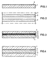
- Fig. 1 shows a conductor arrangement in a side view.
- a transparent, conductive layer 2 is applied on a carrier material 1, in the present case glass.
- This transparent, conductive layer can be a metal layer, such as B. of tin, zinc, silver, titanium, iron, Chrome, cobalt or aluminum, the layer can but also consist of a metal oxide layer, such as. B. ITO (indium tin oxide), or from cadmium tin oxide. In the present case, it is an ITO layer.
- This layer 2 is carried out in a known manner Steaming, spraying, vaporizing or sputtering on the Carrier material applied.
- the ITO layer used here has a specific resistance ⁇ sch of 0.007 Ohm.mm.
- the layer thickness d sch to be applied is 350 nm.
- the width b sch is 50 mm and the length l sch of the transparent, conductive layer is 400 mm.
- R total 320 ohms.
- Fig. 2 shows the conductor arrangement of Fig. 1 with the carrier material 1 made of glass and the transparent, conductive Layers 2 in a top view. So that a circuit for a consumer through such a conductor arrangement are formed, for example a Voltage source at one end of the conductor arrangement is attached and a consumer at the other end between the two transparent, conductive layers is appropriate.
- the one transparent, conductive layer can then serve as a forward line and the other as a return line be considered.
- FIG. 3 shows an alternative embodiment in a side view the conductor arrangement.
- a transparent, conductive layer 2 attached and on this layer 2 a so-called insulation layer 3 is applied.
- this insulation layer 3 can be transparent and vapor-deposited become. To increase performance, you can interact several transparent, conductive layers and insulation layers be arranged one above the other.
- Fig. 4 shows a further embodiment of the conductor arrangement.
- the conductor arrangement consists of a composite arrangement, whereby between two carrier materials 1 in each case a transparent layer 2 is arranged.
- This Execution possibility has the advantage of a special high stability.
- FIG. 5 shows a side view of an electrical device, in this case a lighting device 4, with the conductor arrangement according to the invention.
- the lighting device 4 is on a cable feed 5 known way with a voltage source, not shown connected.
- the cable feed 5 ends in the base element 6, on which the conductor arrangement is pivotally arranged is.
- the conductor arrangement consists of two carrier materials 1 on which transparent, conductive layers 2 are applied facing each other.
- the carrier materials 1 with the transparent, conductive layers 2 are slidable to each other, creating a power control is possible.
- a consumer 7 On the one facing away from the base element 6 End of the conductor arrangement is a consumer 7, in in this case an incandescent lamp. This consumer too can be slidably arranged on the conductor arrangement to enable performance control.
Landscapes
- Engineering & Computer Science (AREA)
- Microelectronics & Electronic Packaging (AREA)
- Surface Treatment Of Glass (AREA)
- Circuit Arrangement For Electric Light Sources In General (AREA)
- Arrangement Of Elements, Cooling, Sealing, Or The Like Of Lighting Devices (AREA)
- Non-Insulated Conductors (AREA)
- Insulated Conductors (AREA)
- Resistance Heating (AREA)
- Circuit Arrangements For Discharge Lamps (AREA)
- Laminated Bodies (AREA)
- Non-Portable Lighting Devices Or Systems Thereof (AREA)
Claims (10)
- Dispositif électrique (4) comportant un raccordement électrique et un aménagement conducteur constitué d'un matériau support (1) non conducteur avec au moins une couche (2) transparente conductrice de l'électricité,
caractérisé par le fait qu'au moins un dispositif (7) à alimenter avec du courant est relié par l'aménagement conducteur au raccordement électrique, et que la couche (2) transparente conductrice de l'électricité, ayant une superficie de section de couche Asch et une résistivité δsch , présente un rapport δsch/Asch ≤ 0,4 Ohm/mm, de préférence ≤ 0,3 Ohm/mm. - Dispositif selon la revendication 1, caractérisé par le fait que le dispositif à alimenter en courant se compose d'une lampe (7).
- Dispositif selon la revendication 1 ou 2, caractérisé par le fait que le matériau support (1) est du verre.
- Dispositif selon l'une des revendications 1 à 3, caractérisé par le fait que la couche (2) transparente conductrice est une couche de métal ou d'oxyde métallique.
- Dispositif selon l'une des revendications 1 à 4, caractérisé par le fait que la couche (2) transparente conductrice présente une épaisseur de couche de 350 nm.
- Dispositif selon l'une des revendications 1 à 5, caractérisé par le fait que plusieurs couches (2) transparentes conductrices, séparées respectivement l'une de l'autre par une couche d'isolation (3) transparente, sont disposées sur le matériau support (1) non conducteur.
- Dispositif selon l'une des revendications 1 à 6, caractérisé par le fait que plusieurs matériaux supports (1) non conducteurs avec leurs couches (2) transparentes conductrices sont disposés l'un sur l'autre.
- Dispositif selon la revendication 7, caractérisé par le fait que les matériaux supports (1) sont disposés de manière coulissante l'un par rapport à l'autre.
- Dispositif selon la revendication 7 ou 8, caractérisé par le fait que les couches (2) transparentes conductrices sont disposées tournées l'une vers l'autre sur les matériaux supports et se trouvent en contact l'une avec l'autre.
- Dispositif selon l'une des revendications 1 à 9, caractérisé par le fait que le dispositif (7) recevant le courant est monté coulissant sur l'aménagement conducteur (1, 2).
Applications Claiming Priority (4)
| Application Number | Priority Date | Filing Date | Title |
|---|---|---|---|
| DE29711973U | 1997-07-08 | ||
| DE29711973U DE29711973U1 (de) | 1997-07-08 | 1997-07-08 | Elektrische Vorrichtung, elektrisches Gerät bzw. Beleuchtungsvorrichtung |
| PCT/EP1998/003894 WO1999003111A1 (fr) | 1997-07-08 | 1998-06-25 | Dispositif electrique, appareil electrique et dispositif d'eclairage |
| CA002266713A CA2266713C (fr) | 1997-07-08 | 1999-03-23 | Dispositif d'alimentation d'appareil d'eclairage |
Publications (2)
| Publication Number | Publication Date |
|---|---|
| EP0995199A1 EP0995199A1 (fr) | 2000-04-26 |
| EP0995199B1 true EP0995199B1 (fr) | 2002-08-21 |
Family
ID=32094346
Family Applications (1)
| Application Number | Title | Priority Date | Filing Date |
|---|---|---|---|
| EP98937547A Revoked EP0995199B1 (fr) | 1997-07-08 | 1998-06-25 | Dispositif electrique, appareil electrique et dispositif d'eclairage |
Country Status (9)
| Country | Link |
|---|---|
| US (1) | US6323429B1 (fr) |
| EP (1) | EP0995199B1 (fr) |
| JP (1) | JP4497718B2 (fr) |
| AT (1) | ATE222663T1 (fr) |
| CA (1) | CA2266713C (fr) |
| DE (2) | DE29711973U1 (fr) |
| DK (1) | DK0995199T3 (fr) |
| ES (1) | ES2182352T3 (fr) |
| WO (1) | WO1999003111A1 (fr) |
Cited By (4)
| Publication number | Priority date | Publication date | Assignee | Title |
|---|---|---|---|---|
| US6865848B2 (en) | 2002-03-12 | 2005-03-15 | Maria Krimmel | Sliding element system which includes a single support rod defining two mutually insulated electrically conductive paths |
| JP2008275922A (ja) * | 2007-04-27 | 2008-11-13 | Fujikura Ltd | 表示装置 |
| JP2008275916A (ja) * | 2007-04-27 | 2008-11-13 | Fujikura Ltd | 表示装置 |
| JP2008275921A (ja) * | 2007-04-27 | 2008-11-13 | Fujikura Ltd | 表示装置 |
Families Citing this family (12)
| Publication number | Priority date | Publication date | Assignee | Title |
|---|---|---|---|---|
| DE19944170A1 (de) * | 1999-09-15 | 2001-03-22 | Merten Gmbh & Co Kg | Elektrische Vorrichtung und Verfahren zu ihrer Herstellung |
| ATE278862T1 (de) | 2001-02-05 | 2004-10-15 | Schott Spezialglas Gmbh | Glastür mit in das glas integrierter elektrischer einrichtung |
| DE10122370C2 (de) * | 2001-05-09 | 2003-06-12 | Sws Glasbaubeschlaege Gmbh | Punkthalter |
| DE10124086B4 (de) * | 2001-05-16 | 2013-11-07 | Schott Ag | Elektrisches Gerät mit einer transparenten Stromzuführung |
| DE10132963C1 (de) * | 2001-07-06 | 2002-11-14 | Sws Glasbaubeschlaege Gmbh | Klemmvorrichtung zum Befestigen von Platten, insbesondere Glasscheiben |
| DE20208703U1 (de) | 2002-06-05 | 2002-09-12 | SWS Gesellschaft für Glasbaubeschläge mbH, 51545 Waldbröl | Vorrichtung zum Anschließen von mehrschichtigen Glasscheiben mit mindestens einer elektrisch leitenden Schicht an eine elektrische Spannungsquelle |
| DE10224985B3 (de) | 2002-06-05 | 2004-01-22 | Dietrich Menzel | Träger mit einem Kabelkanal für eine Elektroleuchte und Verfahren zu seiner Herstellung |
| DE10247553B4 (de) * | 2002-10-11 | 2005-09-15 | Frerichs Glas Gmbh | Optische Anzeigeeinrichtung |
| BE1015302A3 (fr) * | 2003-01-10 | 2005-01-11 | Glaverbel | Vitrage comportant des composants electroniques. |
| GB0600215D0 (en) | 2006-01-06 | 2006-02-15 | Pilkington Automotive D Gmbh | Vehicle glazing |
| EP2009615A4 (fr) * | 2006-04-20 | 2013-04-03 | Fujikura Ltd | Dispositif d'affichage et son procede de fabrication, procede d'affichage de motifs, et dispositif d'obturation et procede associe |
| ITAN20130127A1 (it) * | 2012-08-03 | 2014-02-04 | M D Srl | Lampada con schede di circuito stampato. |
Family Cites Families (27)
| Publication number | Priority date | Publication date | Assignee | Title |
|---|---|---|---|---|
| FR1580868A (fr) * | 1968-02-21 | 1969-09-12 | ||
| US3576941A (en) * | 1969-08-06 | 1971-05-04 | Ibm | Flat power-distribution cable |
| US3586757A (en) * | 1969-08-14 | 1971-06-22 | Merle Haldeman Jr | Flexible stripline transmission line |
| US3805213A (en) * | 1972-03-22 | 1974-04-16 | Data General Corp | Flexible circuit connectors |
| DE3446662A1 (de) * | 1984-12-18 | 1986-06-26 | Werner 1000 Berlin Krbalek | Jalousie |
| JPH0411288Y2 (fr) * | 1985-04-24 | 1992-03-19 | ||
| JPH0731950B2 (ja) * | 1985-11-22 | 1995-04-10 | 株式会社リコー | 透明導電膜の製造方法 |
| JPS63184210A (ja) * | 1987-01-27 | 1988-07-29 | 日本板硝子株式会社 | 透明導電体の製造方法 |
| JPS63212983A (ja) * | 1987-02-27 | 1988-09-05 | 積水化学工業株式会社 | 看板 |
| JPS63294591A (ja) * | 1987-05-27 | 1988-12-01 | 積水化学工業株式会社 | 表示装置 |
| DE3903202C2 (de) * | 1988-02-03 | 2000-06-21 | Peter Guss | Elektrische Leuchte |
| JP2849388B2 (ja) * | 1988-06-10 | 1999-01-20 | 三井化学株式会社 | 積層導電膜 |
| JPH0817109B2 (ja) * | 1989-08-18 | 1996-02-21 | 株式会社半導体エネルギー研究所 | 電気配線およびその接続方法 |
| JPH03266884A (ja) * | 1990-03-16 | 1991-11-27 | Sekisui Chem Co Ltd | 表示装置 |
| JPH05178644A (ja) * | 1991-06-26 | 1993-07-20 | Sekisui Chem Co Ltd | 合わせガラス用中間膜及び合わせガラス |
| JPH0521120A (ja) * | 1991-07-16 | 1993-01-29 | Sekisui Chem Co Ltd | 電気装置 |
| DE4124684A1 (de) * | 1991-07-25 | 1993-01-28 | Bauerhin I G Elektro Tech | Flaechenheizelement und verfahren zu seiner herstellung |
| DE4134836A1 (de) * | 1991-10-22 | 1993-04-29 | Ewald Winkelbauer | Leuchte |
| JP3338085B2 (ja) * | 1992-08-12 | 2002-10-28 | シャープ株式会社 | 透明導電膜 |
| JPH0638115U (ja) * | 1992-10-28 | 1994-05-20 | 日本板硝子株式会社 | 照明装置の通電構造 |
| DE9215662U1 (de) * | 1992-11-17 | 1993-01-21 | GHM Ges. mbH Schöninger, 92706 Luhe-Wildenau | Spiegel mit Leuchte |
| JPH07173610A (ja) * | 1993-08-02 | 1995-07-11 | Agency Of Ind Science & Technol | 透明導電性超薄膜及びその製造方法 |
| US5413659A (en) * | 1993-09-30 | 1995-05-09 | Minnesota Mining And Manufacturing Company | Array of conductive pathways |
| US5407602A (en) * | 1993-10-27 | 1995-04-18 | At&T Corp. | Transparent conductors comprising gallium-indium-oxide |
| DE4337986C2 (de) * | 1993-11-06 | 1996-06-05 | Schott Glaswerke | Verwendungen von Sn(IV)-Carboxylaten als Ausgangsverbindungen für Tauchlösungen zur Herstellung transparenter, elektrisch leitfähiger Einkomponentenschichten aus reinem oder dotiertem SnO¶2¶ auf Glassubstraten |
| EP0707320A1 (fr) * | 1994-10-13 | 1996-04-17 | AT&T Corp. | Conducteurs transparents comprenant de l'oxyde de zinc et d'indium et méthodes de fabrication de films |
| US5607789A (en) * | 1995-01-23 | 1997-03-04 | Duracell Inc. | Light transparent multilayer moisture barrier for electrochemical cell tester and cell employing same |
-
1997
- 1997-07-08 DE DE29711973U patent/DE29711973U1/de not_active Expired - Lifetime
-
1998
- 1998-06-25 EP EP98937547A patent/EP0995199B1/fr not_active Revoked
- 1998-06-25 AT AT98937547T patent/ATE222663T1/de not_active IP Right Cessation
- 1998-06-25 WO PCT/EP1998/003894 patent/WO1999003111A1/fr not_active Ceased
- 1998-06-25 US US09/462,158 patent/US6323429B1/en not_active Expired - Fee Related
- 1998-06-25 JP JP2000502510A patent/JP4497718B2/ja not_active Expired - Lifetime
- 1998-06-25 DE DE59805255T patent/DE59805255D1/de not_active Revoked
- 1998-06-25 ES ES98937547T patent/ES2182352T3/es not_active Expired - Lifetime
- 1998-06-25 DK DK98937547T patent/DK0995199T3/da active
-
1999
- 1999-03-23 CA CA002266713A patent/CA2266713C/fr not_active Expired - Fee Related
Cited By (4)
| Publication number | Priority date | Publication date | Assignee | Title |
|---|---|---|---|---|
| US6865848B2 (en) | 2002-03-12 | 2005-03-15 | Maria Krimmel | Sliding element system which includes a single support rod defining two mutually insulated electrically conductive paths |
| JP2008275922A (ja) * | 2007-04-27 | 2008-11-13 | Fujikura Ltd | 表示装置 |
| JP2008275916A (ja) * | 2007-04-27 | 2008-11-13 | Fujikura Ltd | 表示装置 |
| JP2008275921A (ja) * | 2007-04-27 | 2008-11-13 | Fujikura Ltd | 表示装置 |
Also Published As
| Publication number | Publication date |
|---|---|
| ATE222663T1 (de) | 2002-09-15 |
| ES2182352T3 (es) | 2003-03-01 |
| JP4497718B2 (ja) | 2010-07-07 |
| CA2266713A1 (fr) | 2000-09-23 |
| WO1999003111A1 (fr) | 1999-01-21 |
| EP0995199A1 (fr) | 2000-04-26 |
| DE59805255D1 (de) | 2002-09-26 |
| JP2002528847A (ja) | 2002-09-03 |
| US6323429B1 (en) | 2001-11-27 |
| CA2266713C (fr) | 2005-05-10 |
| DK0995199T3 (da) | 2002-12-16 |
| DE29711973U1 (de) | 1998-11-05 |
Similar Documents
| Publication | Publication Date | Title |
|---|---|---|
| EP0995199B1 (fr) | Dispositif electrique, appareil electrique et dispositif d'eclairage | |
| EP2008291B1 (fr) | Appareillage d'installation électrique | |
| EP0866639B1 (fr) | Chauffage ohmique pour les objects plats, en particulier pour miroirs | |
| EP0900971A1 (fr) | Dispositif d'éclairage avec diodes électroluminescentes montées sur une plaque en verre | |
| EP1619524A4 (fr) | Feuille de diffusion de lumiere a blindage electromagnetique | |
| DE10326684A1 (de) | Sensorvorrichtung | |
| DE3903202C2 (de) | Elektrische Leuchte | |
| EP0825666A3 (fr) | Antenne de vitre avec une couche transparente conductive | |
| WO2004084683A1 (fr) | Miroir | |
| WO2009003652A1 (fr) | Substrat comprenant une couche hautement conductrice | |
| DE102004029164B4 (de) | Verbundglasscheibe mit segmentierter Leitschicht und Sammelschienenanordnung dafür | |
| DE4338221A1 (de) | Spiegel mit Leuchte | |
| WO1982003723A1 (fr) | Contact electrique, notamment pour circuits imprimes de petits appareils electriques | |
| EP1799019B1 (fr) | Raccordement électrique pour un socle | |
| EP1470745B1 (fr) | Boitier pour appareils de l'electronique de divertissement | |
| DE1958496A1 (de) | Fenster aus gehaertetem Glas | |
| EP2622986B1 (fr) | Lisseur capillaire électrique | |
| DE102018107309B4 (de) | Transparente Anzeigevorrichtung | |
| EP0557753B1 (fr) | Dispositif de protection d'un appareil | |
| DE10012264A1 (de) | Schalttafel | |
| EP1215649A2 (fr) | Panneau d'affichage au plasma | |
| DE2641105A1 (de) | Dimmer mit bistabilem speicher und beruehrungssensor fuer leuchten | |
| EP0626715A2 (fr) | Lampe luminescente pour insertion | |
| DE19651800A1 (de) | Leitungs-Steckverbindung | |
| DE102016002074B4 (de) | System mit erstem Elektrogerät und Kabel zur Verbindung mit einem weiteren Elektrogerät |
Legal Events
| Date | Code | Title | Description |
|---|---|---|---|
| PUAI | Public reference made under article 153(3) epc to a published international application that has entered the european phase |
Free format text: ORIGINAL CODE: 0009012 |
|
| 17P | Request for examination filed |
Effective date: 20000110 |
|
| AK | Designated contracting states |
Kind code of ref document: A1 Designated state(s): AT CH DE DK ES FI FR GB IT LI LU NL PT SE |
|
| AX | Request for extension of the european patent |
Free format text: LT PAYMENT 20000110;LV PAYMENT 20000110 |
|
| GRAG | Despatch of communication of intention to grant |
Free format text: ORIGINAL CODE: EPIDOS AGRA |
|
| GRAG | Despatch of communication of intention to grant |
Free format text: ORIGINAL CODE: EPIDOS AGRA |
|
| GRAG | Despatch of communication of intention to grant |
Free format text: ORIGINAL CODE: EPIDOS AGRA |
|
| GRAH | Despatch of communication of intention to grant a patent |
Free format text: ORIGINAL CODE: EPIDOS IGRA |
|
| 17Q | First examination report despatched |
Effective date: 20020411 |
|
| GRAH | Despatch of communication of intention to grant a patent |
Free format text: ORIGINAL CODE: EPIDOS IGRA |
|
| GRAA | (expected) grant |
Free format text: ORIGINAL CODE: 0009210 |
|
| AK | Designated contracting states |
Kind code of ref document: B1 Designated state(s): AT CH DE DK ES FI FR GB IT LI LU NL PT SE |
|
| AX | Request for extension of the european patent |
Free format text: LT PAYMENT 20000110;LV PAYMENT 20000110 |
|
| PG25 | Lapsed in a contracting state [announced via postgrant information from national office to epo] |
Ref country code: FI Free format text: LAPSE BECAUSE OF FAILURE TO SUBMIT A TRANSLATION OF THE DESCRIPTION OR TO PAY THE FEE WITHIN THE PRESCRIBED TIME-LIMIT Effective date: 20020821 |
|
| REF | Corresponds to: |
Ref document number: 222663 Country of ref document: AT Date of ref document: 20020915 Kind code of ref document: T |
|
| REG | Reference to a national code |
Ref country code: GB Ref legal event code: FG4D Free format text: NOT ENGLISH |
|
| REG | Reference to a national code |
Ref country code: CH Ref legal event code: EP |
|
| REF | Corresponds to: |
Ref document number: 59805255 Country of ref document: DE Date of ref document: 20020926 |
|
| REG | Reference to a national code |
Ref country code: CH Ref legal event code: NV Representative=s name: TROESCH SCHEIDEGGER WERNER AG |
|
| PG25 | Lapsed in a contracting state [announced via postgrant information from national office to epo] |
Ref country code: PT Free format text: LAPSE BECAUSE OF FAILURE TO SUBMIT A TRANSLATION OF THE DESCRIPTION OR TO PAY THE FEE WITHIN THE PRESCRIBED TIME-LIMIT Effective date: 20021205 |
|
| GBT | Gb: translation of ep patent filed (gb section 77(6)(a)/1977) |
Effective date: 20021119 |
|
| REG | Reference to a national code |
Ref country code: DK Ref legal event code: T3 |
|
| LTIE | Lt: invalidation of european patent or patent extension |
Effective date: 20020821 |
|
| ET | Fr: translation filed | ||
| REG | Reference to a national code |
Ref country code: ES Ref legal event code: FG2A Ref document number: 2182352 Country of ref document: ES Kind code of ref document: T3 |
|
| PLBQ | Unpublished change to opponent data |
Free format text: ORIGINAL CODE: EPIDOS OPPO |
|
| PLBQ | Unpublished change to opponent data |
Free format text: ORIGINAL CODE: EPIDOS OPPO |
|
| PLBI | Opposition filed |
Free format text: ORIGINAL CODE: 0009260 |
|
| PLBQ | Unpublished change to opponent data |
Free format text: ORIGINAL CODE: EPIDOS OPPO |
|
| PLBQ | Unpublished change to opponent data |
Free format text: ORIGINAL CODE: EPIDOS OPPO |
|
| PLBI | Opposition filed |
Free format text: ORIGINAL CODE: 0009260 |
|
| PG25 | Lapsed in a contracting state [announced via postgrant information from national office to epo] |
Ref country code: LU Free format text: LAPSE BECAUSE OF NON-PAYMENT OF DUE FEES Effective date: 20030625 |
|
| PLAX | Notice of opposition and request to file observation + time limit sent |
Free format text: ORIGINAL CODE: EPIDOSNOBS2 |
|
| 26 | Opposition filed |
Opponent name: SCHOTT GLAS / SCHOTT SPEZIALGLAS GMBH Effective date: 20030516 |
|
| 26 | Opposition filed |
Opponent name: JAEGER, STEFFEN, DR. Effective date: 20030521 Opponent name: HARTMANN, RAINER, DR. Effective date: 20030521 Opponent name: SCHOTT GLAS / SCHOTT SPEZIALGLAS GMBH Effective date: 20030516 |
|
| NLR1 | Nl: opposition has been filed with the epo |
Opponent name: JAEGER, STEFFEN, DR. Opponent name: HARTMANN, RAINER, DR. Opponent name: SCHOTT GLAS / SCHOTT SPEZIALGLAS GMBH |
|
| PLBB | Reply of patent proprietor to notice(s) of opposition received |
Free format text: ORIGINAL CODE: EPIDOSNOBS3 |
|
| PLAB | Opposition data, opponent's data or that of the opponent's representative modified |
Free format text: ORIGINAL CODE: 0009299OPPO |
|
| PLAQ | Examination of admissibility of opposition: information related to despatch of communication + time limit deleted |
Free format text: ORIGINAL CODE: EPIDOSDOPE2 |
|
| PLAR | Examination of admissibility of opposition: information related to receipt of reply deleted |
Free format text: ORIGINAL CODE: EPIDOSDOPE4 |
|
| PLBQ | Unpublished change to opponent data |
Free format text: ORIGINAL CODE: EPIDOS OPPO |
|
| R26 | Opposition filed (corrected) |
Opponent name: JAEGER, STEFFEN, DR. Effective date: 20030521 Opponent name: HARTMANN, RAINER, DR. Effective date: 20030521 Opponent name: SCHOTT GLAS / SCHOTT SPEZIALGLAS GMBH Effective date: 20030516 |
|
| PLAQ | Examination of admissibility of opposition: information related to despatch of communication + time limit deleted |
Free format text: ORIGINAL CODE: EPIDOSDOPE2 |
|
| PLAR | Examination of admissibility of opposition: information related to receipt of reply deleted |
Free format text: ORIGINAL CODE: EPIDOSDOPE4 |
|
| PLBQ | Unpublished change to opponent data |
Free format text: ORIGINAL CODE: EPIDOS OPPO |
|
| PLAB | Opposition data, opponent's data or that of the opponent's representative modified |
Free format text: ORIGINAL CODE: 0009299OPPO |
|
| NLR1 | Nl: opposition has been filed with the epo |
Opponent name: JAEGER, STEFFEN, DR. Opponent name: HARTMANN, RAINER, DR. Opponent name: SCHOTT GLAS / SCHOTT SPEZIALGLAS GMBH |
|
| R26 | Opposition filed (corrected) |
Opponent name: JAEGER, STEFFEN, DR. Effective date: 20030521 Opponent name: HARTMANN, RAINER, DR. Effective date: 20030521 Opponent name: SCHOTT AG Effective date: 20030516 |
|
| NLR1 | Nl: opposition has been filed with the epo |
Opponent name: JAEGER, STEFFEN, DR. Opponent name: HARTMANN, RAINER, DR. Opponent name: SCHOTT AG |
|
| PLCK | Communication despatched that opposition was rejected |
Free format text: ORIGINAL CODE: EPIDOSNREJ1 |
|
| APBP | Date of receipt of notice of appeal recorded |
Free format text: ORIGINAL CODE: EPIDOSNNOA2O |
|
| APAH | Appeal reference modified |
Free format text: ORIGINAL CODE: EPIDOSCREFNO |
|
| APBP | Date of receipt of notice of appeal recorded |
Free format text: ORIGINAL CODE: EPIDOSNNOA2O |
|
| APBQ | Date of receipt of statement of grounds of appeal recorded |
Free format text: ORIGINAL CODE: EPIDOSNNOA3O |
|
| APAL | Date of receipt of statement of grounds of an appeal modified |
Free format text: ORIGINAL CODE: EPIDOSCNOA3O |
|
| APBQ | Date of receipt of statement of grounds of appeal recorded |
Free format text: ORIGINAL CODE: EPIDOSNNOA3O |
|
| PGFP | Annual fee paid to national office [announced via postgrant information from national office to epo] |
Ref country code: DE Payment date: 20080819 Year of fee payment: 11 |
|
| APBU | Appeal procedure closed |
Free format text: ORIGINAL CODE: EPIDOSNNOA9O |
|
| PGFP | Annual fee paid to national office [announced via postgrant information from national office to epo] |
Ref country code: NL Payment date: 20090624 Year of fee payment: 12 Ref country code: ES Payment date: 20090629 Year of fee payment: 12 Ref country code: DK Payment date: 20090622 Year of fee payment: 12 |
|
| PGFP | Annual fee paid to national office [announced via postgrant information from national office to epo] |
Ref country code: SE Payment date: 20090623 Year of fee payment: 12 Ref country code: AT Payment date: 20090622 Year of fee payment: 12 |
|
| POAG | Date of filing of petition for review recorded |
Free format text: ORIGINAL CODE: EPIDOSNPRV3 |
|
| POAH | Number of petition for review recorded |
Free format text: ORIGINAL CODE: EPIDOSNPRV1 |
|
| POAI | Petitioner in petition for review recorded |
Free format text: ORIGINAL CODE: EPIDOSNPRV2 |
|
| RDAF | Communication despatched that patent is revoked |
Free format text: ORIGINAL CODE: EPIDOSNREV1 |
|
| RDAG | Patent revoked |
Free format text: ORIGINAL CODE: 0009271 |
|
| STAA | Information on the status of an ep patent application or granted ep patent |
Free format text: STATUS: PATENT REVOKED |
|
| REG | Reference to a national code |
Ref country code: CH Ref legal event code: PL |
|
| 27W | Patent revoked |
Effective date: 20090507 |
|
| GBPR | Gb: patent revoked under art. 102 of the ep convention designating the uk as contracting state |
Effective date: 20090507 |
|
| PG25 | Lapsed in a contracting state [announced via postgrant information from national office to epo] |
Ref country code: LI Free format text: LAPSE BECAUSE OF THE APPLICANT RENOUNCES Effective date: 20020821 Ref country code: CH Free format text: LAPSE BECAUSE OF THE APPLICANT RENOUNCES Effective date: 20020821 |
|
| PGFP | Annual fee paid to national office [announced via postgrant information from national office to epo] |
Ref country code: FR Payment date: 20090618 Year of fee payment: 12 Ref country code: CH Payment date: 20090624 Year of fee payment: 12 |
|
| PGFP | Annual fee paid to national office [announced via postgrant information from national office to epo] |
Ref country code: GB Payment date: 20090623 Year of fee payment: 12 |
|
| NLR2 | Nl: decision of opposition |
Effective date: 20090507 |
|
| REG | Reference to a national code |
Ref country code: SE Ref legal event code: ECNC |
|
| PGFP | Annual fee paid to national office [announced via postgrant information from national office to epo] |
Ref country code: IT Payment date: 20090627 Year of fee payment: 12 |
|
| POAK | Decision taken: petition for review obviously unsubstantiated |
Free format text: ORIGINAL CODE: 0009255 |
|
| PRVN | Petition for review not allowed |
Free format text: REJECTION OF THE PETITION FOR REVIEW Effective date: 20100705 |