EP0996263B1 - Schaltung zur Rechnung der Steuerung einer Signalpunktordnung - Google Patents
Schaltung zur Rechnung der Steuerung einer Signalpunktordnung Download PDFInfo
- Publication number
- EP0996263B1 EP0996263B1 EP98921725A EP98921725A EP0996263B1 EP 0996263 B1 EP0996263 B1 EP 0996263B1 EP 98921725 A EP98921725 A EP 98921725A EP 98921725 A EP98921725 A EP 98921725A EP 0996263 B1 EP0996263 B1 EP 0996263B1
- Authority
- EP
- European Patent Office
- Prior art keywords
- signal
- baseband signal
- point arrangement
- signal point
- circuit
- Prior art date
- Legal status (The legal status is an assumption and is not a legal conclusion. Google has not performed a legal analysis and makes no representation as to the accuracy of the status listed.)
- Expired - Lifetime
Links
- 239000006185 dispersion Substances 0.000 title claims description 44
- 238000006243 chemical reaction Methods 0.000 claims description 42
- 238000010586 diagram Methods 0.000 description 6
- 238000000653 depth-selective Mossbauer spectroscopy Methods 0.000 description 4
- 230000005540 biological transmission Effects 0.000 description 2
- 238000007796 conventional method Methods 0.000 description 1
- 238000000034 method Methods 0.000 description 1
- 230000010363 phase shift Effects 0.000 description 1
Images


Classifications
-
- H—ELECTRICITY
- H04—ELECTRIC COMMUNICATION TECHNIQUE
- H04L—TRANSMISSION OF DIGITAL INFORMATION, e.g. TELEGRAPHIC COMMUNICATION
- H04L27/00—Modulated-carrier systems
- H04L27/18—Phase-modulated carrier systems, i.e. using phase-shift keying
- H04L27/22—Demodulator circuits; Receiver circuits
Definitions
- the present invention relates to a signal point arrangement dispersion value calculation circuit for calculating a signal point arrangement dispersion value of a baseband signal demodulated from a received phase shift keying signal, and more particularly to a signal point arrangement dispersion value calculation circuit used with a carrier reproduction circuit for reproducing a carrier from a demodulated baseband signal or an absolute phasing circuit for making the phase angle of a baseband signal demodulated from a reception signal point arrangement coincide with a transmission signal phase angle.
- a known broadcasting receiver for receiving digitally modulated radio waves such as 8PSK modulated waves, QPSK modulated waves and BPSK modulated waves controls the frequency of a reproduction carrier wave in accordance with a signal point dispersion value of a baseband signal.
- arrangement of a demodulated baseband signal, and in accordance with the obtained reception signal phase rotation angle, the phase of the demodulated baseband signal is rotated reversely to execute absolute phasing, i.e, to make the demodulation baseband signal coincide with the transmission signal phase angle.
- the demodulated baseband signals (I, Q) have reference positions (0, 0), (0, 1), (1, 1) and (1, 0) in which (0, 0) is set in the first quadrant, (0, 1) is set in the second quadrant, (1, 1) is set in the third quadrant and (1, 0) is set in the fourth quadrant, and (0, 1) is rotated by 90° in the clockwise direction, (1, 1) is rotated by 180° in the clockwise direction and (1, 0) is rotated by 90° in the counter-clockwise direction to set all reference positions in the first quadrant.
- the demodulated baseband signals (I, Q) set in the first quadrant are supplied to a signal point arrangement conversion circuit to convert the signals into signal point arrangement conversion data.
- Dispersion values are calculated from the signal point arrangement conversion data converted by the signal point arrangement conversion circuit, and compared with a predetermined reference value A to count the occurrence frequency of dispersion values equal to or larger than the reference value A during a predetermined unit period.
- a total sum DSMS of occurrence frequencies of dispersion values equal to or larger than the reference value A during the predetermined unit period is calculated.
- a C/N is judged and in accordance with the judged C/N, the frequency of a reproduction carrier is controlled.
- the signal point arrangement conversion circuit operates to set the baseband signals (I, Q) to the first quadrant.
- setting the baseband signals to the first quadrant is realized by exchanging the I axis or Q axis in each quadrant.
- baseband signals are set to the first quadrant by using a conversion table stored in a ROM.
- the signal point arrangement conversion is performed by using a conversion table stored in ROM, the size of the conversion table stored in ROM becomes too large to be implemented in an integrated circuit.
- the invention is as follows:
- a signal point arrangement dispersion calculation circuit of this invention comprises: a phase rotation circuit for rotating a phase of a demodulated baseband signal; a signal point arrangement conversion circuit for judging a signal point arrangement of the demodulated baseband signal in accordance with the demodulated baseband signal and a baseband signal whose phase is rotated by the phase rotation circuit, and in accordance with the judged signal point arrangement, converting the signal point arrangement of the demodulated baseband signal into a predetermined quadrant by using the demodulated baseband signal and the baseband signal whose phase is rotated by the phase rotation circuit; and dispersion value calculating means for calculating a dispersion value in accordance with the baseband signal whose signal point arrangement is converted.
- a signal point arrangement dispersion calculation circuit of this invention comprises: a phase rotation circuit for rotating a phase of a demodulated baseband signal by 22.5° at a speed twice as fast as a symbol rate of the demodulated baseband signal; a signal point arrangement conversion circuit for judging a signal point arrangement of the demodulated baseband signal in accordance with the demodulated baseband signal and a baseband signal whose phase is rotated by the phase rotation circuit, and in accordance with the judged signal point arrangement, converting the signal point arrangement of the demodulated baseband signal into a predetermined quadrant by using the demodulated baseband signal and the baseband signal whose phase is rotated by 45° through consecutive two rotations by the phase rotation circuit; and dispersion value calculating means for calculating a dispersion value in accordance with the baseband signal whose signal point arrangement is converted.
- the phase rotation circuit rotates rotating the phase of a demodulated baseband signal by 22.5° at a speed twice as fast as a symbol rate of the demodulated baseband signal.
- the signal point arrangement conversion circuit judges a signal point arrangement of the demodulated baseband signal in accordance with the demodulated baseband signal and a baseband signal whose phase is rotated by the phase rotation circuit, and in accordance with the judged signal point arrangement, converts the signal point arrangement of the demodulated baseband signal into a predetermined quadrant by using the demodulated baseband signal and the baseband signal whose phase is rotated by 45° through consecutive two rotations by the phase rotation circuit; and the dispersion value calculating means calculates a dispersion value in accordance with the baseband signal whose signal point arrangement is converted.
- the signal point arrangement of the demodulated baseband signal is judged in accordance with the demodulated baseband signal and a baseband signal whose phase is rotated by 22.5° by the phase rotation circuit, and in accordance with the judged signal point arrangement, the signal point arrangement of the demodulated baseband signal is converted by using the demodulated baseband signal and the baseband signal whose phase is rotated by 45 through consecutive two rotations by the phase rotation circuit. Accordingly, a conventional conversion table stored in ROM for signal point arrangement conversion is not necessary, and the signal point arrangement conversion circuit can be realized by logic circuits to thus reduce the circuit scale.
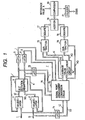
- FIG. 1 is a block diagram showing the structure of the signal point arrangement dispersion value calculation circuit of the embodiment.
- Baseband signals (I, Q) demodulated by an unrepresented demodulation circuit are supplied to select/latch circuits 1 and 2.
- Latch outputs (SI, SQ) of the select/latch circuits 1 and 2 are supplied to a 22.5° turning remapper 3 to rotate the coordinate system by 22.5° in the counter-clockwise direction.
- Baseband output signals (i', q') of the 22.5° turning remapper 3 are supplied to the select/latch circuits 1 and 2.
- the select/latch circuits 1 and 2 alternately latch the input baseband signals (I, Q) and (i', q') at a half period of a symbol rate period synchronizing with the symbol rate.
- the 22.5° turning remapper 3 can therefore be structured by coefficient multiplication circuits and addition/subtraction circuits.
- the output baseband signals (i', q') of the 22.5° turning remapper 3 are supplied to latch circuits 5 and 6 which latch them at the symbol rate period. Therefore, the latch circuits 5 and 6 output baseband signals (i, q) subjected to coordinate system conversion by 45°.
- the demodulated baseband signals (I, Q), baseband signals (i', q') output from the 22.5° turning remapper 3 and baseband signals (i, q) output from the latch circuits 5 and 6 are supplied to a signal point arrangement conversion - dispersion value calculation circuit 7 which executes a signal point arrangement conversion operation and a dispersion value calculation operation.
- the signal point arrangement conversion - dispersion value calculation circuit 7 includes a signal point arrangement conversion circuit 73 and an average value calculation circuit 74.
- the signal point arrangement conversion circuit 73 receives: baseband signals (LI, LQ) output from a latch circuit 71 which latches the baseband signals (I, Q) at the symbol rate period; baseband signals (li, lq) output from a latch circuit 72 which latches the baseband signals (i', q') output from the 22.5° turning remapper 3 at a half period of the symbol rate period synchronizing the symbol rate; and baseband signals (i, q) output from the latch circuit 5 and 6, and converts the signal point arrangement of the demodulated baseband signals (I, Q) into the first quadrant.
- baseband signals (LI, LQ) output from a latch circuit 71 which latches the baseband signals (I, Q) at the symbol rate period
- baseband signals (li, lq) output from a latch circuit 72 which latches the baseband signals
- the average value calculation circuit 74 calculates an average value of the baseband signals (HI, HQ) converted into the first quadrant by the signal point arrangement conversion circuit 73. Therefore, the demodulated baseband signals (I, Q) are converted to the first quadrant by the signal point arrangement conversion circuit 73, and in accordance with the baseband signals (HI, HQ) output from the signal point arrangement conversion circuit 73, the average value calculation circuit 74 calculates the average value.
- the average value calculation circuit 74 outputs baseband signals (AI, AQ).
- the signal point arrangement conversion - dispersion value calculation circuit 7 further includes: a subtraction circuit 75 for subtracting the baseband signal (AI) from the baseband signal (HI); a square circuit 77 for squaring the baseband signal output from the subtraction circuit 75; a subtraction circuit 76 for subtracting the baseband signal (AQ) from the baseband signal (HQ); a square circuit 78 for squaring the baseband signal output from the subtraction circuit 76; an adder circuit 79 for adding an output (ISQ) from the square circuit 77 and an output (QSQ) from the square circuit 78 together; a comparison circuit 80 for comparing an output (ADIQ) from the adder circuit 79 with a reference value A; and a counter 81 for counting outputs from the comparison circuit 80.
- a subtraction circuit 75 for subtracting the baseband signal (AI) from the baseband signal (HI)
- a square circuit 77 for squaring the baseband signal output from the subtraction circuit 75
- a subtraction circuit 76 for subtract
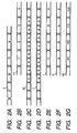
- baseband signals including: the baseband signal (I); baseband signal (LI) output from the latch circuit 71; baseband signal (SI) output from the select/latch circuit 1; baseband signal (i') output from the 22.5° turning remapper 3; baseband signal (i) output from the latch circuit 5; baseband signal (li) output from the latch circuit 72; and baseband signal (HI) output from the signal point arrangement conversion circuit 73.
- the occurrence period of the baseband signal (I) corresponds to the baseband rate.
- Symbols ia, ib, ic, ... shown in Figs. 2C and 2D schematically show the outputs from the 22.5° turning remapper 3.
- Dispersion values of the baseband signals (HI, HQ) whose signal point arrangement was converted by the signal point arrangement conversion circuit 73 are calculated by the average value calculation circuit 74, subtraction circuits 75 and 76, square circuits 77 and 78 and addition circuit 79. Dispersion values equal to or larger than the reference value A are detected by the comparison circuit 8, and a counter 81 counts the occurrence frequency of dispersion values equal to or larger than the reference value A during a predetermined unit period, to thereby obtain the total sum DSMS of occurrence frequencies of dispersion values equal to or larger than the reference value A during the unit period.
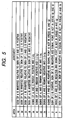
- the signal point arrangement can be judged in accordance with a change in the polarity and level of the I, Q, li, and lq axes before and after the coordinate system is rotated by the 22.5° turning remapper 3 as shown in Fig. 5 from each position in the signal arrangement.
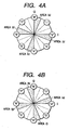
- the signal arrangement is divided as shown in Figs. 4A and 4B , into 22.5° areas including area (a), area (b), area (c), area (d), area (e), area (f), area (g) and area (h), and into ranges (represented by areas in Figs. 5 and 6 ) including range "1", range "3", range "5" and range "7".
- the signal point arrangement is judged as the area (a). If the sign of the baseband signal lq is inverted relative to the sign of the baseband signal Q and the sign of the baseband signal I is positive before and after the rotation by 22.5°, then the signal point arrangement is judged as the area (b). If the sign of the baseband signal li is inverted relative to the sign of the baseband signal I and the sign of the baseband signal Q is negative before and after the rotation by 22.5°, then the signal point arrangement is judged as the area (c). If the sign of the baseband signal lq is inverted relative to the sign of the baseband signal Q and the sign of the baseband signal I is negative before and after the rotation by 22.5°, then the signal point arrangement is judged as the area (d).
- the signal point arrangement is judged as the area (e). If the signs of the baseband signals li and I both remain positive and the baseband signals are li >
- the signal point arrangement is judged as the range "1". If the signs of the baseband signal I is positive and the sign of the baseband signal Q is negative and the signal point is neither in the area (b) nor area (f), then the signal point arrangement is judged as the range "3". If the signs of the baseband signals I and Q are negative and the signal point is neither in the area (c) nor area (g), then the signal point arrangement is judged as the range "5". If the signs of the baseband signal I is negative and the sign of the baseband signal Q is positive and the signal point is neither in the area (d) nor area (h), then the signal point arrangement is judged as the range "7".
- the baseband signal i (hereinafter described also as i axis) is converted into an absolute value thereof, the baseband signal i is replaced by the baseband signal q (hereinafter described also as q axis), and the baseband signal q is replaced by the baseband signal i, the former being output as a converted baseband signal HI and the latter being output as a converted baseband signal HQ.
- the base band signals i and q are output as converted baseband signals HI and HQ.
- the baseband signal q is converted into an absolute value thereof, the baseband signal i is replaced by the baseband signal q, and the baseband signal q is replaced by the baseband signal i, the former being output as a converted baseband signal HI and the latter being output as a converted baseband signal HQ.
- the signal point arrangement is judged as the area (d)
- the base band signals i and q are converted into the absolute values thereof, the former being output as a converted baseband signal HI and the latter being output as a converted baseband signal HQ.
- the base band signals i is output as a converted baseband signal HI, and the baseband signal q is output as a converted baseband signal HQ. If the signal point arrangement is judged as the area (f), the baseband signal q is converted into an absolute value thereof, the baseband signal i is replaced by the baseband signal q, and the baseband signal q is replaced by the baseband signal i, the former being output as a converted baseband signal HI and the latter being output as a converted baseband signal HQ.
- the base band signals i and q are converted into the absolutes thereof, the former being output as a converted baseband signal HI and the latter being output as a converted baseband signal HQ.
- the signal point arrangement is judged as the area (h)
- the baseband signal i is converted into an absolute value thereof, the baseband signal i is replaced by the baseband signal q, and the baseband signal q is replaced by the baseband signal i, the former being output as a converted baseband signal HI and the latter being output as a converted baseband signal HQ.
- the baseband signal I is output as a converted baseband signal HI and the baseband signal Q is output as a converted baseband signal HQ.
- the signal point arrangement is judged as the range (3), the baseband signal Q is converted into an absolute value thereof, the baseband signal I is replaced by the baseband signal Q, and the baseband signal Q is replaced by the baseband signal I, the former being output as a converted baseband signal HI and the latter being output as a converted baseband signal HQ.
- the signal point arrangement is judged as the range (5), the base band signals I and Q are converted into the absolutes thereof, the former being output as a converted baseband signal HI and the latter being output as a converted baseband signal HQ.
- the base band signal I is converted into the absolute value thereof, the baseband signal I is replaced by the baseband signal Q, and the baseband signal Q is replaced by the baseband signal I, the former being output as a converted baseband signal HI and the latter being output as a converted baseband signal HQ.
- the signal point arrangement conversion circuit 73 execute only a judgement based upon the rules shown in Fig. 5 and a conversion shown in Fig. 6 based upon the judgement.
- the signal point arrangement conversion circuit 73 can therefore be realized by logic circuits.
- the circuit scale can be made small, and the necessary area of this circuit in an integrated circuit can be made small.
- DSMS can be obtained through the average value calculation and dispersion value calculation in accordance with the baseband signals (HI, HQ) output from the signal point arrangement conversion circuit 73 as described earlier.
- a conversion table to be stored in a ROM for signal point arrangement conversion is not necessary for calculating signal point dispersion values.
- the circuit scale can be made small and the necessary area of this circuit in an integrated circuit can be made small.
Landscapes
- Engineering & Computer Science (AREA)
- Computer Networks & Wireless Communication (AREA)
- Signal Processing (AREA)
- Digital Transmission Methods That Use Modulated Carrier Waves (AREA)
Claims (2)
- Signalpunktanordnungs-Dispersionsberechnungsschaltung (7), welche arbeitet, um einen Dispersionswert eines Signalpunkts von einem empfangenen Signal aus 8PSKmodulierten Wellen zu berechnen, wobei die Schaltung umfasst:eine Phasendrehungsschaltung (3), welche eine Phase eines demodulierten Basisbandsignals dreht;eine Signalpunktanordnungs-Wandlungsschaltung (73), welche bestimmt, in welchem Oktanten ein Signalpunkt des demodulierten Basisbandsignals (LI, LQ) liegt, und zwar auf Grundlage des demodulierten Basisbandsignals und eines Basisbandsignals (li, lq), dessen Phase von der Phasendrehungsschaltung gedreht ist, und welche, in Übereinstimmung mit der Bestimmung, die Signalpunktanordnung des demodulierten Basisbandsignals zu einem vorbestimmten Oktanten wandelt durch Verwenden des demodulierten Basisbandsignals (LI, LQ) und des Basisbandsignals (i, q), dessen Phase von der Phasendrehungsschaltung gedreht ist; undeine Dispersionswertberechnungseinrichtung, welche einen Dispersionswert in Übereinstimmung mit dem Basisbandsignal berechnet, dessen Signalpunktanordnung gewandelt ist, wobei dieDispersionswertberechnungseinrichtung umfasst:eine Einrichtung (74), welche durchschnittliche In-Phasen-(AI)- und Quadratur-(AQ)-Werte zuvor empfangener, zum vorbestimmten Oktanten gewandelter Symbole berechnet,eine Einrichtung (75, 76), welche die In-Phasen-(HI)- und die Quadratur-(HQ)-Werte des gewandelten demodulierten Signals jeweils von den gewandelten durchschnittlichen In-Phasen-(AI)- und Quadratur-(AQ)-Werten subtrahiert,eine Einrichtung (77, 78), welche die von der Subtrahiereinrichtung (75, 76) bereitgestellte In-Phasen- und Quadratur-Differenz quadriert, undeine Einrichtung (79), welche die Summe der Quadrate als den Dispersionswert bereitstellt.
- Signalpunktanordnungs-Dispersionsberechnungsschaltung nach Anspruch 1, bei welcher
die Phasendrehungsschaltung (3) einen Rückumsetzer umfasst, welcher die Phase eines demodulierten Basisbandsignals (SI, SQ) um 22,5° mit einer Geschwindigkeit dreht, die doppelt so schnell ist wie eine Symbolrate des demodulierten Basisbandsignals; und
die Signalpunktanordnungs-Wandlungsschaltung (73) eine Schaltung umfasst, welche die Signalpunktanordnung des demodulierten Basisbandsignals (LI, LQ) zu einem vorbestimmten Oktanten wandelt durch Verwenden des demodulierten Basisbandsignals und des Basisbandsignals (i, q), dessen Phase um 45° durch zwei aufeinanderfolgende Drehungen von der Phasendrehungsschaltung gedreht wurde.
Applications Claiming Priority (3)
| Application Number | Priority Date | Filing Date | Title |
|---|---|---|---|
| JP09212745A JP3115261B2 (ja) | 1997-07-24 | 1997-07-24 | 信号点配置分散値算出回路 |
| JP21274597 | 1997-07-24 | ||
| PCT/JP1998/002204 WO1999005834A1 (fr) | 1997-07-24 | 1998-05-20 | Circuit de calcul de dispersion de la repartition des points de signal |
Publications (3)
| Publication Number | Publication Date |
|---|---|
| EP0996263A1 EP0996263A1 (de) | 2000-04-26 |
| EP0996263A4 EP0996263A4 (de) | 2005-09-07 |
| EP0996263B1 true EP0996263B1 (de) | 2009-04-22 |
Family
ID=16627731
Family Applications (1)
| Application Number | Title | Priority Date | Filing Date |
|---|---|---|---|
| EP98921725A Expired - Lifetime EP0996263B1 (de) | 1997-07-24 | 1998-05-20 | Schaltung zur Rechnung der Steuerung einer Signalpunktordnung |
Country Status (7)
| Country | Link |
|---|---|
| US (1) | US6643335B1 (de) |
| EP (1) | EP0996263B1 (de) |
| JP (1) | JP3115261B2 (de) |
| CN (1) | CN1115834C (de) |
| CA (1) | CA2296451C (de) |
| DE (1) | DE69840773D1 (de) |
| WO (1) | WO1999005834A1 (de) |
Families Citing this family (1)
| Publication number | Priority date | Publication date | Assignee | Title |
|---|---|---|---|---|
| US6697440B1 (en) | 1998-02-25 | 2004-02-24 | Kabushiki Kaisha Kenwood | Demodulator of receiver |
Family Cites Families (6)
| Publication number | Priority date | Publication date | Assignee | Title |
|---|---|---|---|---|
| DE3421084A1 (de) * | 1983-06-06 | 1984-12-13 | Ricoh Co., Ltd., Tokio/Tokyo | Symbolentscheidungsverfahren |
| JPH07108000B2 (ja) * | 1986-08-08 | 1995-11-15 | 富士通株式会社 | 4相位相復調器 |
| JP3131055B2 (ja) * | 1992-12-15 | 2001-01-31 | 富士通株式会社 | データ通信用モデムのタイミング位相判定装置及び方法 |
| JPH08111696A (ja) * | 1994-10-11 | 1996-04-30 | Kyocera Corp | 誤り率推定装置 |
| JP3118384B2 (ja) * | 1994-12-05 | 2000-12-18 | 株式会社ケンウッド | 受信信号変調方式識別回路 |
| US5970093A (en) * | 1996-01-23 | 1999-10-19 | Tiernan Communications, Inc. | Fractionally-spaced adaptively-equalized self-recovering digital receiver for amplitude-Phase modulated signals |
-
1997
- 1997-07-24 JP JP09212745A patent/JP3115261B2/ja not_active Expired - Lifetime
-
1998
- 1998-05-20 CA CA002296451A patent/CA2296451C/en not_active Expired - Fee Related
- 1998-05-20 EP EP98921725A patent/EP0996263B1/de not_active Expired - Lifetime
- 1998-05-20 WO PCT/JP1998/002204 patent/WO1999005834A1/ja not_active Ceased
- 1998-05-20 DE DE69840773T patent/DE69840773D1/de not_active Expired - Lifetime
- 1998-05-20 US US09/463,222 patent/US6643335B1/en not_active Expired - Lifetime
- 1998-05-20 CN CN98807461A patent/CN1115834C/zh not_active Expired - Fee Related
Also Published As
| Publication number | Publication date |
|---|---|
| CN1265248A (zh) | 2000-08-30 |
| EP0996263A4 (de) | 2005-09-07 |
| EP0996263A1 (de) | 2000-04-26 |
| CA2296451A1 (en) | 1999-02-04 |
| JP3115261B2 (ja) | 2000-12-04 |
| CN1115834C (zh) | 2003-07-23 |
| JPH1146221A (ja) | 1999-02-16 |
| WO1999005834A1 (fr) | 1999-02-04 |
| DE69840773D1 (de) | 2009-06-04 |
| CA2296451C (en) | 2008-01-29 |
| US6643335B1 (en) | 2003-11-04 |
Similar Documents
| Publication | Publication Date | Title |
|---|---|---|
| US7873124B2 (en) | Method for digital wireless communications | |
| EP0449146A2 (de) | Demodulationsschaltung für phasenmodulierte Signale unter Verwendung von Differenzdetektion | |
| US5640427A (en) | Demodulator | |
| EP1516469B1 (de) | Verfahren und vorrichtung zur semikohärenten phasendomänendemodulation | |
| JP3185867B2 (ja) | 誤差検出方法および装置、信号復調方法および装置 | |
| EP0429948B1 (de) | Demodulator für ein phasenmoduliertes Signal und Radioempfänger mit einem solchen Demodulator | |
| EP0996263B1 (de) | Schaltung zur Rechnung der Steuerung einer Signalpunktordnung | |
| JPH0621992A (ja) | 復調器 | |
| EP1213890A2 (de) | Phasennachlauf vierter Ordnung für DPSK-Empfänger | |
| JPH11331291A (ja) | 自動利得制御方法および自動利得制御を備えた復調装置 | |
| KR20010083779A (ko) | 캐리어 주파수를 갖는 각변조 신호 복조기 | |
| JP2869353B2 (ja) | 位相誤差検出器を備えた判定による搬送波復元回路 | |
| JP3865893B2 (ja) | 復調回路 | |
| JP2004364046A (ja) | 位相変調信号復調装置 | |
| JP2903539B2 (ja) | 復調装置 | |
| EP0434689B1 (de) | Synchroner empfänger für msk-übertragung | |
| JPH09116579A (ja) | 多値fsk復調回路 | |
| JPH07212423A (ja) | データ受信装置 | |
| JPH066397A (ja) | 遅延検波器 | |
| JP2004364131A (ja) | 位相変調信号復調装置及び復調方法 | |
| JPH08139770A (ja) | 直接変換受信機 | |
| JPH09214569A (ja) | Fskベースバンド復調装置、並びに移動体通信システム | |
| JPH11122318A (ja) | Afc回路 | |
| JPH088593B2 (ja) | デイジタル変調波用復調回路 | |
| JPH11112583A (ja) | 周波数オフセット検出回路 |
Legal Events
| Date | Code | Title | Description |
|---|---|---|---|
| PUAI | Public reference made under article 153(3) epc to a published international application that has entered the european phase |
Free format text: ORIGINAL CODE: 0009012 |
|
| 17P | Request for examination filed |
Effective date: 20000124 |
|
| AK | Designated contracting states |
Kind code of ref document: A1 Designated state(s): DE FR GB IT |
|
| A4 | Supplementary search report drawn up and despatched |
Effective date: 20050726 |
|
| 17Q | First examination report despatched |
Effective date: 20051202 |
|
| GRAP | Despatch of communication of intention to grant a patent |
Free format text: ORIGINAL CODE: EPIDOSNIGR1 |
|
| RTI1 | Title (correction) |
Free format text: SIGNAL POINT ARRANGEMENT DISPERSION CALCULATION CIRCUIT |
|
| RAP1 | Party data changed (applicant data changed or rights of an application transferred) |
Owner name: KABUSHIKI KAISHA KENWOOD |
|
| GRAS | Grant fee paid |
Free format text: ORIGINAL CODE: EPIDOSNIGR3 |
|
| GRAA | (expected) grant |
Free format text: ORIGINAL CODE: 0009210 |
|
| AK | Designated contracting states |
Kind code of ref document: B1 Designated state(s): DE FR GB IT |
|
| REG | Reference to a national code |
Ref country code: GB Ref legal event code: FG4D |
|
| REF | Corresponds to: |
Ref document number: 69840773 Country of ref document: DE Date of ref document: 20090604 Kind code of ref document: P |
|
| PLBE | No opposition filed within time limit |
Free format text: ORIGINAL CODE: 0009261 |
|
| STAA | Information on the status of an ep patent application or granted ep patent |
Free format text: STATUS: NO OPPOSITION FILED WITHIN TIME LIMIT |
|
| 26N | No opposition filed |
Effective date: 20100125 |
|
| PG25 | Lapsed in a contracting state [announced via postgrant information from national office to epo] |
Ref country code: IT Free format text: LAPSE BECAUSE OF NON-PAYMENT OF DUE FEES Effective date: 20090520 |
|
| PGRI | Patent reinstated in contracting state [announced from national office to epo] |
Ref country code: IT Effective date: 20110616 |
|
| REG | Reference to a national code |
Ref country code: DE Ref legal event code: R081 Ref document number: 69840773 Country of ref document: DE Owner name: JVC KENWOOD CORPORATION, YOKOHAMA-SHI, JP Free format text: FORMER OWNER: KABUSHIKI KAISHA KENWOOD, TOKIO/TOKYO, JP Effective date: 20120430 |
|
| REG | Reference to a national code |
Ref country code: FR Ref legal event code: TP Owner name: JVC KENWOOD CORPORATION, JP Effective date: 20120705 |
|
| PGFP | Annual fee paid to national office [announced via postgrant information from national office to epo] |
Ref country code: DE Payment date: 20130515 Year of fee payment: 16 Ref country code: GB Payment date: 20130515 Year of fee payment: 16 |
|
| PGFP | Annual fee paid to national office [announced via postgrant information from national office to epo] |
Ref country code: IT Payment date: 20130520 Year of fee payment: 16 Ref country code: FR Payment date: 20130531 Year of fee payment: 16 |
|
| REG | Reference to a national code |
Ref country code: DE Ref legal event code: R119 Ref document number: 69840773 Country of ref document: DE |
|
| GBPC | Gb: european patent ceased through non-payment of renewal fee |
Effective date: 20140520 |
|
| REG | Reference to a national code |
Ref country code: DE Ref legal event code: R119 Ref document number: 69840773 Country of ref document: DE Effective date: 20141202 |
|
| REG | Reference to a national code |
Ref country code: FR Ref legal event code: ST Effective date: 20150130 |
|
| PG25 | Lapsed in a contracting state [announced via postgrant information from national office to epo] |
Ref country code: DE Free format text: LAPSE BECAUSE OF NON-PAYMENT OF DUE FEES Effective date: 20141202 Ref country code: IT Free format text: LAPSE BECAUSE OF NON-PAYMENT OF DUE FEES Effective date: 20140520 |
|
| PG25 | Lapsed in a contracting state [announced via postgrant information from national office to epo] |
Ref country code: GB Free format text: LAPSE BECAUSE OF NON-PAYMENT OF DUE FEES Effective date: 20140520 Ref country code: FR Free format text: LAPSE BECAUSE OF NON-PAYMENT OF DUE FEES Effective date: 20140602 |