EP0997769A2 - Dispositif d'affichage à cristal liquide et à matrice active - Google Patents
Dispositif d'affichage à cristal liquide et à matrice active Download PDFInfo
- Publication number
- EP0997769A2 EP0997769A2 EP99308296A EP99308296A EP0997769A2 EP 0997769 A2 EP0997769 A2 EP 0997769A2 EP 99308296 A EP99308296 A EP 99308296A EP 99308296 A EP99308296 A EP 99308296A EP 0997769 A2 EP0997769 A2 EP 0997769A2
- Authority
- EP
- European Patent Office
- Prior art keywords
- light
- liquid crystal
- crystal display
- shielding layer
- display device
- Prior art date
- Legal status (The legal status is an assumption and is not a legal conclusion. Google has not performed a legal analysis and makes no representation as to the accuracy of the status listed.)
- Ceased
Links
Images


Classifications
-
- G—PHYSICS
- G02—OPTICS
- G02F—OPTICAL DEVICES OR ARRANGEMENTS FOR THE CONTROL OF LIGHT BY MODIFICATION OF THE OPTICAL PROPERTIES OF THE MEDIA OF THE ELEMENTS INVOLVED THEREIN; NON-LINEAR OPTICS; FREQUENCY-CHANGING OF LIGHT; OPTICAL LOGIC ELEMENTS; OPTICAL ANALOGUE/DIGITAL CONVERTERS
- G02F1/00—Devices or arrangements for the control of the intensity, colour, phase, polarisation or direction of light arriving from an independent light source, e.g. switching, gating or modulating; Non-linear optics
- G02F1/01—Devices or arrangements for the control of the intensity, colour, phase, polarisation or direction of light arriving from an independent light source, e.g. switching, gating or modulating; Non-linear optics for the control of the intensity, phase, polarisation or colour
- G02F1/13—Devices or arrangements for the control of the intensity, colour, phase, polarisation or direction of light arriving from an independent light source, e.g. switching, gating or modulating; Non-linear optics for the control of the intensity, phase, polarisation or colour based on liquid crystals, e.g. single liquid crystal display cells
- G02F1/133—Constructional arrangements; Operation of liquid crystal cells; Circuit arrangements
- G02F1/136—Liquid crystal cells structurally associated with a semi-conducting layer or substrate, e.g. cells forming part of an integrated circuit
- G02F1/1362—Active matrix addressed cells
- G02F1/136209—Light shielding layers, e.g. black matrix, incorporated in the active matrix substrate, e.g. structurally associated with the switching element
-
- G—PHYSICS
- G02—OPTICS
- G02F—OPTICAL DEVICES OR ARRANGEMENTS FOR THE CONTROL OF LIGHT BY MODIFICATION OF THE OPTICAL PROPERTIES OF THE MEDIA OF THE ELEMENTS INVOLVED THEREIN; NON-LINEAR OPTICS; FREQUENCY-CHANGING OF LIGHT; OPTICAL LOGIC ELEMENTS; OPTICAL ANALOGUE/DIGITAL CONVERTERS
- G02F1/00—Devices or arrangements for the control of the intensity, colour, phase, polarisation or direction of light arriving from an independent light source, e.g. switching, gating or modulating; Non-linear optics
- G02F1/01—Devices or arrangements for the control of the intensity, colour, phase, polarisation or direction of light arriving from an independent light source, e.g. switching, gating or modulating; Non-linear optics for the control of the intensity, phase, polarisation or colour
- G02F1/13—Devices or arrangements for the control of the intensity, colour, phase, polarisation or direction of light arriving from an independent light source, e.g. switching, gating or modulating; Non-linear optics for the control of the intensity, phase, polarisation or colour based on liquid crystals, e.g. single liquid crystal display cells
- G02F1/133—Constructional arrangements; Operation of liquid crystal cells; Circuit arrangements
- G02F1/136—Liquid crystal cells structurally associated with a semi-conducting layer or substrate, e.g. cells forming part of an integrated circuit
-
- G—PHYSICS
- G02—OPTICS
- G02F—OPTICAL DEVICES OR ARRANGEMENTS FOR THE CONTROL OF LIGHT BY MODIFICATION OF THE OPTICAL PROPERTIES OF THE MEDIA OF THE ELEMENTS INVOLVED THEREIN; NON-LINEAR OPTICS; FREQUENCY-CHANGING OF LIGHT; OPTICAL LOGIC ELEMENTS; OPTICAL ANALOGUE/DIGITAL CONVERTERS
- G02F1/00—Devices or arrangements for the control of the intensity, colour, phase, polarisation or direction of light arriving from an independent light source, e.g. switching, gating or modulating; Non-linear optics
- G02F1/01—Devices or arrangements for the control of the intensity, colour, phase, polarisation or direction of light arriving from an independent light source, e.g. switching, gating or modulating; Non-linear optics for the control of the intensity, phase, polarisation or colour
- G02F1/13—Devices or arrangements for the control of the intensity, colour, phase, polarisation or direction of light arriving from an independent light source, e.g. switching, gating or modulating; Non-linear optics for the control of the intensity, phase, polarisation or colour based on liquid crystals, e.g. single liquid crystal display cells
- G02F1/133—Constructional arrangements; Operation of liquid crystal cells; Circuit arrangements
- G02F1/136—Liquid crystal cells structurally associated with a semi-conducting layer or substrate, e.g. cells forming part of an integrated circuit
- G02F1/1362—Active matrix addressed cells
- G02F1/1368—Active matrix addressed cells in which the switching element is a three-electrode device
Definitions
- the present invention relates to a liquid crystal display device, precisely, to that comprising an active substrate with a pixel transistor, TFT, thereon and a counter substrate facing the active substrate via liquid crystal therebetween.
- a liquid crystal display device which comprises an active substrate as prepared by forming a TFT (thin film transistor) on a substrate of, for example, glass or quartz, and a counter substrate that faces the active substrate via liquid crystal therebetween.
- TFT thin film transistor
- the device of that type receives the rays from a light source through its counter substrate.
- the rays if entering the pixel transistor in the device, will deteriorate image quality through contrast depression or flickering owing to photoelectric current leakage.
- poly-Is polycrystalline Is
- a-Is amorphous Is
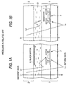
- One related technique of preventing ray penetration into the pixel transistor through the counter substrate comprises disposing a black matrix B adjacent to the counter substrate 2, as in Fig. 1A.
- the black matrix B acts to shield the pixel transistor from the incident rays.
- the present inventors previously proposed a technique of disposing a black matrix above the transistor on the side of the active substrate 1 facing the counter substrate 2, but not just below the counter substrate 2 to be adjacent thereto, as in Fig. 1B.
- the black matrix is nearer to the transistor, by which the incident rays going into the transistor could be reduced more effectively (see Japanese Patent Laid-Open No. 262494/1996).
- the incident rays L2 having scattered or reflected could be prevented from entering the pixel transistor 7.
- the black matrix is in two sites, both acting as a light-shielding layer.
- the active layer of the transistor is formed on the active substrate to be the lowermost layer thereon (opposite to the counter substrate). In this, therefore, the rays running toward the active substrate directly enter the active layer of the transistor, thereby causing photoelectric current leakage.
- the present invention is to solve the problems noted above, and its object is to provide a liquid crystal display device in which the incident rays having scattered and reflected and even the return rays as above are prevented from entering the transistor part and which is therefore free from the problem of photoelectric current leakage.
- the liquid crystal display device of the invention comprises an active substrate with a pixel transistor TFT thereon and a counter substrate that faces the active substrate via liquid crystal therebetween, wherein a light-shielding layer is formed both adjacent to the side of the pixel transistor part that faces the counter substrate and adjacent to the side thereof that faces opposite to the counter substrate and wherein the light-shielding layer that faces the counter substrate is in at least two sites relative to the incident rays running thereinto through the counter substrate so as to block all the incident rays toward the region except the pixel openings.
- the light-shielding layer that is in at least two sites is so constituted that it can block all rays toward the region except the pixel openings in the device.
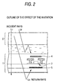
- the light-shielding layer is formed both adjacent to the side of the pixel transistor part that faces the counter substrate and adjacent to the side thereof that faces opposite to the counter substrate. Therefore, as graphically shown in Fig. 2, even the return rays (L3) can be blocked by the light-shielding layer (lower light-shielding layer 5) disposed on the side (light emitting side) opposite to the counter substrate, and the device is not troubled by photoelectric current leakage to be caused by the rays erroneously entering the pixel transistor part.
- a high-temperature polysilicon TFT as the pixel transistor, which, however, is not limitative.
- any other types of the device having, for example, a low-temperature polysilicon TFT or an a-silicon TFT could produce the same results as herein. (The same shall apply to the other embodiments to be mentioned hereunder.)
- Fig. 3 is referred to.
- an active matrix-type liquid crystal display device of one embodiment of the invention This comprises a substrate 1 with a pixel transistor TFT thereon (that is, the substrate 1 is of quartz, having TFT thereon), and a counter substrate 2 of, for example, glass.
- a liquid crystal component 3 of, for example, twisted namatic liquid crystal is sandwiched between the substrate 1 and the counter substrate 2.
- the counter substrate 2 is provided with a counter electrode 6 of, for example, ITO.
- the substrate 1 has a pixel electrode 8 of, for example, ITO, on a CMP-planarized layer 100 of, for example, an inorganic insulating film, while having a lower layer of TFT (thin film transistor) 7 below and adjacent to the layer 100.
- the TFT 7 is a top-gate-structured TFT, acting as a switching element for driving the pixel electrode 8.
- the TFT 7 has a thin semiconductor film 10 of polysilicon that acts as an active layer.
- the thin semiconductor film 10 is of a first polysilicon layer (1polySi).
- a gate G is formed on the thin semiconductor film 10 via a gate-insulating film 11 of SiO 2 or the like therebetween.
- the gate G is of a second polysilicon layer (2polySi).
- the TFT 7 has a source region S and a drain region D on both sides of the gate G.
- the source region S and the drain region D both have an LDD region at their facing ends, and are connected with lead electrodes 12A and 12B, respectively.
- the lead electrodes 12A and 12B are made of, for example, an aluminium material of aluminium or the like.
- the thin semiconductor film 10 has an auxiliary capacitance 13 (Cs) as formed therein.
- the auxiliary capacitance 13 (Cs) is formed of the first polysilicon layer (1polySi) that constitutes the thin semiconductor film 10 of TFT 7 and the second polysilicon layer (2polySi) that constitutes the thin semiconductor film 14 of gate G, via an insulating film of, for example, SiO 2 that constitutes the gate-insulating film 11 therebetween.
- light-shielding layers 4M and 4P are so positioned above the TFT 7 as to face the counter substrate 2, or that is, these are positioned on the side that receives the incident rays from a light source. As the case may be, they may be referred to as "upper light-shielding layers" or "first light-shielding layers”.
- the light-shielding mask layer 4M and the light-shielding pad layer 4P are the upper light-shielding layers, as illustrated.
- the incident rays that enter the device through the counter substrate are completely blocked by the two upper light-shielding layers (the light-shielding mask layer 4M and the light-shielding pad layer 4P) and by the lead electrodes 12A and 12B, overlapping with each other, (these are made of aluminium herein) in all regions except the pixel openings.
- the light-shielding mask layer 4M and the light-shielding pad layer 4P are both of a metal film of a conductive material of, for example, Ti or the like.
- the light-shielding mask layer 4M is patterned in series in the direction of pixel rows, at least partially shielding the TFT 7 from the rays running toward it.
- the light-shielding pad layer 4P is separately patterned for each pixel, being contacted with the pixel electrode. These light-shielding mask layer 4M, light-shielding pad layer 4P, and lead electrodes 12A and 12B, overlapping with each other, completely block the incident rays that enter the device through the counter substrate in all regions except the pixel openings.
- another light-shielding layer 5 is formed below the pixel transistor part on the side opposite to the counter substrate. As the case may be, this may be referred to as a "lower light-shielding layer” or “second light-shielding layer”. At least the facing source/drain edges in the pixel transistor are shielded from light by this lower light-shielding layer. In the thus-shielded source/drain edges, formed are the LDD regions 71 and 72 mentioned hereinabove.
- the lower light-shielding layer 5 is specifically designated by the shadow area.
- the reference numeral 10 indicates the first polysilicon layer for the pixel
- 141 indicates the second polysilicon layer for the gate line
- 142 indicates the second polysilicon layer for the auxiliary capacitance Cs
- 15 indicates a signal line (this is made of aluminium herein).
- the lower light-shielding layer 5 is made of a high-melting-point metal silicide.
- the layer 5 especially preferred is a film of WSi having a thickness of 200 nm.
- the lower light-shielding layer 5 is so patterned herein that it may shield at least the region of the facing source/drain edges ⁇ 2.0 ⁇ m in the pixel transistor (TFT 7) from the rays running toward it.
- the lower light-shielding layer 5 is earthed to GND.
- the region of the facing source/drain edges in the pixel transistor (TFT 7) to be shielded from the rays running toward it covers at least the edge of the gate G ⁇ 0.5 ⁇ m, more preferably ⁇ 1.0 ⁇ m.
- the lower light-shielding layer 5 may be so extended to the lower part below the channel region in the transistor moiety that it can integrally cover the channel region.
- the layer 5 may be extended to the region beyond the gate line of the pixel transistor. This is effective for relaxing the layer height difference in the pixel transistor structure and for reducing the stress to the gate line.
- the interconnection of that mode can be attained because the upper light-shielding layers noted above completely shield the pixel transistor in all regions except the pixel openings from the incident rays that enter the device.
- an insulating layer 9 of NSG having a thickness of 600 nm is layered over the lower light-shielding layer 5 through AP-CVD. Over the layer 9, further layered is polysilicon through LP-CVD. This is the first polysilicon layer (1polySi) for the thin semiconductor film 10, and forms the active layer for the TFT 7.
- the lower light-shielding layer 5 and the pixel transistor-forming layer are spaced by a thick film of the insulating layer 9 and that the film of the insulating layer 9 is as thick as possible like herein.
- the thickness of the film of the insulating layer 9 is not smaller than 100 nm, more preferably from 200 to 1500 nm.
- the insulating layer 9 is of NSG having a thickness of 600 nm as mentioned previously.
- the insulating layer may be of an SiO 2 film, an SiN film or the like to be formed through LP-CVD, AP-CVD or p-CVD.
- the insulating film 9 may be annealed for densifying its structure. Annealing the film 9 may be effected at 1000°C for 60 minutes or so, by which the lower light-shielding layer 5 could be prevented from being deteriorated in the subsequent steps.
- the lower light-shielding layer 5 has a low resistivity of not larger than 100 ⁇ /square, more preferably not larger than 10 ⁇ /square, in order not to be influenced so much by the coupling capacitance from the adjacent interconnections.
- the lower light-shielding layer 5 shall have a transmittance of generally not larger than 50 % at least for the light falling within a wavelength range of from 400 to 500 nm.
- the transmittance through the layer 5 is not larger than 10 %. More preferably, it is as small as possible, for ensuring higher light-shielding capabilities of the layer 5.
- the thickness of the lower light-shielding layer 5 is not specifically defined, provided that the layer 5 satisfies the requirements for the resistance and the light-shielding ability as above.
- the layer 5 may have a thickness of from 10 to 1000 nm, and preferably from 100 to 400 nm.
- high-melting-point metals and compounds of such metals are preferred for the material for the lower light-shielding layer 5.
- employable are W, Mo, Pt, Pd, Ti, Cr and their silicides.
- the light-shielding mask layer 4M shall have a fixed potential, which is, for example, equal to the potential of the counter electrode 6, while the light-shielding pad layer 4P shall be so interposed between the pixel electrode 8 and the lead electrode 12B as to enhance the electric connection between the two (see Fig. 3).
- These upper light-shielding layers could be so defined that their transmittance within a visible ray range of wavelength from 400 to 700 nm is not larger than 1 %, preferably not larger than 0.1 %.
- the material for the layers for example, employable are metals such as Cr, Ni, Ta, W, Al, Cu, Mo, Pt and Pd, in addition to Ti noted above, and also their alloys and silicides.
- the thickness of the layers is not specifically defined, provided that the layers satisfy the requirement for the intended light-shielding capabilities. In general, the layers may have a thickness of at least 50 nm.
- the light-shielding mask layer 4M and the light-shielding pad layer 4P may be made of the same material.
- the pixel transistor may have a double-gate structure. In that case, at least two source/drain edges in both the signal line area and the pixel area shall be shielded from light.
- driving circuit transistors for driving pixel transistors could be shielded from light in the same manner as herein.
- the transistors shielded from light could be protected from photo-carriers.
- This embodiment is the same as Embodiment 1, except that the lower light-shielding layer 5 is connected with the gate G in every stage.
- the lower light-shielding layer 5 is spaced from the active layer of the pixel transistor via the thick insulating film 9 of an NSG film as formed through AP-CVD, it will have a weak gate influence on the active layer of the thin semiconductor film 10 (first polysilicon layer, 1polySi) in Embodiment 1. Therefore, when the layer 5 is earthed to GND as in Embodiment 1, the ON current running through the transistor will decrease in some degree. As opposed to that, the lower light-shielding layer 5 is connected with the gate G in this embodiment, and the ON current reduction in the transistor could be prevented.
- the lower light-shielding layer 5 is spaced for each pixel unit into lower light-shielding layers 51, 52, ... each corresponding to each pixel unit.
- Each lower light-shielding layer shall be enough for completely covering the LDD regions in each transistor and shielding them from light, as in Embodiment 1.
- the lower light-shielding layers 51, 52, . . . are separately connected with the gate G in each pixel. The others are the same as in Embodiment 1.
- the liquid crystal display device of the invention is so constructed that the scattered or reflected incident rays and even the return rays are prevented from entering the transistor part. Therefore, the device is free from the problem of photoelectric current leakage.
Landscapes
- Physics & Mathematics (AREA)
- Nonlinear Science (AREA)
- Mathematical Physics (AREA)
- Engineering & Computer Science (AREA)
- Chemical & Material Sciences (AREA)
- Crystallography & Structural Chemistry (AREA)
- Microelectronics & Electronic Packaging (AREA)
- General Physics & Mathematics (AREA)
- Optics & Photonics (AREA)
- Liquid Crystal (AREA)
- Thin Film Transistor (AREA)
- Optical Elements Other Than Lenses (AREA)
- Devices For Indicating Variable Information By Combining Individual Elements (AREA)
Applications Claiming Priority (2)
| Application Number | Priority Date | Filing Date | Title |
|---|---|---|---|
| JP30746598 | 1998-10-28 | ||
| JP30746598A JP3141860B2 (ja) | 1998-10-28 | 1998-10-28 | 液晶表示装置の製造方法 |
Publications (2)
| Publication Number | Publication Date |
|---|---|
| EP0997769A2 true EP0997769A2 (fr) | 2000-05-03 |
| EP0997769A3 EP0997769A3 (fr) | 2002-08-07 |
Family
ID=17969410
Family Applications (1)
| Application Number | Title | Priority Date | Filing Date |
|---|---|---|---|
| EP99308296A Ceased EP0997769A3 (fr) | 1998-10-28 | 1999-10-21 | Dispositif d'affichage à cristal liquide et à matrice active |
Country Status (5)
| Country | Link |
|---|---|
| US (1) | US6327006B1 (fr) |
| EP (1) | EP0997769A3 (fr) |
| JP (1) | JP3141860B2 (fr) |
| KR (1) | KR100773872B1 (fr) |
| TW (1) | TW490586B (fr) |
Cited By (12)
| Publication number | Priority date | Publication date | Assignee | Title |
|---|---|---|---|---|
| GB2383178A (en) * | 2001-06-21 | 2003-06-18 | Esm Ltd | Opaque shielding element for liquid crystal display |
| US6583472B1 (en) | 1999-08-31 | 2003-06-24 | Semiconductor Energy Laboratory Co., Ltd. | Semiconductor device and method of manufacturing thereof |
| GB2383460A (en) * | 2001-06-21 | 2003-06-25 | Esm Ltd | Optical masking layer for LCD display |
| EP1180716A3 (fr) * | 2000-08-10 | 2003-10-01 | Sony Corporation | Dispositif semi-conducteur à couches minces et unité d'affichage à cristaux liquides et leurs procédés de fabrication |
| US6680488B2 (en) | 2001-04-20 | 2004-01-20 | Semiconductor Energy Laboratory Co., Ltd. | Semiconductor device |
| EP1279997A3 (fr) * | 2001-07-23 | 2004-09-01 | Nec Corporation | Dispositif d'affichage à cristaux liquides |
| US7075594B2 (en) | 2002-07-09 | 2006-07-11 | Sharp Kabushiki Kaisha | Liquid crystal display device with side light shielding layers and method for producing the same |
| US7163848B2 (en) | 2000-06-28 | 2007-01-16 | Semiconductor Energy Laboratory Co., Ltd. | Semiconductor device and manufacturing method thereof |
| US7218361B2 (en) | 2000-03-27 | 2007-05-15 | Semiconductor Energy Laboratory Co., Ltd. | Semiconductor display device and manufacturing method thereof |
| US7465957B2 (en) | 2001-09-26 | 2008-12-16 | Semiconductor Energy Laboratory Co., Ltd. | Semiconductor device |
| US7541618B2 (en) | 1999-09-27 | 2009-06-02 | Semiconductor Energy Laboratory Co., Ltd. | Liquid crystal device having a thin film transistor |
| US8551796B2 (en) | 2000-09-29 | 2013-10-08 | Semiconductor Energy Laboratory Co., Ltd. | Semiconductor device and its manufacturing method |
Families Citing this family (61)
| Publication number | Priority date | Publication date | Assignee | Title |
|---|---|---|---|---|
| JP3716580B2 (ja) | 1997-02-27 | 2005-11-16 | セイコーエプソン株式会社 | 液晶装置及びその製造方法、並びに投写型表示装置 |
| US6850292B1 (en) * | 1998-12-28 | 2005-02-01 | Seiko Epson Corporation | Electric-optic device, method of fabricating the same, and electronic apparatus |
| KR100628679B1 (ko) * | 1999-11-15 | 2006-09-28 | 엘지.필립스 엘시디 주식회사 | 어레이 패널, 액정 표시장치 제조방법 및 그 제조방법에따른액정표시장치 |
| CN1267782C (zh) | 2000-04-21 | 2006-08-02 | 精工爱普生株式会社 | 电光装置 |
| KR100367009B1 (ko) * | 2000-05-19 | 2003-01-09 | 엘지.필립스 엘시디 주식회사 | 액정표시소자 및 그 제조방법 |
| JP2002026030A (ja) * | 2000-07-05 | 2002-01-25 | Sony Corp | 半導体装置およびその製造方法 |
| JP3823016B2 (ja) * | 2000-07-21 | 2006-09-20 | 株式会社日立製作所 | 液晶表示装置 |
| JP4896314B2 (ja) * | 2000-08-04 | 2012-03-14 | 株式会社半導体エネルギー研究所 | 表示装置 |
| US6982194B2 (en) * | 2001-03-27 | 2006-01-03 | Semiconductor Energy Laboratory Co., Ltd. | Semiconductor device and method for manufacturing the same |
| US7189997B2 (en) | 2001-03-27 | 2007-03-13 | Semiconductor Energy Laboratory Co., Ltd. | Semiconductor device and method for manufacturing the same |
| JP4210041B2 (ja) * | 2001-03-30 | 2009-01-14 | 東京エレクトロン株式会社 | 熱処理装置 |
| JP2002299632A (ja) * | 2001-03-30 | 2002-10-11 | Sanyo Electric Co Ltd | 半導体装置及びアクティブマトリクス型表示装置 |
| US6740938B2 (en) | 2001-04-16 | 2004-05-25 | Semiconductor Energy Laboratory Co., Ltd. | Transistor provided with first and second gate electrodes with channel region therebetween |
| JP4306142B2 (ja) * | 2001-04-24 | 2009-07-29 | 株式会社日立製作所 | 画像表示装置及びその製造方法 |
| JP4731718B2 (ja) * | 2001-04-27 | 2011-07-27 | 株式会社半導体エネルギー研究所 | 表示装置 |
| US6734463B2 (en) * | 2001-05-23 | 2004-05-11 | Semiconductor Energy Laboratory Co., Ltd. | Semiconductor device comprising a window |
| US6906344B2 (en) | 2001-05-24 | 2005-06-14 | Semiconductor Energy Laboratory Co., Ltd. | Thin film transistor with plural channels and corresponding plural overlapping electrodes |
| FR2826766B1 (fr) * | 2001-06-29 | 2003-10-31 | Thales Avionics Lcd | Matrice active de transistors en couches minces ou tft pour capteur optique ou ecran de visualisation |
| US6952023B2 (en) | 2001-07-17 | 2005-10-04 | Semiconductor Energy Laboratory Co., Ltd. | Light emitting device |
| KR100803566B1 (ko) * | 2001-07-25 | 2008-02-15 | 엘지.필립스 엘시디 주식회사 | 액정 표시 장치용 어레이 기판 및 그의 제조 방법 |
| KR100802445B1 (ko) * | 2001-07-30 | 2008-02-13 | 엘지.필립스 엘시디 주식회사 | 반사투과형 액정표시장치용 어레이기판과 그 제조방법 |
| US7027109B2 (en) | 2001-08-03 | 2006-04-11 | Nec Corporation | TFT array substrate and active-matrix addressing liquid-crystal display device |
| TWI244571B (en) * | 2002-01-30 | 2005-12-01 | Sanyo Electric Co | Semiconductor display device |
| TW594336B (en) * | 2002-01-30 | 2004-06-21 | Sanyo Electric Co | Semiconductor display device, method for making the same, and active matrix type display device |
| KR20030068667A (ko) * | 2002-02-15 | 2003-08-25 | 엘지전자 주식회사 | 반사형 액정표시소자 |
| JP4216092B2 (ja) * | 2002-03-08 | 2009-01-28 | 株式会社半導体エネルギー研究所 | 液晶表示装置 |
| JP2003332045A (ja) * | 2002-05-09 | 2003-11-21 | Sanyo Electric Co Ltd | エレクトロルミネッセンス表示装置及びその製造方法 |
| JP4341062B2 (ja) * | 2003-02-12 | 2009-10-07 | 日本電気株式会社 | 薄膜トランジスタおよびその製造方法 |
| JP4069906B2 (ja) * | 2003-08-04 | 2008-04-02 | セイコーエプソン株式会社 | 電気光学装置及びその製造方法並びに電子機器 |
| JP2005092122A (ja) | 2003-09-19 | 2005-04-07 | Nec Corp | 薄膜トランジスタ基板及びその製造方法 |
| US20060187393A1 (en) * | 2005-02-23 | 2006-08-24 | Da-Shuang Kuan | Liquid crystal panel and liquid crystal projection device using thereof |
| KR101109623B1 (ko) * | 2005-04-07 | 2012-01-31 | 엘지디스플레이 주식회사 | 박막트랜지스터와 그 제조방법. |
| JP5135667B2 (ja) * | 2005-08-29 | 2013-02-06 | セイコーエプソン株式会社 | 電気光学装置及びプロジェクタ |
| JP2007103584A (ja) * | 2005-10-03 | 2007-04-19 | Ricoh Co Ltd | トランジスタ素子、表示装置およびこれらの製造方法 |
| JP2007188936A (ja) * | 2006-01-11 | 2007-07-26 | Epson Imaging Devices Corp | 表示装置 |
| KR101338109B1 (ko) * | 2006-12-29 | 2013-12-06 | 엘지디스플레이 주식회사 | 액정표시소자 |
| TWI358832B (en) * | 2007-02-26 | 2012-02-21 | Au Optronics Corp | Semiconductor device and manufacturing method ther |
| JP5044273B2 (ja) * | 2007-04-27 | 2012-10-10 | 三菱電機株式会社 | 薄膜トランジスタアレイ基板、その製造方法、及び表示装置 |
| JP5018336B2 (ja) | 2007-08-22 | 2012-09-05 | セイコーエプソン株式会社 | 電気光学装置及び電子機器 |
| JP2009058717A (ja) * | 2007-08-31 | 2009-03-19 | Seiko Epson Corp | 電気光学装置及びその製造方法、並びに電子機器 |
| US8896065B2 (en) * | 2008-04-14 | 2014-11-25 | Sharp Laboratories Of America, Inc. | Top gate thin film transistor with independent field control for off-current suppression |
| JP5491833B2 (ja) * | 2008-12-05 | 2014-05-14 | 株式会社半導体エネルギー研究所 | 半導体装置 |
| TWI458098B (zh) * | 2009-12-31 | 2014-10-21 | 友達光電股份有限公司 | 薄膜電晶體 |
| JP5284538B2 (ja) * | 2010-04-16 | 2013-09-11 | シャープ株式会社 | 電子基板の製造方法、液晶表示装置の製造方法、電子基板、及び、液晶表示装置 |
| KR102089468B1 (ko) * | 2012-09-04 | 2020-03-16 | 엘지디스플레이 주식회사 | 금속 산화물 반도체 층을 차광하는 광 흡수층을 구비한 박막 트랜지스터 기판 및 그 제조 방법 |
| CN104022126B (zh) * | 2014-05-28 | 2017-04-12 | 京东方科技集团股份有限公司 | 一种阵列基板、其制作方法及显示装置 |
| KR20160084550A (ko) | 2015-01-05 | 2016-07-14 | 삼성디스플레이 주식회사 | 표시 장치 및 그 제조 방법 |
| TWI638206B (zh) | 2015-09-01 | 2018-10-11 | 友達光電股份有限公司 | 主動元件陣列基板 |
| JP2018054941A (ja) * | 2016-09-29 | 2018-04-05 | パナソニック液晶ディスプレイ株式会社 | 液晶表示装置 |
| CN107946337B (zh) | 2016-10-12 | 2020-07-10 | 群创光电股份有限公司 | 显示设备 |
| JP2018116107A (ja) * | 2017-01-17 | 2018-07-26 | 株式会社ジャパンディスプレイ | 表示装置 |
| CN106684103B (zh) * | 2017-02-28 | 2020-04-03 | 厦门天马微电子有限公司 | 阵列基板、显示面板及显示装置 |
| CN107275347B (zh) * | 2017-06-30 | 2020-06-23 | 京东方科技集团股份有限公司 | 一种阵列基板、其制备方法及显示面板 |
| US20240021629A1 (en) * | 2018-04-27 | 2024-01-18 | Boe Technology Group Co., Ltd. | Array substrate, method of manufacturing the same and method of improving performance of the same, display panel and display device |
| JP2018170510A (ja) * | 2018-06-04 | 2018-11-01 | 株式会社半導体エネルギー研究所 | 半導体装置 |
| KR102819878B1 (ko) * | 2019-03-15 | 2025-06-12 | 삼성디스플레이 주식회사 | 표시 장치 |
| JP2020126250A (ja) * | 2020-03-30 | 2020-08-20 | セイコーエプソン株式会社 | 電気光学装置および電子機器 |
| CN115172417A (zh) * | 2022-06-17 | 2022-10-11 | 合肥维信诺科技有限公司 | 显示面板及其制备方法、显示装置 |
| CN116544245B (zh) * | 2023-06-29 | 2023-09-22 | 绵阳惠科光电科技有限公司 | 阵列基板及其制备方法、显示面板 |
| CN116581131B (zh) | 2023-07-10 | 2024-01-30 | 惠科股份有限公司 | 阵列基板及其制备方法、显示面板 |
| CN118192128A (zh) * | 2024-03-13 | 2024-06-14 | 武汉华星光电技术有限公司 | 阵列基板和显示面板 |
Citations (2)
| Publication number | Priority date | Publication date | Assignee | Title |
|---|---|---|---|---|
| EP0136509A2 (fr) * | 1983-08-23 | 1985-04-10 | Kabushiki Kaisha Toshiba | Dispositif d'affichage actif du type à matrice |
| EP0481734A2 (fr) * | 1990-10-16 | 1992-04-22 | Agency Of Industrial Science And Technology | Dispositif obturateur de lumière |
Family Cites Families (16)
| Publication number | Priority date | Publication date | Assignee | Title |
|---|---|---|---|---|
| JP3307150B2 (ja) * | 1995-03-20 | 2002-07-24 | ソニー株式会社 | アクティブマトリクス型表示装置 |
| JPS58159520A (ja) * | 1982-03-18 | 1983-09-21 | Seiko Epson Corp | 液晶表示パネル |
| JPS60213062A (ja) * | 1984-04-09 | 1985-10-25 | Hosiden Electronics Co Ltd | 薄膜トランジスタの製造方法 |
| JP3143996B2 (ja) * | 1991-10-08 | 2001-03-07 | ソニー株式会社 | 液晶表示装置 |
| JPH05249478A (ja) * | 1991-12-25 | 1993-09-28 | Toshiba Corp | 液晶表示装置 |
| JP3526058B2 (ja) * | 1992-08-19 | 2004-05-10 | セイコーインスツルメンツ株式会社 | 光弁用半導体装置 |
| US5412493A (en) * | 1992-09-25 | 1995-05-02 | Sony Corporation | Liquid crystal display device having LDD structure type thin film transistors connected in series |
| JP2739844B2 (ja) * | 1995-05-19 | 1998-04-15 | 日本電気株式会社 | 薄膜トランジスタアレイ |
| JPH0980476A (ja) * | 1995-09-12 | 1997-03-28 | Nec Corp | アクティブマトリックス基板とその製造方法 |
| KR100186548B1 (ko) * | 1996-01-15 | 1999-05-01 | 구자홍 | 액정표시장치의 구조 |
| JPH09311342A (ja) * | 1996-05-16 | 1997-12-02 | Semiconductor Energy Lab Co Ltd | 表示装置 |
| JP3708637B2 (ja) * | 1996-07-15 | 2005-10-19 | 株式会社半導体エネルギー研究所 | 液晶表示装置 |
| TWI236556B (en) | 1996-10-16 | 2005-07-21 | Seiko Epson Corp | Substrate for a liquid crystal equipment, liquid crystal equipment and projection type display equipment |
| US5879959A (en) * | 1997-01-17 | 1999-03-09 | Industrial Technology Research Institute | Thin-film transistor structure for liquid crystal display |
| US6232142B1 (en) * | 1997-12-09 | 2001-05-15 | Seiko Epson Corporation | Semiconductor device and method for making the same, electro-optical device using the same and method for making the electro-optical device, and electronic apparatus using the electro-optical device |
| JP2000075280A (ja) * | 1998-08-28 | 2000-03-14 | Sony Corp | 液晶表示装置 |
-
1998
- 1998-10-28 JP JP30746598A patent/JP3141860B2/ja not_active Expired - Fee Related
-
1999
- 1999-10-12 TW TW088117578A patent/TW490586B/zh not_active IP Right Cessation
- 1999-10-19 KR KR1019990045197A patent/KR100773872B1/ko not_active Expired - Lifetime
- 1999-10-21 EP EP99308296A patent/EP0997769A3/fr not_active Ceased
- 1999-10-27 US US09/427,735 patent/US6327006B1/en not_active Expired - Lifetime
Patent Citations (2)
| Publication number | Priority date | Publication date | Assignee | Title |
|---|---|---|---|---|
| EP0136509A2 (fr) * | 1983-08-23 | 1985-04-10 | Kabushiki Kaisha Toshiba | Dispositif d'affichage actif du type à matrice |
| EP0481734A2 (fr) * | 1990-10-16 | 1992-04-22 | Agency Of Industrial Science And Technology | Dispositif obturateur de lumière |
Cited By (29)
| Publication number | Priority date | Publication date | Assignee | Title |
|---|---|---|---|---|
| US9250490B2 (en) | 1999-08-31 | 2016-02-02 | Semiconductor Energy Laboratory Co., Ltd. | Liquid crystal display device including light shielding film |
| US7098086B2 (en) | 1999-08-31 | 2006-08-29 | Semiconductor Energy Laboratory Co., Ltd. | Semiconductor device and method of manufacturing thereof |
| US8552431B2 (en) | 1999-08-31 | 2013-10-08 | Semiconductor Energy Laboratory Co., Ltd. | Semiconductor device comprising pixel portion |
| US7501685B2 (en) | 1999-08-31 | 2009-03-10 | Semiconductor Energy Laboratory Co., Ltd. | Display device comprising pixel portion |
| US7982267B2 (en) | 1999-08-31 | 2011-07-19 | Semiconductor Energy Laboratory Co., Ltd. | Projector including display device |
| US8253140B2 (en) | 1999-08-31 | 2012-08-28 | Semiconductor Energy Laboratory Co., Ltd. | Display device having capacitor wiring |
| US9466622B2 (en) | 1999-08-31 | 2016-10-11 | Semiconductor Energy Laboratory Co., Ltd. | Display device comprising a thin film transistor and a storage capacitor |
| US8933455B2 (en) | 1999-08-31 | 2015-01-13 | Semiconductor Energy Laboratory Co., Ltd. | Display device comprising pixel |
| US6583472B1 (en) | 1999-08-31 | 2003-06-24 | Semiconductor Energy Laboratory Co., Ltd. | Semiconductor device and method of manufacturing thereof |
| US7541618B2 (en) | 1999-09-27 | 2009-06-02 | Semiconductor Energy Laboratory Co., Ltd. | Liquid crystal device having a thin film transistor |
| US7218361B2 (en) | 2000-03-27 | 2007-05-15 | Semiconductor Energy Laboratory Co., Ltd. | Semiconductor display device and manufacturing method thereof |
| US7486344B2 (en) | 2000-03-27 | 2009-02-03 | Semiconductor Energy Laboratory Co., Ltd. | Semiconductor display device and manufacturing method thereof |
| US7163848B2 (en) | 2000-06-28 | 2007-01-16 | Semiconductor Energy Laboratory Co., Ltd. | Semiconductor device and manufacturing method thereof |
| US7514302B2 (en) | 2000-06-28 | 2009-04-07 | Semiconductor Energy Laboratory Co., Ltd. | Semiconductor device and manufacturing method thereof |
| EP1180716A3 (fr) * | 2000-08-10 | 2003-10-01 | Sony Corporation | Dispositif semi-conducteur à couches minces et unité d'affichage à cristaux liquides et leurs procédés de fabrication |
| US8551796B2 (en) | 2000-09-29 | 2013-10-08 | Semiconductor Energy Laboratory Co., Ltd. | Semiconductor device and its manufacturing method |
| US6680488B2 (en) | 2001-04-20 | 2004-01-20 | Semiconductor Energy Laboratory Co., Ltd. | Semiconductor device |
| GB2383178B (en) * | 2001-06-21 | 2005-07-27 | Esm Ltd | Opaque shielding element for liquid crystal display |
| GB2383178A (en) * | 2001-06-21 | 2003-06-18 | Esm Ltd | Opaque shielding element for liquid crystal display |
| GB2383460B (en) * | 2001-06-21 | 2005-11-30 | Esm Ltd | Optical masking layer for LCD display |
| GB2383460A (en) * | 2001-06-21 | 2003-06-25 | Esm Ltd | Optical masking layer for LCD display |
| EP1744206A3 (fr) * | 2001-07-23 | 2007-04-04 | NEC Corporation | Dispositif d'affichage à cristaux liquides |
| EP1744206A2 (fr) | 2001-07-23 | 2007-01-17 | NEC Corporation | Dispositif d'affichage à cristaux liquides |
| EP1279997A3 (fr) * | 2001-07-23 | 2004-09-01 | Nec Corporation | Dispositif d'affichage à cristaux liquides |
| US7465957B2 (en) | 2001-09-26 | 2008-12-16 | Semiconductor Energy Laboratory Co., Ltd. | Semiconductor device |
| US8502231B2 (en) | 2001-09-26 | 2013-08-06 | Semiconductor Energy Laboratory Co., Ltd. | Semiconductor device |
| US8183569B2 (en) | 2001-09-26 | 2012-05-22 | Semiconductor Energy Laboratory Co., Ltd. | Semiconductor device |
| US7939827B2 (en) | 2001-09-26 | 2011-05-10 | Semiconductor Energy Laboratory Co., Ltd. | Semiconductor device |
| US7075594B2 (en) | 2002-07-09 | 2006-07-11 | Sharp Kabushiki Kaisha | Liquid crystal display device with side light shielding layers and method for producing the same |
Also Published As
| Publication number | Publication date |
|---|---|
| US6327006B1 (en) | 2001-12-04 |
| KR100773872B1 (ko) | 2007-11-06 |
| TW490586B (en) | 2002-06-11 |
| JP2000131716A (ja) | 2000-05-12 |
| JP3141860B2 (ja) | 2001-03-07 |
| EP0997769A3 (fr) | 2002-08-07 |
| KR20000029160A (ko) | 2000-05-25 |
Similar Documents
| Publication | Publication Date | Title |
|---|---|---|
| US6327006B1 (en) | TFT-LCD having shielding layers on TFT-substrate | |
| JP3307181B2 (ja) | 透過型表示装置 | |
| KR100918138B1 (ko) | 표시 장치 및 그 제조 방법 | |
| JP3918412B2 (ja) | 薄膜半導体装置及び液晶表示装置とこれらの製造方法 | |
| KR100408793B1 (ko) | 액티브매트릭스형표시장치 | |
| KR970000359B1 (ko) | 액정표시장치 | |
| US6259200B1 (en) | Active-matrix display apparatus | |
| CN101009333B (zh) | 半导体装置 | |
| US12085823B2 (en) | Display device and semiconductor device | |
| CN100526962C (zh) | 显示装置及其制造方法 | |
| EP1282001A2 (fr) | Substrat à matrice active et dispositif d'affichage à cristaux liquides à matrice active | |
| KR100746140B1 (ko) | 액정표시장치용 어레이기판과 그 제조방법 | |
| JP3796072B2 (ja) | 透過型液晶表示装置 | |
| JP2000330132A (ja) | アクティブマトリクス型表示装置 | |
| JP3750303B2 (ja) | 液晶表示装置 | |
| US7167218B1 (en) | Liquid crystal display and method of manufacture | |
| JP3371192B2 (ja) | 液晶表示装置 | |
| JP4496600B2 (ja) | 電気光学装置及びプロジェクタ | |
| JP2000047254A (ja) | 液晶表示装置 | |
| JP2000206562A (ja) | 液晶表示装置 | |
| KR101405367B1 (ko) | 액정표시장치와 그 제조방법 | |
| JPH07248507A (ja) | 液晶表示装置 | |
| JP2003098515A (ja) | 液晶表示装置及びそれを用いたプロジェクタ | |
| JP2006178235A (ja) | 薄膜トランジスタアレイ基板及び液晶表示装置 | |
| US8264628B2 (en) | Capacitor element, method for manufacturing the same, and electro-optic device |
Legal Events
| Date | Code | Title | Description |
|---|---|---|---|
| PUAI | Public reference made under article 153(3) epc to a published international application that has entered the european phase |
Free format text: ORIGINAL CODE: 0009012 |
|
| AK | Designated contracting states |
Kind code of ref document: A2 Designated state(s): AT BE CH CY DE DK ES FI FR GB GR IE IT LI LU MC NL PT SE |
|
| AX | Request for extension of the european patent |
Free format text: AL;LT;LV;MK;RO;SI |
|
| PUAL | Search report despatched |
Free format text: ORIGINAL CODE: 0009013 |
|
| AK | Designated contracting states |
Kind code of ref document: A3 Designated state(s): AT BE CH CY DE DK ES FI FR GB GR IE IT LI LU MC NL PT SE |
|
| AX | Request for extension of the european patent |
Free format text: AL;LT;LV;MK;RO;SI |
|
| 17P | Request for examination filed |
Effective date: 20030109 |
|
| 17Q | First examination report despatched |
Effective date: 20030224 |
|
| AKX | Designation fees paid |
Designated state(s): DE GB NL |
|
| APBN | Date of receipt of notice of appeal recorded |
Free format text: ORIGINAL CODE: EPIDOSNNOA2E |
|
| APBT | Appeal procedure closed |
Free format text: ORIGINAL CODE: EPIDOSNNOA9E |
|
| STAA | Information on the status of an ep patent application or granted ep patent |
Free format text: STATUS: THE APPLICATION HAS BEEN REFUSED |
|
| APAF | Appeal reference modified |
Free format text: ORIGINAL CODE: EPIDOSCREFNE |
|
| 18R | Application refused |
Effective date: 20050812 |