EP0997929A1 - Plasmaätzen von Polymermaterialien - Google Patents
Plasmaätzen von Polymermaterialien Download PDFInfo
- Publication number
- EP0997929A1 EP0997929A1 EP98402724A EP98402724A EP0997929A1 EP 0997929 A1 EP0997929 A1 EP 0997929A1 EP 98402724 A EP98402724 A EP 98402724A EP 98402724 A EP98402724 A EP 98402724A EP 0997929 A1 EP0997929 A1 EP 0997929A1
- Authority
- EP
- European Patent Office
- Prior art keywords
- polymer material
- etching
- layer
- mask
- plasma
- Prior art date
- Legal status (The legal status is an assumption and is not a legal conclusion. Google has not performed a legal analysis and makes no representation as to the accuracy of the status listed.)
- Withdrawn
Links
Images

Classifications
-
- H—ELECTRICITY
- H10—SEMICONDUCTOR DEVICES; ELECTRIC SOLID-STATE DEVICES NOT OTHERWISE PROVIDED FOR
- H10P—GENERIC PROCESSES OR APPARATUS FOR THE MANUFACTURE OR TREATMENT OF DEVICES COVERED BY CLASS H10
- H10P50/00—Etching of wafers, substrates or parts of devices
- H10P50/73—Etching of wafers, substrates or parts of devices using masks for insulating materials
-
- H—ELECTRICITY
- H10—SEMICONDUCTOR DEVICES; ELECTRIC SOLID-STATE DEVICES NOT OTHERWISE PROVIDED FOR
- H10P—GENERIC PROCESSES OR APPARATUS FOR THE MANUFACTURE OR TREATMENT OF DEVICES COVERED BY CLASS H10
- H10P50/00—Etching of wafers, substrates or parts of devices
- H10P50/20—Dry etching; Plasma etching; Reactive-ion etching
- H10P50/28—Dry etching; Plasma etching; Reactive-ion etching of insulating materials
- H10P50/286—Dry etching; Plasma etching; Reactive-ion etching of insulating materials of organic materials
- H10P50/287—Dry etching; Plasma etching; Reactive-ion etching of insulating materials of organic materials by chemical means
-
- H—ELECTRICITY
- H10—SEMICONDUCTOR DEVICES; ELECTRIC SOLID-STATE DEVICES NOT OTHERWISE PROVIDED FOR
- H10P—GENERIC PROCESSES OR APPARATUS FOR THE MANUFACTURE OR TREATMENT OF DEVICES COVERED BY CLASS H10
- H10P14/00—Formation of materials, e.g. in the shape of layers or pillars
- H10P14/60—Formation of materials, e.g. in the shape of layers or pillars of insulating materials
- H10P14/68—Organic materials, e.g. photoresists
- H10P14/683—Organic materials, e.g. photoresists carbon-based polymeric organic materials, e.g. polyimides, poly cyclobutene or PVC
Definitions
- the present invention generally pertains to a method for fabricating semiconductor devices. More particularly, the present invention concerns a method for etching a polymer, which polymer can typically be used as a dielectric insulating layer in a semiconductor device.
- Front end which consists, for example, of transistors, various p and/or n junctions, buried structures, etc.
- back end which connects the different parts of the lower active area between each other.
- the back end of the semiconductor devices includes patterned metal layers separated with each other by insulating dielectric layers. Contact holes are formed in the insulating dielectric layers and filled with metal so as to enable connection of the various patterned metal layers with each other and with the lower active area of the device, thereby ensuring the appropriate electrical connections between the different parts of the lower active area.
- Each patterned metal layer typically consists of one or several metal lines located in a same plane. These lines can be formed by etching a dielectric layer so as to form slots therethrough, and filling the slots with metal.
- a dry etching technique In order to form contact holes and/or slots in a given dielectric layer, the latter is etched according to a predetermined pattern.
- a dry etching technique can be used.
- Known dry etching techniques involve the use of a plasma etching chamber comprising, notably, two electrodes and a Radio-Frequency power supply, and containing a gas mixture.
- a wafer comprising a dielectric layer to be etched, is introduced into the etching chamber.
- the RF power supply generates a glow discharge in the gas mixture between the two electrodes so as to produce a plasma.
- the plasma etches the dielectric layer by way of appropriate chemical reactions which take place between particular compounds of the plasma and the dielectric layer material.
- the plasma generation is accompanied by an ion bombardment which enhances the etching operation.
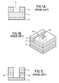
- FIGS 1A, 1B and 1C diagrammatically show a prior art method for etching a dielectric material layer using a plasma.
- the dielectric layer designated by reference numeral 1
- the dielectric layer is supported by a substrate 2.
- a mask, or resist, 3 is formed on the dielectric layer 1.
- the mask 3 is patterned in such a manner that apertures 4, such as through-holes 4a and slots 4b, be defined therethrough, as shown in perspective view on figure 1B.
- the wafer comprising layers 1, 2 and 3 is placed inside the etching chamber (not shown).
- the plasma generated in the chamber etches the dielectric layer 1 through the apertures 4, in order for the pattern defined in the mask 3 to be transferred to the dielectric layer 1 (see figure 1C). Then the mask 3 is removed from the wafer.
- the dielectric layer 1 is composed of a mineral material, typically silicon oxide (SiO 2 ), whereas the mask 3 is composed of an organic material.
- the plasma selectively etches the dielectric material, i.e., the plasma etches the dielectric layer 1 without eroding the mask 3 too much. Indeed, if the mask 3 is damaged during the etching process, the pattern defined therein will be modified and an accurate etching of the dielectric layer will not be possible.
- the etching process be anisotropic.
- An etching process is anisotropic when the dielectric material is etched in a single direction, which is normal to the surface of the wafer. In such a case, the side walls 1a (figure 1C) resulting from the etching process remain substantially straight and are not etched in a lateral direction.
- Anisotropic etching is preferred over isotropic etching when a great accuracy is required in the manufacturing of the semiconductor device.
- the present invention aims to satisfy these needs.
- a method for etching a polymer material characterised in that it comprises the steps of forming a first mask comprising a mineral material on said polymer material, said first mask having a pattern etched therein; generating a plasma from a gas mixture comprising oxygen and sulphur-bearing gas such as sulphur dioxide; and etching said polymer material using said plasma so as to transfer said pattern to said polymer material.
- the first mask which comprises a mineral material
- the polymer material can therefore be selectively etched.
- a gas mixture comprising oxygen and sulphur-bearing gas such as sulphur dioxide and a mask comprising a mineral material
- the present invention makes it possible to fabricate semiconductor devices with great accuracy.
- the polymer material is etched by the chemical action of the plasma, which is accompanied by an ion bombardment directed towards the surface of the polymer material. More precisely, the oxygen atoms contained in the plasma chemically react with the polymer to form volatile species, thereby removing portions of the polymer material.
- the sulphur dioxide chemically reacts with the polymer to form non-volatile species, such as C x S y and more particularly CS 2 , which protect the sidewalls of the apertures being formed in the polymer material from the etching process. Anisotropic etching can thus be carried out.
- the ion bombardment removes the non-volatile species deposited on the bottom of the apertures being formed, thus avoiding the risk of etch stop which could occur if a CS 2 layer was to remain on the polymer surface portions to be etched.
- the gas mixture further comprises a carrier gas, such as argon.
- a carrier gas such as argon.
- the polymer material to be etched can further comprise a mineral compound, such as silicon.
- the gas mixture further comprises at least one fluorine-based compound.
- the step of forming the first mask comprises the steps of: forming a first layer comprising a mineral material on the polymer material; forming a second mask comprising a polymer material on said first layer, said second mask having said pattern etched therein; and etching the first layer so as to transfer said pattern to the first layer.
- the step of etching the first layer typically uses a plasma etching technique.
- the step of forming the second mask comprises the steps of: forming a second layer comprising a polymer material on said first layer; and etching the second layer so as to produce said pattern.
- the step of etching the second layer uses a lithography technique.
- the second mask is removed during the step of etching the polymer material. No particular additional treatment is then required to remove the second mask.
- a polymer material layer to be etched 6 is formed on a substrate 5 (figure 2A).
- substrate we mean here an underlying layer, i.e., a layer which is formed before the polymer material layer 6 during the manufacturing of a semiconductor device.
- the polymer material which composes the layer 6 is, for example, the SiLK (Registered Trademark) material commercialised by the DOW CHEMICAL COMPANY.
- a mineral material layer 7 is formed on the polymer material layer 6 (figure 2B).
- the mineral material which composes the layer 7 is, for example, silicon oxide (SiO 2 ).
- a photoresist polymer material layer 8 is formed on the mineral material layer 7 (figure 2C).
- the layers 6, 7 and 8 are formed using conventional techniques, such as the spin coating technique or the PECVD (Plasma Enhanced Chemical Vapour Deposition) technique.
- the photoresist polymer material layer 8 is patterned by lithography so as to form a mask 8a (figure 2D).
- the mask 8a comprises through-holes and/or slots 8b, which define the respective locations of the contact holes and/or slots to be formed in the polymer material layer 6.
- a dry etching method is applied to the wafer 5, 6, 7, 8a such that the pattern defined in the mask 8a be transferred to the mineral material layer 7 to form a mineral material mask 7a, called "hard mask” (figure 2E).
- the dry etching method used at the fifth step is a plasma etching method, of the type conventionally used for etching mineral material layers, such as SiO 2 layers, through polymer material masks.
- a plasma etching method of the type conventionally used for etching mineral material layers, such as SiO 2 layers, through polymer material masks.
- Such a method is described, for example, in US-A-5,595,627. It generally consists in placing the wafer in a plasma chamber and generating a plasma from a gas mixture comprising, notably, carbo-fluorinated compounds (C x F y ).
- the carbo-fluorinated compounds chemically react with the silicon oxide composing the mineral material layer.
- the species obtained by such a chemical reaction are volatile, so that the mineral material layer is etched by removal of portions thereof.
- the plasma chamber is configured such that the plasma etching process be accompanied by an ion bombardment directed towards the wafer, as shown by arrows 9 on figure 2D.
- the plasma etching chamber used by the present invention is of the type described in US-A-5,717,294.
- the pattern defined in the mineral material mask 7a is transferred to the polymer material layer 6 according to the method described herebelow.
- the gas mixture which was used for performing the fifth step is output from the plasma etching chamber.
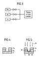
- Another gas mixture comprising sulphur dioxide (SO 2 ), oxygen (O 2 ) and argon (Ar), is then supplied into the plasma chamber, as shown on figure 3.
- a plasma is generated from the latter gas mixture while the wafer is disposed in the plasma chamber.
- the operation parameters of the plasma chamber are selected such that an ion bombardment be directed towards the wafer.
- the oxygen atoms (O) resulting from the dissociation of the oxygen (O 2 ) and the sulphur dioxide (SO 2 ) in the plasma etches the polymer material by chemically reacting with the carbon of the polymer to form volatile (gaseous) species.
- oxygen atoms (O) resulting from the dissociation of the oxygen (O 2 ) and the sulphur dioxide (SO 2 ) in the plasma etches the polymer material by chemically reacting with the carbon of the polymer to form volatile (gaseous) species.
- a problem which may occur when using oxygen as an etching element is that the oxygen not only etches the polymer material in a direction normal to the surface thereof, but also in a direction parallel to such surface.
- the side walls 6c of the apertures (contact holes and/or slots) resulting from the etching process are then curved, as shown in figure 4.
- the sulphur dioxide (SO 2 ) contained in the gas mixture makes it possible to avoid this problem. Indeed, during the etching process, the sulphur dioxide chemically reacts with the carbon of the polymer material to form a CS 2 layer on the bottom 6d and the side walls 6e of the apertures being formed, as diagrammatically shown on figure 5.
- the ion bombardment, illustrated at 10 on figure 5, which accompanies the chemical action of the plasma removes the CS 2 layer present on the aperture bottom 6d, while leaving the CS 2 layer formed on the side walls 6e unaffected.
- the CS 2 layer on the side walls 6e protects the latter from the action of the oxygen such that the side walls are not etched.
- an anisotropic etching can be carried out, resulting in the formation of contact holes and slots with straight side walls, as shown at 6f in figure 2F.
- the argon contained in the gas mixture acts as a carrier gas which enables to mix the various species constituting the plasma, thereby obtaining a plasma being uniform on the whole surface of the wafer.
- Other carrier gases which could perform the same function as argon are known by the skilled person.
- the polymer material layer to be etched 6 has a thickness of typically 10,000 ⁇ ; the mineral material layer 7 formed on the polymer material layer 6 has a thickness of typically 1,500 ⁇ , and the photoresist polymer material layer 8 formed on the mineral layer 7 has a thickness of typically 6,000 ⁇ .
- the method according to the invention may be applied to wafers having layers of different thicknesses.
- the photoresist polymer material layer 8 has preferably a thickness which is lower than or equal to that of the polymer material layer 6.
- the overlying mask 8a is eroded as the polymer material layer 6 is being etched by the plasma, since the mask 8a and the layer 6 are both made of a polymer material. Therefore, if the mask 8a has a thickness which is lower than or equal to that of the polymer material layer 6, the mask 8a will be fully removed at the end of the sixth step. There is therefore no need to apply a particular treatment to the mask 8a in order to remove the latter.
- the polymer material layer 6 can be made of the SiLK (Registered Trademark) material.
- This material is essentially polymeric.
- the polymer material does not contain any mineral compound such as silicon, best results are obtained when the etching of the polymer material is carried out in a fluorine-free process chamber.
- the mineral material layer 7 may thus be etched in a separate second chamber to avoid that the residual fluorine compounds which may rest on the walls of the first process chamber react with the plasma.
- the selectivity of the etching towards the mineral material layer 7 may be reduced and the anisotropic character of the etching of the polymer material layer 6 may also be affected.
- the layer 6 can be composed of a polymer material which contains one or several mineral compounds.
- a material is, for example, the BCB (divinylsiloxane-bisbenzocyclobutene) material (Registered Trademark), which contains a small amount of silicon.
- the gas mixture entered into the etching chamber further comprises one or several fluorine-based compounds, such as for instance CF 4 , C 2 F 6 ,C 4 F 8 or CF 4 O 2 . These compounds enable to etch the silicon contained in the polymer material.
Landscapes
- Drying Of Semiconductors (AREA)
Priority Applications (1)
| Application Number | Priority Date | Filing Date | Title |
|---|---|---|---|
| EP98402724A EP0997929A1 (de) | 1998-10-30 | 1998-10-30 | Plasmaätzen von Polymermaterialien |
Applications Claiming Priority (1)
| Application Number | Priority Date | Filing Date | Title |
|---|---|---|---|
| EP98402724A EP0997929A1 (de) | 1998-10-30 | 1998-10-30 | Plasmaätzen von Polymermaterialien |
Publications (1)
| Publication Number | Publication Date |
|---|---|
| EP0997929A1 true EP0997929A1 (de) | 2000-05-03 |
Family
ID=8235543
Family Applications (1)
| Application Number | Title | Priority Date | Filing Date |
|---|---|---|---|
| EP98402724A Withdrawn EP0997929A1 (de) | 1998-10-30 | 1998-10-30 | Plasmaätzen von Polymermaterialien |
Country Status (1)
| Country | Link |
|---|---|
| EP (1) | EP0997929A1 (de) |
Cited By (1)
| Publication number | Priority date | Publication date | Assignee | Title |
|---|---|---|---|---|
| EP1077124A3 (de) * | 1999-08-19 | 2001-08-01 | Robert Bosch Gmbh | Verfahren zur Herstellung von Polymerstrukturen mittels eines Ätzprozesses |
Citations (5)
| Publication number | Priority date | Publication date | Assignee | Title |
|---|---|---|---|---|
| EP0368732A1 (de) * | 1988-11-04 | 1990-05-16 | Fujitsu Limited | Verfahren zum Erzeugen eines Fotolackmusters |
| EP0407169A2 (de) * | 1989-07-04 | 1991-01-09 | Fujitsu Limited | Elektronenzyklotronresonanz-Plasmaätzverfahren und ECR-Plasmaätzvorrichtung |
| FR2673763A1 (fr) * | 1991-03-06 | 1992-09-11 | Centre Nat Rech Scient | Procede de gravure anisotrope des polymeres par plasma. |
| EP0769788A2 (de) * | 1995-10-20 | 1997-04-23 | W.L. Gore & Associates, Inc. | Material mit niedriger dielektrischer Konstante für die Verwendung als Isolierelement in einem elektronischen Gerät |
| WO1998045880A1 (en) * | 1997-04-04 | 1998-10-15 | W.L. Gore & Associates, Inc. | Low dielectric constant material for use as an insulation element in an electronic device |
-
1998
- 1998-10-30 EP EP98402724A patent/EP0997929A1/de not_active Withdrawn
Patent Citations (5)
| Publication number | Priority date | Publication date | Assignee | Title |
|---|---|---|---|---|
| EP0368732A1 (de) * | 1988-11-04 | 1990-05-16 | Fujitsu Limited | Verfahren zum Erzeugen eines Fotolackmusters |
| EP0407169A2 (de) * | 1989-07-04 | 1991-01-09 | Fujitsu Limited | Elektronenzyklotronresonanz-Plasmaätzverfahren und ECR-Plasmaätzvorrichtung |
| FR2673763A1 (fr) * | 1991-03-06 | 1992-09-11 | Centre Nat Rech Scient | Procede de gravure anisotrope des polymeres par plasma. |
| EP0769788A2 (de) * | 1995-10-20 | 1997-04-23 | W.L. Gore & Associates, Inc. | Material mit niedriger dielektrischer Konstante für die Verwendung als Isolierelement in einem elektronischen Gerät |
| WO1998045880A1 (en) * | 1997-04-04 | 1998-10-15 | W.L. Gore & Associates, Inc. | Low dielectric constant material for use as an insulation element in an electronic device |
Non-Patent Citations (1)
| Title |
|---|
| SEIJI SAMUKAWA ET AL: "DEPENDENCE OF ECR PLASMA ETCHING CHARACTERISTICS ON SUB MAGNETIC FIELD AND SUBSTRATE POSITION", JAPANESE JOURNAL OF APPLIED PHYSICS, vol. 29, no. 4, 1 April 1990 (1990-04-01), pages 792 - 797, XP000136292 * |
Cited By (1)
| Publication number | Priority date | Publication date | Assignee | Title |
|---|---|---|---|---|
| EP1077124A3 (de) * | 1999-08-19 | 2001-08-01 | Robert Bosch Gmbh | Verfahren zur Herstellung von Polymerstrukturen mittels eines Ätzprozesses |
Similar Documents
| Publication | Publication Date | Title |
|---|---|---|
| US4980018A (en) | Plasma etching process for refractory metal vias | |
| KR100274080B1 (ko) | 드라이에칭방법 | |
| KR100790999B1 (ko) | 더블 패터닝 공정을 이용하는 반도체 소자의 미세 패턴형성 방법 | |
| US7670759B2 (en) | Micro pattern forming method and semiconductor device manufacturing method | |
| EP1148535B1 (de) | Verfahren zum Trockenätzen für Halbleiteranordnung | |
| US6461974B1 (en) | High temperature tungsten etching process | |
| KR100320830B1 (ko) | 다층 구조의 실리콘 질화물 층에서 트렌치를 이방적으로에칭하는 프로세스 및 조성물과 금속 산화물 반도체 전계효과 트랜지스터를 형성하는 프로세스 | |
| KR20010032030A (ko) | 자체 세정가능한 에칭 공정 | |
| KR20010042983A (ko) | 고 종횡비 개구를 형성하는 방법 | |
| US4992137A (en) | Dry etching method and method for prevention of low temperature post etch deposit | |
| US20060011579A1 (en) | Gas compositions | |
| KR100563610B1 (ko) | 반도체소자의제조방법 | |
| US7307009B2 (en) | Phosphoric acid free process for polysilicon gate definition | |
| KR100705850B1 (ko) | 자기정렬접촉부에칭을위한산화물대질화물에칭률에대한선택도를위해탄소를질화물층내부에증착시키는방법 | |
| KR19980018805A (ko) | 실리콘 기판의 건식 에칭 방법 (Method for dry-etching of silicon substrate) | |
| US6066567A (en) | Methods for in-situ removal of an anti-reflective coating during an oxide resistor protect etching process | |
| JP3950446B2 (ja) | 異方性エッチング方法 | |
| US8071460B2 (en) | Method for manufacturing semiconductor device | |
| US7339253B2 (en) | Retrograde trench isolation structures | |
| US6593243B1 (en) | Method of manufacturing semiconductor device | |
| KR100425856B1 (ko) | 피식각막식각방법 | |
| EP0997929A1 (de) | Plasmaätzen von Polymermaterialien | |
| JPH10144633A (ja) | 半導体装置の製造方法 | |
| JP2690860B2 (ja) | 半導体物質の非等方性エッチング方法 | |
| JPH09321024A (ja) | 半導体装置の製造方法 |
Legal Events
| Date | Code | Title | Description |
|---|---|---|---|
| PUAI | Public reference made under article 153(3) epc to a published international application that has entered the european phase |
Free format text: ORIGINAL CODE: 0009012 |
|
| AK | Designated contracting states |
Kind code of ref document: A1 Designated state(s): AT BE CH CY DE DK ES FI FR GB GR IE IT LI LU MC NL PT SE |
|
| AX | Request for extension of the european patent |
Free format text: AL;LT;LV;MK;RO;SI |
|
| AKX | Designation fees paid | ||
| STAA | Information on the status of an ep patent application or granted ep patent |
Free format text: STATUS: THE APPLICATION IS DEEMED TO BE WITHDRAWN |
|
| 18D | Application deemed to be withdrawn |
Effective date: 20001114 |