EP0998049A2 - Décodeur de signaux multiplexé à modulation de fréquence - Google Patents
Décodeur de signaux multiplexé à modulation de fréquence Download PDFInfo
- Publication number
- EP0998049A2 EP0998049A2 EP99121579A EP99121579A EP0998049A2 EP 0998049 A2 EP0998049 A2 EP 0998049A2 EP 99121579 A EP99121579 A EP 99121579A EP 99121579 A EP99121579 A EP 99121579A EP 0998049 A2 EP0998049 A2 EP 0998049A2
- Authority
- EP
- European Patent Office
- Prior art keywords
- signal
- clock
- latch
- circuit
- edge
- Prior art date
- Legal status (The legal status is an assumption and is not a legal conclusion. Google has not performed a legal analysis and makes no representation as to the accuracy of the status listed.)
- Withdrawn
Links
Images


Classifications
-
- H—ELECTRICITY
- H04—ELECTRIC COMMUNICATION TECHNIQUE
- H04H—BROADCAST COMMUNICATION
- H04H40/00—Arrangements specially adapted for receiving broadcast information
- H04H40/18—Arrangements characterised by circuits or components specially adapted for receiving
- H04H40/27—Arrangements characterised by circuits or components specially adapted for receiving specially adapted for broadcast systems covered by groups H04H20/53 - H04H20/95
- H04H40/36—Arrangements characterised by circuits or components specially adapted for receiving specially adapted for broadcast systems covered by groups H04H20/53 - H04H20/95 specially adapted for stereophonic broadcast receiving
- H04H40/45—Arrangements characterised by circuits or components specially adapted for receiving specially adapted for broadcast systems covered by groups H04H20/53 - H04H20/95 specially adapted for stereophonic broadcast receiving for FM stereophonic broadcast systems receiving
-
- H—ELECTRICITY
- H04—ELECTRIC COMMUNICATION TECHNIQUE
- H04B—TRANSMISSION
- H04B1/00—Details of transmission systems, not covered by a single one of groups H04B3/00 - H04B13/00; Details of transmission systems not characterised by the medium used for transmission
- H04B1/06—Receivers
- H04B1/16—Circuits
- H04B1/1638—Special circuits to enhance selectivity of receivers not otherwise provided for
-
- H—ELECTRICITY
- H04—ELECTRIC COMMUNICATION TECHNIQUE
- H04L—TRANSMISSION OF DIGITAL INFORMATION, e.g. TELEGRAPHIC COMMUNICATION
- H04L27/00—Modulated-carrier systems
- H04L27/10—Frequency-modulated carrier systems, i.e. using frequency-shift keying
- H04L27/14—Demodulator circuits; Receiver circuits
Definitions
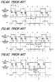
- This invention relates to an FM (frequency-modulation) multiplex decoder circuit, and more particularly to, an FM multiplex decoder circuit equipped with a correction circuit for correcting a bit deviation caused by a variation of cycle in detection signal.
- FM multiplex broadcast that, in addition to conventional stereophonic sound broadcast, digital data such as traffic information, weather forecast etc. are multiplexed has been started.
- FM composite signal S1 is signal that audio signal and digital data, which is composed of block identification code (BIC) and where one block is of 272 bits, are frequency-modulated.
- Block identification code (BIC) "0" corresponds to 72 kHz and BIG "1" corresponds to 80 kHz.
- FM composite signal S1 is converted from analogue value to digital value by an A/D converter 91, then input to a bandpass filter 92 so as to extract block identification code (BIC)
- a detector circuit 93 receives 72 kHz and 80 kHz signal, outputting detection signal S2 to an FM decoder 94.
- detection signal S2 is serial data with a frequency of 16 kHz, it is asynchronous signal including no clock. Therefore, it is necessary to synchronize it by a synchronous processing circuit 95 composing the FM decoder 94 to latch data.
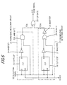
- the synchronous processing circuit 95 comprises an edge detection circuit 101 to output edge signal S4 and a sampling clock generator circuit 102 to which edge signal S4 is input and which generates sampling clock S6 that is clock signal for a latch circuit 103 and a shift register 104.
- the sampling clock generator circuit 102 comprises a 5-bit binary counter 105 to the reset terminal of which edge signal S4 is input, a decoder circuit 106 which decodes output signal S5 of the binary counter 105 and then outputs it to a flip flop 107, and the flip flop 107 which operates with clock signal having a frequency higher than sampling clock S6.
- the edge detection circuit 101 When detection signal S2 rises at time t1 in FIG.3, the edge detection circuit 101 outputs edge signal S4 to the reset terminal of the binary counter 105 synchronizing with the rising edge.
- the binary counter 105 is reset and starts counting up every one clock.
- the decoder circuit 106 outputs such decode signal that becomes active when the 5-bit output value of the binary counter 105 is, for example, ten at time t2 after passing T1 second from time t1, to the flip flop 107.
- Time T1 is generally set so that sampling clock S6 locates at the middle of the interval from the rising edge to the falling edge of detection signal S2.
- the flip flop 107 latches decode signal, outputting sampling clock S6 to the latch circuit 103 and the shift register 104. By this method, sampling clock S6 with a constant cycle of T1 is generated.
- detection signal S2 is detected, and then, by using this signal as a trigger, sampling clock S6 to latch data at the middle of 16 kHz is generated. Also, for signal to repeat "1" or “0” continuously, data is latched using 16 kHz-cycle sampling clock on the basis of the first-generated sampling clock S6. So, even when detection signal S2 repeats "1" or "0" continuously, data is taken stably.
- FIG.4B shows an example that bits more than proper multiplex signal are taken. Since time T3 from the rising edge of sampling clock S6 to the rising edge of detection signal S2 is longer than time T1, erroneous extra pulse signal S6a occurs in clock S6. By the rising edge of this pulse signal S6a, "0" in detection signal S2 is latched and extra data "0" occurs in output signal S7.
- FIG.4C shows an example that one-bit data is lost from the proper multiplex signal. Since time T4 from the rising edge of sampling clock S6 to the rising edge of detection signal S2 is shorter than time T1, data "0" to be latched at time t3 properly is lost.
- the saving of received data is conducted by using the error detection and error correction functions.
- the effect of the error detection and error correction functions cannot be brought out, therefore one-block data of 288 bits is lost.
- PN decoding differential decoding
- BIC block identification code
- sampling clock to take detection signal S2 latches data at the middle of 16 kHz data.
- detection signal with a data rate of lower than 31.25 ⁇ S data cannot be taken accurately.
- detection signal S2 incurs a duty error of 3.29 ⁇ S.
- an FM multiplex decoder circuit comprises:
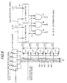
- FIG.5 is a block diagram showing an FM multiplex decoder circuit in the embodiment.
- the FM multiplex decoder circuit comprises an edge detection circuit 11 which detects the rising edge and falling edge of detection signal S2 and generates edge signal S10 corresponding to both the edges, a latch clock generator circuit 12 to which edge signal S10 is input and which outputs latch clock S11, shift clock signal S12, latch clock rise detection signal S11u and latch clock fall detection signal Slid, a latch circuit 13 which latches detection signal S2 synchronizing with latch clock S11 and outputs latch signal S16, an edge interval measurement and comparator circuit 16 to which latch clock rise detection signal S11u, latch clock fall detection signal S11d and 304 kHz clock signal ⁇ (304K) are input and which measures edge interval signal Sedg, determines whether edge interval signal Sedg is between two threshold values m, n (m ⁇ n), smaller than threshold value m or larger than threshold value n, and outputs determination signal SA, SB or SC as the determination result and 5-bit signal SD (SD
- the edge detection circuit 11 is explained below.
- the edge detection circuit 11 comprises a rising edge detection circuit 21 which detects the rising edge of detection signal S2 and then outputs rising edge detection signal S2u to an OR gate 201, a falling edge detection circuit 22 which detects the falling edge of detection signal S2 and then outputs falling edge detection signal S2d to the OR gate 201, and the OR gate 201 which conducts the logical add operation between rising edge detection signal S2u and falling edge detection signal S2d, and outputs edge signal S10.
- the rising edge detection circuit 21 comprises a flip flop 23 to which detection signal S2 is input and which latches detection signal S2 at the rise of basic clock ⁇ which is sufficiently faster than clock signal ⁇ (304K), an inverter 24 which inverts output of the flip flop 23, and an AND gate 25 which conducts the logical product operation between detection signal S2 and output of the inverter 24 and then outputs rising edge detection signal S2u to the OR gate 201.
- the flip flops used in this embodiment are explained as a device to take input data synchronizing with the rise of clock signal.
- the falling edge detection circuit 22 comprises a flip flop 26 to which detection signal S2 is input and which uses basic clock ⁇ as a clock, an inverter 26 which inverts output of the flip flop 26, an OR gate 28 which conducts the logical add operation between detection signal S2 and output of the inverter 26, and an inverter 29 which inverts output of the OR gate 28 and then outputs falling edge detection signal S2d to the OR gate 201.
- the latch clock generator circuit 12 comprises a 5-bit-composed 19 counter 31 to the reset terminal of which edge signal S10 is input and which counts in a base-19 number system using clock signal ⁇ (304K), an AND gate 32 which conducts the logical product operation of 5-bit outputs of the 19 counter 31, a flip flop 33 to which output of the AND gate 32 is input and which uses clock signal ⁇ (304K) as a clock, a flip flop 34 to which output of the flip flop 33 is input and which outputs latch clock S11, a rising edge detection signal 35 which detects the rising edge of output signal of the flip flop 33 and then generates latch clock rise detection signal S11u with a narrow pulse width synchronizing with the rising edge, and a falling edge detection signal 36 which detects the falling edge of output signal of the flip flop 33 and then generates latch clock fall detection signal S11d with a narrow pulse width synchronizing with the falling edge.
- the 19 counter 31 which is reset by edge signal S10 input to the reset terminal R, counts up one by one every time clock signal ⁇ (304K) is input, and returns to "0" when counting up by one from 18.
- the AND gate 32 decodes output of the 19 counter 31 to output "1" at a timing corresponding to time T2 in FIGS.4A-4C. In other words, it operates so that "1" generates at the middle of pulse width T1 in FIGS.4A-4C.
- the flip flop 33 takes output signal of the AND gate 32 with clock signal ⁇ (304K), and outputs it as clock shift signal S12. Also, the flip flop 34 takes clock shift signal S12 with clock signal ⁇ (304K), and outputs latch clock S11.
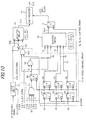
- the edge interval measurement and comparator circuit 16 comprises a 5-bit counter 41 to the rest terminal R of which latch clock fall detection signal S11d is input and which outputs 5-bit output signal SD4 to SD0 with clock signal ⁇ (304K), flip flops 421 to 425 which take output SD4 to SD0 of the 5-bit counter 41 with latch clock rise detection signal S11u, 5-bit comparators 43, 44 which compare whether 5-bit data from the flip flops 421 to 425 is larger than threshold values m and n, respectively, or not, and AND gates 45 to 47.
- edge interval measurement and comparator circuit 16 The operation of the edge interval measurement and comparator circuit 16 is explained below.
- the 5-bit counter 41 When latch clock fall detection signal S11d is input to the reset terminal R, the 5-bit counter 41 is reset, and starts counting up clock signal ⁇ (304K) and outputs it as output signal SD4 to SD0 to the flip flops 421 to 425.
- the flip flops 421 to 425 take output signal SD4 to SD0 with latch clock rise detection signal S11u. Thus, by using the 5-bit counter 41 and the flip flops 421 to 425, the time interval between latch clock fall detection signal Slid and latch clock rise detection signal S11u is measured.
- the flip flops 421 to 425 outputs 5-bit edge interval signal Sedg as the measurement result to the 5-bit comparators 43, 44.
- the 5-bit comparator 43 compares 5-bit edge interval signal Sedg input to five-input terminal A (A4 to A0) with 5-bit threshold value m (m4 to m0) input to five-input terminal B (B4 to B0) . If Sedg ⁇ m, then “1" is output, and if Sedg>m, then "0" is output.
- the 5-bit comparator 44 compares 5-bit edge interval signal Sedg input to five-input terminal A (A4 to A0) with 5-bit threshold value n (n4 to n0) input to five-input terminal B (B4 to B0). If Sedg ⁇ n, then “1” is output, and if Sedg>n, then "0" is output.
- n is set to be 22 three more than 19. Namely, by the 5-bit comparators 43, 44, it is determined whether edge interval signal Sedg is smaller than 16, between 16 and 22, or larger than 22.
- the AND gates 45 to 47 generate determination signals SA, SB and SC in truth-value table shown in FIG.9 from outputs X and Y of the comparators 43 and 44, respectively.
- the selector control circuit 17 comprises flip flops 61 to 63 to which determination signals SA, SB and SC output from the AND gates 45 to 47 as shown in FIG.8 are input and which use clock signal ⁇ (304K) as a clock, flip flops 64 to 66 to which outputs of the flip flops 61 to 63 are input and which use clock signal ⁇ (304K) as a clock and output control signals Sa, Sb and Sc to the selector circuit 18, an AND gate 67 to which output signal SD (SD4 to SD0) of the 5-bit counter 41 is input, a flip flop 68 to which output of the AND gate 67 is input and which use clock signal ⁇ (304K) as a clock, an OR gate 69 to which output of the flip flop 68 and shift clock signal S12 are input and which outputs signal Sd to the selector circuit 18, and an AND gate 601 to which output of the flip flop 68 and determination signal SC are input.
- the selector circuit 15 selects inverted latch signal S16 (bar) as output signal S17 when "1" is input to terminal S, and selects latch signal S16 when "0" is input terminal S.
- the selector circuit 18 selects "0" input to terminal ⁇ when control signal Sa input to terminal a is "1”, selects shift clock signal S12 input to terminal ⁇ when control signal Sb is “1”, and selects output signal Sd of the OR gate 69 input to terminal ⁇ when control signal Sc is "1".
- control Sb is “1" and the others are "0". Therefore, the selector circuit 18 selects shift clock signal S12, outputting it as output signal S14 to the flip flop 19.
- control signal Sa for control signals Sa, Sb and Sc from the flip flops 64 to 66 in FIG.10, as shown in FIG.11, only control signal Sa is “1" and the others are “0".
- the selector circuit 18 selects "0” and erroneous shift clock signal S12a is forced into stopping, and shift clock S15 is as shown in FIG.11.
- the selector circuit 15 Since output of the AND gate 601 is "0", the selector circuit 15 outputs latch signal S16 unalteredly, as output signal S17, to the shift register 14.
- shift clock S15 is forced into stopping when edge interval signal Sedg decreases, erroneous extra data is not sent to the shift register 14 and data that detection signal S2 is normally decoded is output from the shift register 14.
- control signal Sc is "1" and the others are "0".
- the selector circuit 18 selects output signal Sd from the OR gate 69, outputting it as output signal S14 to the flip flop 19.
- shift clock S15 becomes two continuous pulse signals S15a and S15b which are obtained adding shift clock signal S12 and output signal from the flip flop 68 by the OR gate 69.
- the terminal S of the selector circuit 15 changes like “0" ⁇ "1" ⁇ "0". So, it becomes “1” in a period for shift clock S15a newly generated, therefore inverted latch signal S16 (bar) is selected. Thus, the shift register 14 can take data lost to latch signal S16.
- the shift clock is forced into stopping. Therefore, erroneous extra data is not sent to the shift register, thereby data that detection signal is normally decoded can be output from the shift register.
Landscapes
- Engineering & Computer Science (AREA)
- Signal Processing (AREA)
- Computer Networks & Wireless Communication (AREA)
- Circuits Of Receivers In General (AREA)
- Stereo-Broadcasting Methods (AREA)
- Digital Transmission Methods That Use Modulated Carrier Waves (AREA)
- Synchronisation In Digital Transmission Systems (AREA)
- Dc Digital Transmission (AREA)
Applications Claiming Priority (2)
| Application Number | Priority Date | Filing Date | Title |
|---|---|---|---|
| JP30913698 | 1998-10-29 | ||
| JP30913698A JP3323139B2 (ja) | 1998-10-29 | 1998-10-29 | Fm多重復号回路 |
Publications (2)
| Publication Number | Publication Date |
|---|---|
| EP0998049A2 true EP0998049A2 (fr) | 2000-05-03 |
| EP0998049A3 EP0998049A3 (fr) | 2004-01-28 |
Family
ID=17989343
Family Applications (1)
| Application Number | Title | Priority Date | Filing Date |
|---|---|---|---|
| EP99121579A Withdrawn EP0998049A3 (fr) | 1998-10-29 | 1999-10-29 | Décodeur de signaux multiplexé à modulation de fréquence |
Country Status (2)
| Country | Link |
|---|---|
| EP (1) | EP0998049A3 (fr) |
| JP (1) | JP3323139B2 (fr) |
Family Cites Families (2)
| Publication number | Priority date | Publication date | Assignee | Title |
|---|---|---|---|---|
| JP3248382B2 (ja) * | 1995-02-08 | 2002-01-21 | 神鋼電機株式会社 | Fmデコーダ |
| JP3424379B2 (ja) * | 1995-03-30 | 2003-07-07 | カシオ計算機株式会社 | 選択呼出受信装置 |
-
1998
- 1998-10-29 JP JP30913698A patent/JP3323139B2/ja not_active Expired - Fee Related
-
1999
- 1999-10-29 EP EP99121579A patent/EP0998049A3/fr not_active Withdrawn
Also Published As
| Publication number | Publication date |
|---|---|
| JP3323139B2 (ja) | 2002-09-09 |
| JP2000138720A (ja) | 2000-05-16 |
| EP0998049A3 (fr) | 2004-01-28 |
Similar Documents
| Publication | Publication Date | Title |
|---|---|---|
| GB2243269A (en) | Decoding binary-coded transmissions | |
| JPS6068787A (ja) | フレ−ミングコ−ド検出回路 | |
| US4525848A (en) | Manchester decoder | |
| EP0265080B1 (fr) | Dispositif pour la détection de la difference de bit-phase | |
| US5778031A (en) | Decoding circuit for bi-phase BPSK signal having a high noise immunity | |
| EP0998049A2 (fr) | Décodeur de signaux multiplexé à modulation de fréquence | |
| US4486715A (en) | Frequency shift key demodulator | |
| EP0880248A1 (fr) | Circuit pour la détection d'un signal de synchronisation lors de la transmission de données avec synchronisation de trâme | |
| EP0561570A2 (fr) | Dispositif discriminateur de standard de télévision | |
| US4499425A (en) | Phase velocity sign detector for frequency shift key demodulation | |
| US5510786A (en) | CMI encoder circuit | |
| US5566212A (en) | Phase-locked loop circuit for Manchester-data decoding | |
| GB2284915A (en) | Radio selective calling receiver | |
| US7626451B2 (en) | Data demodulation using an asynchronous clock | |
| US20020118774A1 (en) | All-digital FSK demodulation with selectable data rate and adjustable resolution | |
| JPH0738630B2 (ja) | デジタルパターンデコーダおよびデコード方法 | |
| JPH07114414B2 (ja) | 受信障害種別識別方法 | |
| JPH07202706A (ja) | パルス幅変調信号のディジタル信号への復調回路 | |
| KR970003971B1 (ko) | 위성 방송 수신 시스템에서 동기검출기의 위상 천이 보정 장치 | |
| JPH0531973B2 (fr) | ||
| KR0149720B1 (ko) | 맨체스터 디코더 | |
| JP3397829B2 (ja) | 位相検出回路 | |
| JPS63116537A (ja) | 同期保護回路 | |
| JPS6284687A (ja) | オ−トスライス回路 | |
| JPS62281534A (ja) | フレ−ム同期パタ−ン相関検出回路 |
Legal Events
| Date | Code | Title | Description |
|---|---|---|---|
| PUAI | Public reference made under article 153(3) epc to a published international application that has entered the european phase |
Free format text: ORIGINAL CODE: 0009012 |
|
| AK | Designated contracting states |
Kind code of ref document: A2 Designated state(s): AT BE CH CY DE DK ES FI FR GB GR IE IT LI LU MC NL PT SE |
|
| AX | Request for extension of the european patent |
Free format text: AL;LT;LV;MK;RO;SI |
|
| PUAL | Search report despatched |
Free format text: ORIGINAL CODE: 0009013 |
|
| AK | Designated contracting states |
Kind code of ref document: A3 Designated state(s): AT BE CH CY DE DK ES FI FR GB GR IE IT LI LU MC NL PT SE |
|
| AX | Request for extension of the european patent |
Extension state: AL LT LV MK RO SI |
|
| AKX | Designation fees paid | ||
| REG | Reference to a national code |
Ref country code: DE Ref legal event code: 8566 |
|
| STAA | Information on the status of an ep patent application or granted ep patent |
Free format text: STATUS: THE APPLICATION IS DEEMED TO BE WITHDRAWN |
|
| 18D | Application deemed to be withdrawn |
Effective date: 20040729 |