EP1002647A2 - Procédé et dispositif d'électroformage pour plaque à orifices à jet d'encre - Google Patents
Procédé et dispositif d'électroformage pour plaque à orifices à jet d'encre Download PDFInfo
- Publication number
- EP1002647A2 EP1002647A2 EP99203680A EP99203680A EP1002647A2 EP 1002647 A2 EP1002647 A2 EP 1002647A2 EP 99203680 A EP99203680 A EP 99203680A EP 99203680 A EP99203680 A EP 99203680A EP 1002647 A2 EP1002647 A2 EP 1002647A2
- Authority
- EP
- European Patent Office
- Prior art keywords
- film
- substrate
- nozzle plate
- mandrel
- relief patterns
- Prior art date
- Legal status (The legal status is an assumption and is not a legal conclusion. Google has not performed a legal analysis and makes no representation as to the accuracy of the status listed.)
- Withdrawn
Links
- 238000000034 method Methods 0.000 title claims abstract description 31
- 238000005323 electroforming Methods 0.000 title description 5
- 229910052751 metal Inorganic materials 0.000 claims abstract description 59
- 239000002184 metal Substances 0.000 claims abstract description 59
- 239000000758 substrate Substances 0.000 claims abstract description 50
- 238000004519 manufacturing process Methods 0.000 claims abstract description 18
- 239000012811 non-conductive material Substances 0.000 claims description 6
- 238000000151 deposition Methods 0.000 claims description 5
- 239000000463 material Substances 0.000 claims description 5
- 238000007639 printing Methods 0.000 abstract description 4
- 229920002120 photoresistant polymer Polymers 0.000 description 20
- 238000004070 electrodeposition Methods 0.000 description 13
- VYPSYNLAJGMNEJ-UHFFFAOYSA-N Silicium dioxide Chemical compound O=[Si]=O VYPSYNLAJGMNEJ-UHFFFAOYSA-N 0.000 description 10
- 230000015572 biosynthetic process Effects 0.000 description 6
- 235000012239 silicon dioxide Nutrition 0.000 description 5
- 239000000377 silicon dioxide Substances 0.000 description 5
- PXHVJJICTQNCMI-UHFFFAOYSA-N Nickel Chemical compound [Ni] PXHVJJICTQNCMI-UHFFFAOYSA-N 0.000 description 4
- 238000009713 electroplating Methods 0.000 description 4
- 239000011521 glass Substances 0.000 description 4
- 238000007641 inkjet printing Methods 0.000 description 4
- 239000003989 dielectric material Substances 0.000 description 3
- 238000005530 etching Methods 0.000 description 3
- VYZAMTAEIAYCRO-UHFFFAOYSA-N Chromium Chemical compound [Cr] VYZAMTAEIAYCRO-UHFFFAOYSA-N 0.000 description 2
- 229910052804 chromium Inorganic materials 0.000 description 2
- 239000011651 chromium Substances 0.000 description 2
- 239000004020 conductor Substances 0.000 description 2
- 239000013078 crystal Substances 0.000 description 2
- 238000005516 engineering process Methods 0.000 description 2
- 229910052759 nickel Inorganic materials 0.000 description 2
- 230000002159 abnormal effect Effects 0.000 description 1
- 230000008021 deposition Effects 0.000 description 1
- 238000005137 deposition process Methods 0.000 description 1
- 230000000694 effects Effects 0.000 description 1
- 230000001788 irregular Effects 0.000 description 1
- 230000007246 mechanism Effects 0.000 description 1
- 238000000059 patterning Methods 0.000 description 1
- 238000003908 quality control method Methods 0.000 description 1
- 238000007493 shaping process Methods 0.000 description 1
- 239000007787 solid Substances 0.000 description 1
- XLYOFNOQVPJJNP-UHFFFAOYSA-N water Substances O XLYOFNOQVPJJNP-UHFFFAOYSA-N 0.000 description 1
Images


Classifications
-
- B—PERFORMING OPERATIONS; TRANSPORTING
- B41—PRINTING; LINING MACHINES; TYPEWRITERS; STAMPS
- B41J—TYPEWRITERS; SELECTIVE PRINTING MECHANISMS, i.e. MECHANISMS PRINTING OTHERWISE THAN FROM A FORME; CORRECTION OF TYPOGRAPHICAL ERRORS
- B41J2/00—Typewriters or selective printing mechanisms characterised by the printing or marking process for which they are designed
- B41J2/005—Typewriters or selective printing mechanisms characterised by the printing or marking process for which they are designed characterised by bringing liquid or particles selectively into contact with a printing material
- B41J2/01—Ink jet
- B41J2/135—Nozzles
- B41J2/16—Production of nozzles
- B41J2/1621—Manufacturing processes
- B41J2/1625—Manufacturing processes electroforming
-
- B—PERFORMING OPERATIONS; TRANSPORTING
- B41—PRINTING; LINING MACHINES; TYPEWRITERS; STAMPS
- B41J—TYPEWRITERS; SELECTIVE PRINTING MECHANISMS, i.e. MECHANISMS PRINTING OTHERWISE THAN FROM A FORME; CORRECTION OF TYPOGRAPHICAL ERRORS
- B41J2/00—Typewriters or selective printing mechanisms characterised by the printing or marking process for which they are designed
- B41J2/005—Typewriters or selective printing mechanisms characterised by the printing or marking process for which they are designed characterised by bringing liquid or particles selectively into contact with a printing material
- B41J2/01—Ink jet
- B41J2/135—Nozzles
- B41J2/16—Production of nozzles
- B41J2/162—Manufacturing of the nozzle plates
Definitions
- This invention relates to a method and mandrel for the electroforming of nozzle plates for an inkjet printer.
- Inkjet printing has become a prominent contender in the digital output arena because of its nonimpact, low-noise characteristics, and its compatibility with plain paper. Ink jet printing avoids the complications of toner transfers and fixing required in electrophotography, and the pressure contact at the printing interface required in thermal resistive printing technologies.
- ink jet printing mechanisms including continuous ink jet printers or drop-on-demand printers. This application is principally concerned with the nozzle plates necessary to carry out drop-on-demand type ink jet printing. However, before the significance of the invention can be appreciated, some background on drop-on-demand printing is necessary.
- Patent 3,946,398 discloses a drop-on-demand ink jet printer which applies a high voltage to a piezoelectric crystal, causing the crystal to bend and to apply pressure on an ink reservoir, thereby squeezing drops on demand through the small openings in the nozzle plate of the printer.
- Other examples of piezoelectric ink jet printers are disclosed in EP 827 833 A2 and WO 98/08687.
- British Patent 2,007,162 discloses an electrothermal drop-on-demand ink jet printer which applies a power pulse to an electrothermal heater which is in thermal contact with water based ink in a nozzle.
- Ink nozzles are an essential component in all such drop-on-demand ink jet printers.
- the shape and dimension of an ink nozzle determine the size and trajectory of the ink drop ejected from it. If the diameter of the ink nozzle opening deviates from the desired size, both ink drop volume and the velocity can vary from the desired values. If the opening of an ink nozzle has an irregular, non-circular shape, the direction of the ejected ink drop from the ink nozzle can also deviate from the desired direction which is usually normal to the plane of the nozzle plate. As velocity and direction determine trajectory, an abnormal variation in either can result in the ink drop missing its desired target.
- Ink jet nozzle plates are often formed by an electroforming process.
- a mandrel is formed by overcoating a substrate with a conductive film.
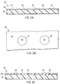
- FIGs 1A-1C illustrate a substrate 1 formed from silicon dioxide (or other nonconductive material) that has been overcoated with a conductive film 3 of a metal, such as chromium or nickel.
- a photoresist 5 (shown in phantom in Figure 1A) is then applied to the conductive film 3, imaged, and developed to expose selected areas 7 of the film 3.
- These selected areas 7 of the conductive film 3 are removed by exposing the film to an etchant, leaving a relief pattern 9, and completing the formation of the mandrel 10 for the nozzle plate.
- the selected areas removed from the conductive film are circular holes 9, each corresponding to an ink nozzle to be formed.
- the mandrel 10 formed by this process is shown in Figures 1B and 1C.
- a metallic nozzle plate 12 (shown in phantom) is formed using the mandrel 10 by electroplating a layer of metal 13 over the conductive film. Initially, the metal layer 13 covers only the metallic film 3. Over time, the metallic layer 13 grows in thickness and develops a growth front 14 that closes over the circular holes 9 where the conductive film 3 was removed.
- a nozzle exit opening 16 is defined by the edge of the growth front 14 of the metallic layer 13 on top of the substrate 1. The nozzle exit diameter is defined by controlling the electroplating time for a given set of electroplating conditions.
- Ink nozzle plates can also be formed in an electroforming process by a mandrel having positive relief patterns, such as disks, as opposed to the mandrel 10 having negative relief patterns in the form of circular holes 9.
- the applicants have experienced several problems in using in the above-described prior art to manufacture nozzle plates.
- the most serious of these problems is variability of the diameter of the ink nozzles.
- the growth rate of the metallic layer can vary at different areas of the mandrel in the electroforming process as well as between different batches.
- the growth rate variability results in variability in the size of the openings as defined by the edge of the growth front of the metallic layer. This problem is particularly severe for forming ink nozzles with small diameters.
- a slight variability in the growth rate of the metallic layer the in electroplating process will result in a large relative error in the nozzle diameter.
- Other problems include the fact that the nozzle exits are sometimes formed off-center or in an off-circular shape due to uneven advancement of the metal layer growth front.
- An object of the invention is to provide a method and a mandrel for manufacturing a nozzle plate that overcomes or at least ameliorates all of the aforementioned problems.
- a method of the invention includes the steps of providing a substrate, depositing a film over the substrate having a plurality of relief patterns, and providing a post structure on a top center portion of at least some of the relief patterns to form a mandrel, each of which has a width less than the width of the relief pattern.
- the vertical height of each post structure is no greater than the vertical height of the pattern, whether the pattern is formed from negative relief (such as a circular hole) or positive relief (such as a disk-shaped "island" of dielectric).
- Such dimensioning advantageously results in funnel-shaped nozzles having discharge openings with precisely dimensioned diameters.
- metal is deposited over the mandrel created by the aforementioned steps until the metal layer is formed having openings with a width defined by the width of post structures.
- the metal layer is preferably electrodeposited over the film covering the substrate until a growth front of an electrodeposited metal layer first contacts the post structure, whereupon the electrodepositing step is terminated.
- the deposited layer of metal is then released from the mandrel formed by the film in the substrate to create the finished nozzle plate.
- each of the post structures has a bottom end attached to the substrate, a flank portion surrounded by side walls of one of the holes in the film, and a top end that extends above a top surface of the film a vertical distance that is less than a vertical height of the side walls.
- the substrate is preferably formed from a nonconductive material, such a silicon dioxide, and the film is provided by depositing a layer of metal over the substrate, and the relief patterns are formed from a plurality of uniformly spaced and diametered circular holes formed by a combination of photolithographic and etching techniques.
- the post structures are formed in the centers of each of the circular holes by the deposition of a dielectric, followed by photoresistive patterning and etching. Alternatively, the center diametric post structures can be patterned directly from photoresist materials.
- the flanks of the post structures are preferably cylindrical in shape in order to impart circular openings in the nozzles that they ultimately form in the nozzle plate.
- the substrate is preferably formed from an electrically conductive material, such as metal, while the film is an electrically-nonconductive layer which may be formed from photoresist or a dielectric such as silicon dioxide.
- the disk-shaped patterns in the film are preferably formed by known photolithographic and etching techniques.
- the post structures are formed in the centers of the resulting disk from electrically nonconductive materials in the same manner that the patterns are created in the first nonconductive film, i.e., via a layer of photoresist or silicon dioxide that has been photolithographically patterned and etched.
- each of the post structures has a bottom end attached to one of the disk-shaped film "islands," a top end, and a vertical height between the top and bottom ends that is less than a vertical height of the side walls of the film "island" upon which it sits.
- a layer of metal is deposited preferably via electrodeposition techniques over the mandrel created by the substrate, film release structures, and post structures.
- the metal in layer begins to build over the edges of the relief structures and close in around the post structures.
- the electrodeposition step is terminated.
- the electrodeposited metal layer is then separated from the mandrel, resulting in a nozzle plate having nozzles that are extremely uniform in dimensioning and ink discharge characteristics.
- the first embodiment 20 of the invention is formed from a nonconductive substrate 22, which may be, for example, glass.
- a conductive film 24, which may be a metal such as chromium or nickel, is deposited over the top surface of the substrate 22 in a continuous layer of uniform thickness which may be as thin as 1000A or thicker if desired.
- a layer of photoresist 26 is then applied over the top surface of the conductive metal film 24. The photoresist 26 is patterned and developed to expose selected areas 28 of the conductive metal film 24, as is indicated in phantom in Figure 2A.
- the selected areas 28 are circular so that a relief pattern in the form of circular holes 30 is formed when the selected areas 28 of the conductive metal film 24 are exposed to either a wet or a dry etchant.
- the resulting circular holes 30 extend through the conductive metal film 24 to the upper surface of the substrate 22 as indicated in Figures 2B and 2C.
- the circular holes 30 may also be formed by a "lift-off" process known in the prior art. In this process, a photoresist is first applied and developed in circular patterns on the top surface of the substrate before the conductive metal film 24 is applied. The film 24 is then applied over the substrate 22 at all points including the circular patterns of photoresist. The photoresist is then removed taking with it the conductive metal film 24 applied over it, resulting in a conductive metal film 24 having circular holes 30.
- the upper surface of the conductive metal film 24 is overcoated with another layer of photoresist 32, as is indicated in Figure 2C. Cylindrical areas 33 of the photoresist layer 32 are selectively exposed in accordance with known photolithographic techniques.
- the photoresist layer 32 is then developed, leaving a cylindrically-shaped post member 34 connected to the upper surface of the glass substrate 22 and concentrically disposed within each of the circular holes 30 in the conductive metal film 24. This structure is illustrated in Figure 2D.
- the development of the photoresist layer 32 in this manner creates a mandrel 35 which may be advantageously used to form the ink jet nozzle plate of the invention.
- the cylindrical flanks 36 of each of the post members 34 have very nearly the same diameter D1 (as indicated in Figure 2E).
- the diameter D1 of each of the post members 34 can be controlled to within 1 micron.
- the uniformity of the diameter D1 throughout all of the nozzle making areas formed by the circular holes 30 results in extremely uniform nozzle diameters.
- the absolute height of the post members 34 can vary between several thousand Angstroms to tens of microns. As will become more evident hereinafter, such dimensioning advantageously results in a funnel-shaped profile for each of the nozzles formed in the resulting nozzle plate.
- the thickness of the photoresist layer 32 is selected so that the height of the resulting post members 34 above the top surface of the photoresist layer 32 is preferably equal to or less than the height of the side walls of the circular holes 30.
- the height H1 of each of the post members 34 over the top surface of the conductive metal film 24 is preferably no more than the height H2 of the walls of the circular hole 30 that the post member 34 resides.
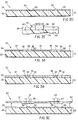
- An ink jet nozzle plate is formed by the gradual electrodeposition of a metal layer 37 over the top face of the mandrel 35.
- Figures 3A, 3B, and 3C illustrate how the mandrel 35 of the invention is used to form an ink jet nozzle plate.
- a metal layer 37 is gradually electrodeposited over the upper surface of the mandrel 35.
- Metal layer 37 first covers the upper surface of the conductive metal layer 24.
- a front 38 of eletrodeposited metal grows over the side walls of the circular holes 30 in the conductive metal film 24. As the metal layer 37 thickens over time, these growth fronts 38 (which are funnel-shaped perspectives) converge toward the cylindrical flanks 36 of the post members 34.
- an ink jet nozzle plate 40 is formed by separating the metal layer 37 from the mandrel 35.
- the nozzle exit diameter of each of the nozzles formed on the plate 40 has an inner diameter D2 which is essentially identical to the outer diameter D1 of the post member that helped to form it.
- each of the discharge throats 44 is advantageously funnel-shaped, diverging almost immediately from the bottom side of the nozzle plate 40 to its top side.
- Such a divergent funnel shape advantageously provides a sharp "pinch point" for droplets of ink to accurately and consistently form when pressurized ink is discharged through the discharge throats 44.
- Figures 4A, 4B, 4C, and 4D illustrate the fabrication of an alternate embodiment 50 of the mandrel of the invention.
- a conductive substrate 52 is used in lieu of a nonconductive substrate formed from glass or other dielectric material. While the substrate 52 in this example is illustrated as being formed from solid metal, substrate 52 may also be formed from a dielectric layer of material (such as glass) that has been overcoated with a layer of conductive material. In either form, the conductive substrate 52 is next covered with a film of electrically nonconductive material, such as silicon dioxide.
- a first layer of photoresist is applied over the top surface of the nonconductive film 54 and patterned via standard photolithographic techniques to cover all but a plurality of selected, circular areas 58.
- the resulting laminated structure is then exposed to either a dry or wet etchant to remove the exposed areas of the nonconductive film 54, which has the effect of producing a plurality of uniformly diametered disk-shaped islands 60 of nonconductive film 54 over the top surface of the conductive substrate 52 as shown in Figure 4B.
- the laminated structure of Figure 4B is then covered with a layer 62 of a photoresistive material, which is exposed in post areas 64 and then developed to leave a cylindrical post member 66 concentrically disposed at the center of each of the disk-shaped islands 60 of dielectric material.
- the resulting laminated structure forms the mandrel 70 shown in Figure 4D which forms a second embodiment of the invention, and which may also be used to advantageously form an inkjet nozzle plate having nozzles of extremely uniform dimensions.
- the height H3 of the post members 66 is no more than equal to, and is preferably less than the height H4 of the side walls of the disk-shaped islands 60 of dielectric.
- Figure 5A illustrates the first step in the formation of an ink jet nozzle plate over the mandrel 70.
- a metal layer 72 is deposited over the top surface of the mandrel 70.
- the metal layer 72 covers the exposed metal surface of the substrate 52.
- the growth front 74 of the metal layer 72 spills over onto the disk-shaped islands 60 of dielectric, as shown in Figure 5A.
- the electrodeposition of metal continues, the metal layer 72 becomes thicker, and the growth fronts 74 converge in a funnel-shape until they finally contact the cylindrical flanks of the post members 66 as shown in Figure 5B. At this juncture, the electrodeposition step is terminated.
- the metal layer 72 is separated from the upper surface of the mandrel 70, creating an ink jet plate 75 having funnel-shaped discharge throats 78 having an inner diameter D4 which is very nearly the same as the outer diameter D3 of the post members 66.
- the invention has been described in the context of the manufacture of an ink jet nozzle plate, the invention may be advantageously used to form any type of small diametered orifice for any application.
- the resulting nozzle plate has been described as an electrodeposited metal plate, the plate may be by other types of deposition processes, and may be formed from a non-metallic, dielectric material.
Landscapes
- Engineering & Computer Science (AREA)
- Manufacturing & Machinery (AREA)
- Particle Formation And Scattering Control In Inkjet Printers (AREA)
Applications Claiming Priority (2)
| Application Number | Priority Date | Filing Date | Title |
|---|---|---|---|
| US19327698A | 1998-11-17 | 1998-11-17 | |
| US193276 | 1998-11-17 |
Publications (2)
| Publication Number | Publication Date |
|---|---|
| EP1002647A2 true EP1002647A2 (fr) | 2000-05-24 |
| EP1002647A3 EP1002647A3 (fr) | 2001-02-21 |
Family
ID=22712951
Family Applications (1)
| Application Number | Title | Priority Date | Filing Date |
|---|---|---|---|
| EP99203680A Withdrawn EP1002647A3 (fr) | 1998-11-17 | 1999-11-05 | Procédé et dispositif d'électroformage pour plaque à orifices à jet d'encre |
Country Status (2)
| Country | Link |
|---|---|
| EP (1) | EP1002647A3 (fr) |
| JP (1) | JP2000168093A (fr) |
Cited By (1)
| Publication number | Priority date | Publication date | Assignee | Title |
|---|---|---|---|---|
| CN103203958A (zh) * | 2012-01-16 | 2013-07-17 | 昆山允升吉光电科技有限公司 | 一种电铸模板的制作工艺 |
Citations (5)
| Publication number | Priority date | Publication date | Assignee | Title |
|---|---|---|---|---|
| US3946398A (en) | 1970-06-29 | 1976-03-23 | Silonics, Inc. | Method and apparatus for recording with writing fluids and drop projection means therefor |
| GB2007162A (en) | 1977-10-03 | 1979-05-16 | Canon Kk | Liquid jet recording process and apparatus therefor |
| US4460728A (en) | 1983-02-28 | 1984-07-17 | National Starch And Chemical Corporation | Hot melt adhesive compositions |
| WO1998008687A1 (fr) | 1996-08-27 | 1998-03-05 | Topaz Technologies, Inc. | Tete d'impression a jet d'encre produisant des gouttelettes d'encre de volume variable |
| EP0827833A2 (fr) | 1996-08-27 | 1998-03-11 | Topaz Technologies, Inc. | Dispositif de tête à jet d'encre |
Family Cites Families (2)
| Publication number | Priority date | Publication date | Assignee | Title |
|---|---|---|---|---|
| US4675083A (en) * | 1986-04-02 | 1987-06-23 | Hewlett-Packard Company | Compound bore nozzle for ink jet printhead and method of manufacture |
| US5560837A (en) * | 1994-11-08 | 1996-10-01 | Hewlett-Packard Company | Method of making ink-jet component |
-
1999
- 1999-11-05 EP EP99203680A patent/EP1002647A3/fr not_active Withdrawn
- 1999-11-08 JP JP31720299A patent/JP2000168093A/ja active Pending
Patent Citations (5)
| Publication number | Priority date | Publication date | Assignee | Title |
|---|---|---|---|---|
| US3946398A (en) | 1970-06-29 | 1976-03-23 | Silonics, Inc. | Method and apparatus for recording with writing fluids and drop projection means therefor |
| GB2007162A (en) | 1977-10-03 | 1979-05-16 | Canon Kk | Liquid jet recording process and apparatus therefor |
| US4460728A (en) | 1983-02-28 | 1984-07-17 | National Starch And Chemical Corporation | Hot melt adhesive compositions |
| WO1998008687A1 (fr) | 1996-08-27 | 1998-03-05 | Topaz Technologies, Inc. | Tete d'impression a jet d'encre produisant des gouttelettes d'encre de volume variable |
| EP0827833A2 (fr) | 1996-08-27 | 1998-03-11 | Topaz Technologies, Inc. | Dispositif de tête à jet d'encre |
Cited By (1)
| Publication number | Priority date | Publication date | Assignee | Title |
|---|---|---|---|---|
| CN103203958A (zh) * | 2012-01-16 | 2013-07-17 | 昆山允升吉光电科技有限公司 | 一种电铸模板的制作工艺 |
Also Published As
| Publication number | Publication date |
|---|---|
| JP2000168093A (ja) | 2000-06-20 |
| EP1002647A3 (fr) | 2001-02-21 |
Similar Documents
| Publication | Publication Date | Title |
|---|---|---|
| US4954225A (en) | Method for making nozzle plates | |
| EP0489246B1 (fr) | Procédé de fabrication de plaques à trois dimensions avec orifices en forme de buses | |
| EP0629504B1 (fr) | Plaque d'orifice pour imprimante à jet d'encre | |
| US4770740A (en) | Method of manufacturing valve element for use in an ink-jet printer head | |
| EP0485182B1 (fr) | Tête d'impression à couche mince thermique à jet d'encre ayant une plaque à tuyères plastique et son procédé de fabrication | |
| EP1027993A1 (fr) | Mandrin pour former une plaque à buses avec surface de non-mouillabilité d'épaisseur uniforme et des buses à contour aminci, et procédé de fabrication de ce mandrin | |
| US6303042B1 (en) | Making ink jet nozzle plates | |
| US6214245B1 (en) | Forming-ink jet nozzle plate layer on a base | |
| US7543915B2 (en) | Fluid ejection device | |
| JPH04276091A (ja) | 連続電鋳方法 | |
| US6022752A (en) | Mandrel for forming a nozzle plate having orifices of precise size and location and method of making the mandrel | |
| WO1987007217A1 (fr) | Tete d'ecriture a l'encre avec membrane a excitation piezoelectrique | |
| US6238584B1 (en) | Method of forming ink jet nozzle plates | |
| US6214192B1 (en) | Fabricating ink jet nozzle plate | |
| US6258286B1 (en) | Making ink jet nozzle plates using bore liners | |
| CN100522622C (zh) | 用于孔板电铸成型的型芯的制造方法及所述型芯 | |
| EP1002647A2 (fr) | Procédé et dispositif d'électroformage pour plaque à orifices à jet d'encre | |
| US7437820B2 (en) | Method of manufacturing a charge plate and orifice plate for continuous ink jet printers | |
| EP1740384B1 (fr) | Architecture microfluide | |
| DE3443564A1 (de) | Fluessigkeitsstrahlaufzeichnungskopf | |
| JP3533205B2 (ja) | マイクロ液滴生成装置およびその製造方法 | |
| JP2000211137A (ja) | インクジェットプリントヘッド用アクチュエ―タ | |
| US7552534B2 (en) | Method of manufacturing an integrated orifice plate and electroformed charge plate | |
| JPH1016236A (ja) | インクジェットプリンタヘッド及びその製造方法 | |
| US7540589B2 (en) | Integrated charge and orifice plates for continuous ink jet printers |
Legal Events
| Date | Code | Title | Description |
|---|---|---|---|
| PUAI | Public reference made under article 153(3) epc to a published international application that has entered the european phase |
Free format text: ORIGINAL CODE: 0009012 |
|
| AK | Designated contracting states |
Kind code of ref document: A2 Designated state(s): AT BE CH CY DE DK ES FI FR GB GR IE IT LI LU MC NL PT SE |
|
| AX | Request for extension of the european patent |
Free format text: AL;LT;LV;MK;RO;SI |
|
| PUAL | Search report despatched |
Free format text: ORIGINAL CODE: 0009013 |
|
| AK | Designated contracting states |
Kind code of ref document: A3 Designated state(s): AT BE CH CY DE DK ES FI FR GB GR IE IT LI LU MC NL PT SE |
|
| AX | Request for extension of the european patent |
Free format text: AL;LT;LV;MK;RO;SI |
|
| AKX | Designation fees paid | ||
| REG | Reference to a national code |
Ref country code: DE Ref legal event code: 8566 |
|
| STAA | Information on the status of an ep patent application or granted ep patent |
Free format text: STATUS: THE APPLICATION IS DEEMED TO BE WITHDRAWN |
|
| 18D | Application deemed to be withdrawn |
Effective date: 20010822 |