EP1003199A2 - Composition comprenant des particules inorganiques, film de transfer la comprenant et procédé de production pour les écrans au plasma - Google Patents
Composition comprenant des particules inorganiques, film de transfer la comprenant et procédé de production pour les écrans au plasma Download PDFInfo
- Publication number
- EP1003199A2 EP1003199A2 EP99119469A EP99119469A EP1003199A2 EP 1003199 A2 EP1003199 A2 EP 1003199A2 EP 99119469 A EP99119469 A EP 99119469A EP 99119469 A EP99119469 A EP 99119469A EP 1003199 A2 EP1003199 A2 EP 1003199A2
- Authority
- EP
- European Patent Office
- Prior art keywords
- film
- material layer
- forming material
- film forming
- resist
- Prior art date
- Legal status (The legal status is an assumption and is not a legal conclusion. Google has not performed a legal analysis and makes no representation as to the accuracy of the status listed.)
- Granted
Links
- 239000000203 mixture Substances 0.000 title claims abstract description 126
- 238000012546 transfer Methods 0.000 title claims abstract description 121
- 239000010954 inorganic particle Substances 0.000 title claims abstract description 60
- 238000004519 manufacturing process Methods 0.000 title claims abstract description 33
- 239000011347 resin Substances 0.000 claims abstract description 35
- 229920005989 resin Polymers 0.000 claims abstract description 35
- 239000004014 plasticizer Substances 0.000 claims abstract description 28
- 125000000217 alkyl group Chemical group 0.000 claims abstract description 27
- 239000011230 binding agent Substances 0.000 claims abstract description 27
- 125000004432 carbon atom Chemical group C* 0.000 claims abstract description 22
- 150000001875 compounds Chemical class 0.000 claims abstract description 21
- 125000003342 alkenyl group Chemical group 0.000 claims abstract description 15
- 125000004450 alkenylene group Chemical group 0.000 claims abstract description 7
- 125000002947 alkylene group Chemical group 0.000 claims abstract description 7
- 239000000463 material Substances 0.000 claims description 237
- 239000000758 substrate Substances 0.000 claims description 98
- -1 acrylate compound Chemical class 0.000 claims description 34
- 238000005530 etching Methods 0.000 claims description 34
- 230000004888 barrier function Effects 0.000 claims description 33
- 239000000470 constituent Substances 0.000 claims description 28
- 239000005001 laminate film Substances 0.000 claims description 16
- 239000004925 Acrylic resin Substances 0.000 claims description 14
- 229920000178 Acrylic resin Polymers 0.000 claims description 14
- 239000011159 matrix material Substances 0.000 claims description 14
- OAICVXFJPJFONN-UHFFFAOYSA-N Phosphorus Chemical compound [P] OAICVXFJPJFONN-UHFFFAOYSA-N 0.000 claims description 13
- 150000001252 acrylic acid derivatives Chemical class 0.000 claims description 11
- 239000006087 Silane Coupling Agent Substances 0.000 claims description 8
- 229920001577 copolymer Polymers 0.000 claims description 8
- 239000000178 monomer Substances 0.000 claims description 5
- 239000002245 particle Substances 0.000 claims description 4
- 229910052804 chromium Inorganic materials 0.000 claims description 3
- 125000002496 methyl group Chemical group [H]C([H])([H])* 0.000 claims description 3
- 229920000642 polymer Polymers 0.000 claims description 3
- 229910001252 Pd alloy Inorganic materials 0.000 claims description 2
- 229910052782 aluminium Inorganic materials 0.000 claims description 2
- 229910052802 copper Inorganic materials 0.000 claims description 2
- 229910052737 gold Inorganic materials 0.000 claims description 2
- 229920001519 homopolymer Polymers 0.000 claims description 2
- 125000004435 hydrogen atom Chemical group [H]* 0.000 claims description 2
- 229910052759 nickel Inorganic materials 0.000 claims description 2
- 125000000962 organic group Chemical group 0.000 claims description 2
- 229910052709 silver Inorganic materials 0.000 claims description 2
- 238000009313 farming Methods 0.000 claims 1
- 239000010408 film Substances 0.000 description 442
- 239000011521 glass Substances 0.000 description 96
- NIXOWILDQLNWCW-UHFFFAOYSA-M Acrylate Chemical compound [O-]C(=O)C=C NIXOWILDQLNWCW-UHFFFAOYSA-M 0.000 description 60
- 239000002585 base Substances 0.000 description 40
- 238000000034 method Methods 0.000 description 38
- 238000000576 coating method Methods 0.000 description 33
- 239000011248 coating agent Substances 0.000 description 30
- 238000010438 heat treatment Methods 0.000 description 21
- 239000002904 solvent Substances 0.000 description 20
- 239000013039 cover film Substances 0.000 description 18
- 229920006395 saturated elastomer Polymers 0.000 description 18
- 239000000843 powder Substances 0.000 description 13
- LYCAIKOWRPUZTN-UHFFFAOYSA-N Ethylene glycol Chemical compound OCCO LYCAIKOWRPUZTN-UHFFFAOYSA-N 0.000 description 12
- 238000001035 drying Methods 0.000 description 10
- 230000008569 process Effects 0.000 description 9
- 238000002834 transmittance Methods 0.000 description 9
- 238000007650 screen-printing Methods 0.000 description 8
- 239000000126 substance Substances 0.000 description 8
- 238000005336 cracking Methods 0.000 description 7
- 239000000243 solution Substances 0.000 description 7
- KWYUFKZDYYNOTN-UHFFFAOYSA-M Potassium hydroxide Chemical compound [OH-].[K+] KWYUFKZDYYNOTN-UHFFFAOYSA-M 0.000 description 6
- ZXPDYFSTVHQQOI-UHFFFAOYSA-N diethoxysilane Chemical class CCO[SiH2]OCC ZXPDYFSTVHQQOI-UHFFFAOYSA-N 0.000 description 6
- YQGOWXYZDLJBFL-UHFFFAOYSA-N dimethoxysilane Chemical class CO[SiH2]OC YQGOWXYZDLJBFL-UHFFFAOYSA-N 0.000 description 6
- SACPKRUZWRIEBW-UHFFFAOYSA-N dipropoxysilane Chemical class CCCO[SiH2]OCCC SACPKRUZWRIEBW-UHFFFAOYSA-N 0.000 description 6
- CWAFVXWRGIEBPL-UHFFFAOYSA-N ethoxysilane Chemical class CCO[SiH3] CWAFVXWRGIEBPL-UHFFFAOYSA-N 0.000 description 6
- 238000011156 evaluation Methods 0.000 description 6
- WGCNASOHLSPBMP-UHFFFAOYSA-N hydroxyacetaldehyde Natural products OCC=O WGCNASOHLSPBMP-UHFFFAOYSA-N 0.000 description 6
- ARYZCSRUUPFYMY-UHFFFAOYSA-N methoxysilane Chemical class CO[SiH3] ARYZCSRUUPFYMY-UHFFFAOYSA-N 0.000 description 6
- 235000011837 pasties Nutrition 0.000 description 6
- ZMYXZXUHYAGGKG-UHFFFAOYSA-N propoxysilane Chemical class CCCO[SiH3] ZMYXZXUHYAGGKG-UHFFFAOYSA-N 0.000 description 6
- 230000005855 radiation Effects 0.000 description 6
- VYPSYNLAJGMNEJ-UHFFFAOYSA-N Silicium dioxide Chemical compound O=[Si]=O VYPSYNLAJGMNEJ-UHFFFAOYSA-N 0.000 description 5
- 230000015572 biosynthetic process Effects 0.000 description 5
- 229910052810 boron oxide Inorganic materials 0.000 description 5
- JKWMSGQKBLHBQQ-UHFFFAOYSA-N diboron trioxide Chemical compound O=BOB=O JKWMSGQKBLHBQQ-UHFFFAOYSA-N 0.000 description 5
- 230000000694 effects Effects 0.000 description 5
- 229910052814 silicon oxide Inorganic materials 0.000 description 5
- SOGAXMICEFXMKE-UHFFFAOYSA-N Butylmethacrylate Chemical compound CCCCOC(=O)C(C)=C SOGAXMICEFXMKE-UHFFFAOYSA-N 0.000 description 4
- RTZKZFJDLAIYFH-UHFFFAOYSA-N Diethyl ether Chemical compound CCOCC RTZKZFJDLAIYFH-UHFFFAOYSA-N 0.000 description 4
- PPBRXRYQALVLMV-UHFFFAOYSA-N Styrene Chemical compound C=CC1=CC=CC=C1 PPBRXRYQALVLMV-UHFFFAOYSA-N 0.000 description 4
- XLOMVQKBTHCTTD-UHFFFAOYSA-N Zinc monoxide Chemical compound [Zn]=O XLOMVQKBTHCTTD-UHFFFAOYSA-N 0.000 description 4
- 239000001913 cellulose Substances 0.000 description 4
- 229920002678 cellulose Polymers 0.000 description 4
- 239000002131 composite material Substances 0.000 description 4
- 238000011161 development Methods 0.000 description 4
- 238000004898 kneading Methods 0.000 description 4
- 229910000464 lead oxide Inorganic materials 0.000 description 4
- YEXPOXQUZXUXJW-UHFFFAOYSA-N oxolead Chemical compound [Pb]=O YEXPOXQUZXUXJW-UHFFFAOYSA-N 0.000 description 4
- 229920002120 photoresistant polymer Polymers 0.000 description 4
- 229920000139 polyethylene terephthalate Polymers 0.000 description 4
- 239000005020 polyethylene terephthalate Substances 0.000 description 4
- 238000007639 printing Methods 0.000 description 4
- ARXJGSRGQADJSQ-UHFFFAOYSA-N 1-methoxypropan-2-ol Chemical compound COCC(C)O ARXJGSRGQADJSQ-UHFFFAOYSA-N 0.000 description 3
- ZVTDEEBSWIQAFJ-KHPPLWFESA-N 2-hydroxypropyl (z)-octadec-9-enoate Chemical compound CCCCCCCC\C=C/CCCCCCCC(=O)OCC(C)O ZVTDEEBSWIQAFJ-KHPPLWFESA-N 0.000 description 3
- CERQOIWHTDAKMF-UHFFFAOYSA-N Methacrylic acid Chemical compound CC(=C)C(O)=O CERQOIWHTDAKMF-UHFFFAOYSA-N 0.000 description 3
- 239000006185 dispersion Substances 0.000 description 3
- 125000003438 dodecyl group Chemical group [H]C([H])([H])C([H])([H])C([H])([H])C([H])([H])C([H])([H])C([H])([H])C([H])([H])C([H])([H])C([H])([H])C([H])([H])C([H])([H])C([H])([H])* 0.000 description 3
- 238000005259 measurement Methods 0.000 description 3
- 125000001400 nonyl group Chemical group [H]C([*])([H])C([H])([H])C([H])([H])C([H])([H])C([H])([H])C([H])([H])C([H])([H])C([H])([H])C([H])([H])[H] 0.000 description 3
- 238000002360 preparation method Methods 0.000 description 3
- DTGKSKDOIYIVQL-WEDXCCLWSA-N (+)-borneol Chemical group C1C[C@@]2(C)[C@@H](O)C[C@@H]1C2(C)C DTGKSKDOIYIVQL-WEDXCCLWSA-N 0.000 description 2
- XLLIQLLCWZCATF-UHFFFAOYSA-N 2-methoxyethyl acetate Chemical compound COCCOC(C)=O XLLIQLLCWZCATF-UHFFFAOYSA-N 0.000 description 2
- HCFAJYNVAYBARA-UHFFFAOYSA-N 4-heptanone Chemical compound CCCC(=O)CCC HCFAJYNVAYBARA-UHFFFAOYSA-N 0.000 description 2
- KAKZBPTYRLMSJV-UHFFFAOYSA-N Butadiene Chemical compound C=CC=C KAKZBPTYRLMSJV-UHFFFAOYSA-N 0.000 description 2
- LFQSCWFLJHTTHZ-UHFFFAOYSA-N Ethanol Chemical compound CCO LFQSCWFLJHTTHZ-UHFFFAOYSA-N 0.000 description 2
- 239000001856 Ethyl cellulose Substances 0.000 description 2
- ZZSNKZQZMQGXPY-UHFFFAOYSA-N Ethyl cellulose Chemical compound CCOCC1OC(OC)C(OCC)C(OCC)C1OC1C(O)C(O)C(OC)C(CO)O1 ZZSNKZQZMQGXPY-UHFFFAOYSA-N 0.000 description 2
- RRHGJUQNOFWUDK-UHFFFAOYSA-N Isoprene Chemical compound CC(=C)C=C RRHGJUQNOFWUDK-UHFFFAOYSA-N 0.000 description 2
- AMQJEAYHLZJPGS-UHFFFAOYSA-N N-Pentanol Chemical compound CCCCCO AMQJEAYHLZJPGS-UHFFFAOYSA-N 0.000 description 2
- 229910020617 PbO—B2O3—SiO2 Inorganic materials 0.000 description 2
- 239000004372 Polyvinyl alcohol Substances 0.000 description 2
- 229910007472 ZnO—B2O3—SiO2 Inorganic materials 0.000 description 2
- 239000000654 additive Substances 0.000 description 2
- 239000007864 aqueous solution Substances 0.000 description 2
- ZDWGXBPVPXVXMQ-UHFFFAOYSA-N bis(2-ethylhexyl) nonanedioate Chemical compound CCCCC(CC)COC(=O)CCCCCCCC(=O)OCC(CC)CCCC ZDWGXBPVPXVXMQ-UHFFFAOYSA-N 0.000 description 2
- DKPFZGUDAPQIHT-UHFFFAOYSA-N butyl acetate Chemical compound CCCCOC(C)=O DKPFZGUDAPQIHT-UHFFFAOYSA-N 0.000 description 2
- 125000000484 butyl group Chemical group [H]C([*])([H])C([H])([H])C([H])([H])C([H])([H])[H] 0.000 description 2
- XGZGKDQVCBHSGI-UHFFFAOYSA-N butyl(triethoxy)silane Chemical compound CCCC[Si](OCC)(OCC)OCC XGZGKDQVCBHSGI-UHFFFAOYSA-N 0.000 description 2
- SXPLZNMUBFBFIA-UHFFFAOYSA-N butyl(trimethoxy)silane Chemical compound CCCC[Si](OC)(OC)OC SXPLZNMUBFBFIA-UHFFFAOYSA-N 0.000 description 2
- GNRBSDIBKIHSJH-UHFFFAOYSA-N butyl(tripropoxy)silane Chemical compound CCCC[Si](OCCC)(OCCC)OCCC GNRBSDIBKIHSJH-UHFFFAOYSA-N 0.000 description 2
- 239000003795 chemical substances by application Substances 0.000 description 2
- JHIVVAPYMSGYDF-UHFFFAOYSA-N cyclohexanone Chemical compound O=C1CCCCC1 JHIVVAPYMSGYDF-UHFFFAOYSA-N 0.000 description 2
- BAAAEEDPKUHLID-UHFFFAOYSA-N decyl(triethoxy)silane Chemical compound CCCCCCCCCC[Si](OCC)(OCC)OCC BAAAEEDPKUHLID-UHFFFAOYSA-N 0.000 description 2
- KQAHMVLQCSALSX-UHFFFAOYSA-N decyl(trimethoxy)silane Chemical compound CCCCCCCCCC[Si](OC)(OC)OC KQAHMVLQCSALSX-UHFFFAOYSA-N 0.000 description 2
- RMQAWXFNJGZSQE-UHFFFAOYSA-N decyl(tripropoxy)silane Chemical compound CCCCCCCCCC[Si](OCCC)(OCCC)OCCC RMQAWXFNJGZSQE-UHFFFAOYSA-N 0.000 description 2
- FVKQMFNVSZDBCH-UHFFFAOYSA-N decyl-diethoxy-ethylsilane Chemical compound CCCCCCCCCC[Si](CC)(OCC)OCC FVKQMFNVSZDBCH-UHFFFAOYSA-N 0.000 description 2
- IKIVNCRFEYCANR-UHFFFAOYSA-N decyl-methoxy-dimethylsilane Chemical compound CCCCCCCCCC[Si](C)(C)OC IKIVNCRFEYCANR-UHFFFAOYSA-N 0.000 description 2
- SWXVUIWOUIDPGS-UHFFFAOYSA-N diacetone alcohol Chemical compound CC(=O)CC(C)(C)O SWXVUIWOUIDPGS-UHFFFAOYSA-N 0.000 description 2
- 238000010586 diagram Methods 0.000 description 2
- QDOXWKRWXJOMAK-UHFFFAOYSA-N dichromium trioxide Chemical compound O=[Cr]O[Cr]=O QDOXWKRWXJOMAK-UHFFFAOYSA-N 0.000 description 2
- RJDSGFLVMRYQQT-UHFFFAOYSA-N diethoxy-ethyl-hexadecylsilane Chemical compound CCCCCCCCCCCCCCCC[Si](CC)(OCC)OCC RJDSGFLVMRYQQT-UHFFFAOYSA-N 0.000 description 2
- LZCLXQDLBQLTDK-UHFFFAOYSA-N ethyl 2-hydroxypropanoate Chemical compound CCOC(=O)C(C)O LZCLXQDLBQLTDK-UHFFFAOYSA-N 0.000 description 2
- RSKGMYDENCAJEN-UHFFFAOYSA-N hexadecyl(trimethoxy)silane Chemical compound CCCCCCCCCCCCCCCC[Si](OC)(OC)OC RSKGMYDENCAJEN-UHFFFAOYSA-N 0.000 description 2
- KOKBMMKKTAXPSV-UHFFFAOYSA-N hexadecyl(tripropoxy)silane Chemical compound CCCCCCCCCCCCCCCC[Si](OCCC)(OCCC)OCCC KOKBMMKKTAXPSV-UHFFFAOYSA-N 0.000 description 2
- QXEMRNUSEZQDKG-UHFFFAOYSA-N hexadecyl-methoxy-dimethylsilane Chemical compound CCCCCCCCCCCCCCCC[Si](C)(C)OC QXEMRNUSEZQDKG-UHFFFAOYSA-N 0.000 description 2
- 238000007654 immersion Methods 0.000 description 2
- 239000004615 ingredient Substances 0.000 description 2
- 229910010272 inorganic material Inorganic materials 0.000 description 2
- 239000011147 inorganic material Substances 0.000 description 2
- FDPIMTJIUBPUKL-UHFFFAOYSA-N pentan-3-one Chemical compound CCC(=O)CC FDPIMTJIUBPUKL-UHFFFAOYSA-N 0.000 description 2
- 229920001490 poly(butyl methacrylate) polymer Polymers 0.000 description 2
- 229920002451 polyvinyl alcohol Polymers 0.000 description 2
- 238000003825 pressing Methods 0.000 description 2
- WOCIAKWEIIZHES-UHFFFAOYSA-N ruthenium(iv) oxide Chemical compound O=[Ru]=O WOCIAKWEIIZHES-UHFFFAOYSA-N 0.000 description 2
- 239000007921 spray Substances 0.000 description 2
- OYGYKEULCAINCL-UHFFFAOYSA-N triethoxy(hexadecyl)silane Chemical compound CCCCCCCCCCCCCCCC[Si](OCC)(OCC)OCC OYGYKEULCAINCL-UHFFFAOYSA-N 0.000 description 2
- 229910021642 ultra pure water Inorganic materials 0.000 description 2
- 239000012498 ultrapure water Substances 0.000 description 2
- 239000011787 zinc oxide Substances 0.000 description 2
- LNAZSHAWQACDHT-XIYTZBAFSA-N (2r,3r,4s,5r,6s)-4,5-dimethoxy-2-(methoxymethyl)-3-[(2s,3r,4s,5r,6r)-3,4,5-trimethoxy-6-(methoxymethyl)oxan-2-yl]oxy-6-[(2r,3r,4s,5r,6r)-4,5,6-trimethoxy-2-(methoxymethyl)oxan-3-yl]oxyoxane Chemical compound CO[C@@H]1[C@@H](OC)[C@H](OC)[C@@H](COC)O[C@H]1O[C@H]1[C@H](OC)[C@@H](OC)[C@H](O[C@H]2[C@@H]([C@@H](OC)[C@H](OC)O[C@@H]2COC)OC)O[C@@H]1COC LNAZSHAWQACDHT-XIYTZBAFSA-N 0.000 description 1
- MYWOJODOMFBVCB-UHFFFAOYSA-N 1,2,6-trimethylphenanthrene Chemical compound CC1=CC=C2C3=CC(C)=CC=C3C=CC2=C1C MYWOJODOMFBVCB-UHFFFAOYSA-N 0.000 description 1
- SDXHBDVTZNMBEW-UHFFFAOYSA-N 1-ethoxy-2-(2-hydroxyethoxy)ethanol Chemical compound CCOC(O)COCCO SDXHBDVTZNMBEW-UHFFFAOYSA-N 0.000 description 1
- JOLQKTGDSGKSKJ-UHFFFAOYSA-N 1-ethoxypropan-2-ol Chemical compound CCOCC(C)O JOLQKTGDSGKSKJ-UHFFFAOYSA-N 0.000 description 1
- ZAOMUMJENGCKAR-UHFFFAOYSA-N 2-(1-phenylbut-3-en-2-yloxy)but-3-enylbenzene Chemical compound C=1C=CC=CC=1CC(C=C)OC(C=C)CC1=CC=CC=C1 ZAOMUMJENGCKAR-UHFFFAOYSA-N 0.000 description 1
- JJRUAPNVLBABCN-UHFFFAOYSA-N 2-(ethenoxymethyl)oxirane Chemical compound C=COCC1CO1 JJRUAPNVLBABCN-UHFFFAOYSA-N 0.000 description 1
- RHDAAWLTXPGJDZ-UHFFFAOYSA-N 2-(ethoxymethyl)butanoic acid Chemical compound CCOCC(CC)C(O)=O RHDAAWLTXPGJDZ-UHFFFAOYSA-N 0.000 description 1
- XNWFRZJHXBZDAG-UHFFFAOYSA-N 2-METHOXYETHANOL Chemical compound COCCO XNWFRZJHXBZDAG-UHFFFAOYSA-N 0.000 description 1
- QQZOPKMRPOGIEB-UHFFFAOYSA-N 2-Oxohexane Chemical compound CCCCC(C)=O QQZOPKMRPOGIEB-UHFFFAOYSA-N 0.000 description 1
- UHFFVFAKEGKNAQ-UHFFFAOYSA-N 2-benzyl-2-(dimethylamino)-1-(4-morpholin-4-ylphenyl)butan-1-one Chemical compound C=1C=C(N2CCOCC2)C=CC=1C(=O)C(CC)(N(C)C)CC1=CC=CC=C1 UHFFVFAKEGKNAQ-UHFFFAOYSA-N 0.000 description 1
- POAOYUHQDCAZBD-UHFFFAOYSA-N 2-butoxyethanol Chemical compound CCCCOCCO POAOYUHQDCAZBD-UHFFFAOYSA-N 0.000 description 1
- XUDBVJCTLZTSDC-UHFFFAOYSA-N 2-ethenylbenzoic acid Chemical compound OC(=O)C1=CC=CC=C1C=C XUDBVJCTLZTSDC-UHFFFAOYSA-N 0.000 description 1
- ZNQVEEAIQZEUHB-UHFFFAOYSA-N 2-ethoxyethanol Chemical compound CCOCCO ZNQVEEAIQZEUHB-UHFFFAOYSA-N 0.000 description 1
- SVONRAPFKPVNKG-UHFFFAOYSA-N 2-ethoxyethyl acetate Chemical compound CCOCCOC(C)=O SVONRAPFKPVNKG-UHFFFAOYSA-N 0.000 description 1
- BHIZVZJETFVJMJ-UHFFFAOYSA-N 2-hydroxypropyl dodecanoate Chemical compound CCCCCCCCCCCC(=O)OCC(C)O BHIZVZJETFVJMJ-UHFFFAOYSA-N 0.000 description 1
- 125000004200 2-methoxyethyl group Chemical group [H]C([H])([H])OC([H])([H])C([H])([H])* 0.000 description 1
- KBIWOJBFYNSQKW-UHFFFAOYSA-N 3-ethenylphthalic acid Chemical compound OC(=O)C1=CC=CC(C=C)=C1C(O)=O KBIWOJBFYNSQKW-UHFFFAOYSA-N 0.000 description 1
- QOXOZONBQWIKDA-UHFFFAOYSA-N 3-hydroxypropyl Chemical group [CH2]CCO QOXOZONBQWIKDA-UHFFFAOYSA-N 0.000 description 1
- SXIFAEWFOJETOA-UHFFFAOYSA-N 4-hydroxy-butyl Chemical group [CH2]CCCO SXIFAEWFOJETOA-UHFFFAOYSA-N 0.000 description 1
- WVYWICLMDOOCFB-UHFFFAOYSA-N 4-methyl-2-pentanol Chemical compound CC(C)CC(C)O WVYWICLMDOOCFB-UHFFFAOYSA-N 0.000 description 1
- IZSHZLKNFQAAKX-UHFFFAOYSA-N 5-cyclopenta-2,4-dien-1-ylcyclopenta-1,3-diene Chemical group C1=CC=CC1C1C=CC=C1 IZSHZLKNFQAAKX-UHFFFAOYSA-N 0.000 description 1
- MRABAEUHTLLEML-UHFFFAOYSA-N Butyl lactate Chemical compound CCCCOC(=O)C(C)O MRABAEUHTLLEML-UHFFFAOYSA-N 0.000 description 1
- XYTMOXSDPCGGPC-UHFFFAOYSA-N CCCO[SiH](OCCC)OCCC.CCCCCCCCCCCCCCCCCCCC Chemical compound CCCO[SiH](OCCC)OCCC.CCCCCCCCCCCCCCCCCCCC XYTMOXSDPCGGPC-UHFFFAOYSA-N 0.000 description 1
- CYVLHYXYRYZCPG-UHFFFAOYSA-N CCO[SiH](OCC)OCC.CCCCCCCCCCCCCCCCCCCC Chemical compound CCO[SiH](OCC)OCC.CCCCCCCCCCCCCCCCCCCC CYVLHYXYRYZCPG-UHFFFAOYSA-N 0.000 description 1
- RRUPLWHTZSBPRG-UHFFFAOYSA-N CO[SiH](OC)OC.CCCCCCCCCCCCCCCCCCCC Chemical compound CO[SiH](OC)OC.CCCCCCCCCCCCCCCCCCCC RRUPLWHTZSBPRG-UHFFFAOYSA-N 0.000 description 1
- GAWIXWVDTYZWAW-UHFFFAOYSA-N C[CH]O Chemical group C[CH]O GAWIXWVDTYZWAW-UHFFFAOYSA-N 0.000 description 1
- 229920002134 Carboxymethyl cellulose Polymers 0.000 description 1
- XTJFFFGAUHQWII-UHFFFAOYSA-N Dibutyl adipate Chemical compound CCCCOC(=O)CCCCC(=O)OCCCC XTJFFFGAUHQWII-UHFFFAOYSA-N 0.000 description 1
- PYGXAGIECVVIOZ-UHFFFAOYSA-N Dibutyl decanedioate Chemical compound CCCCOC(=O)CCCCCCCCC(=O)OCCCC PYGXAGIECVVIOZ-UHFFFAOYSA-N 0.000 description 1
- RDOFJDLLWVCMRU-UHFFFAOYSA-N Diisobutyl adipate Chemical compound CC(C)COC(=O)CCCCC(=O)OCC(C)C RDOFJDLLWVCMRU-UHFFFAOYSA-N 0.000 description 1
- SNRUBQQJIBEYMU-UHFFFAOYSA-N Dodecane Natural products CCCCCCCCCCCC SNRUBQQJIBEYMU-UHFFFAOYSA-N 0.000 description 1
- JOYRKODLDBILNP-UHFFFAOYSA-N Ethyl urethane Chemical compound CCOC(N)=O JOYRKODLDBILNP-UHFFFAOYSA-N 0.000 description 1
- 229910052688 Gadolinium Inorganic materials 0.000 description 1
- 108010043121 Green Fluorescent Proteins Proteins 0.000 description 1
- 229910001477 LaPO4 Inorganic materials 0.000 description 1
- 229920000877 Melamine resin Polymers 0.000 description 1
- 239000004677 Nylon Substances 0.000 description 1
- 239000004698 Polyethylene Substances 0.000 description 1
- 239000002202 Polyethylene glycol Substances 0.000 description 1
- 239000004642 Polyimide Substances 0.000 description 1
- 239000004743 Polypropylene Substances 0.000 description 1
- 239000004793 Polystyrene Substances 0.000 description 1
- OFOBLEOULBTSOW-UHFFFAOYSA-N Propanedioic acid Natural products OC(=O)CC(O)=O OFOBLEOULBTSOW-UHFFFAOYSA-N 0.000 description 1
- BQCADISMDOOEFD-UHFFFAOYSA-N Silver Chemical compound [Ag] BQCADISMDOOEFD-UHFFFAOYSA-N 0.000 description 1
- 229910052771 Terbium Inorganic materials 0.000 description 1
- 229910009372 YVO4 Inorganic materials 0.000 description 1
- WNLRTRBMVRJNCN-UHFFFAOYSA-L adipate(2-) Chemical compound [O-]C(=O)CCCCC([O-])=O WNLRTRBMVRJNCN-UHFFFAOYSA-L 0.000 description 1
- 239000003513 alkali Substances 0.000 description 1
- 125000004183 alkoxy alkyl group Chemical group 0.000 description 1
- XYLMUPLGERFSHI-UHFFFAOYSA-N alpha-Methylstyrene Chemical compound CC(=C)C1=CC=CC=C1 XYLMUPLGERFSHI-UHFFFAOYSA-N 0.000 description 1
- PNEYBMLMFCGWSK-UHFFFAOYSA-N aluminium oxide Inorganic materials [O-2].[O-2].[O-2].[Al+3].[Al+3] PNEYBMLMFCGWSK-UHFFFAOYSA-N 0.000 description 1
- 229940072049 amyl acetate Drugs 0.000 description 1
- PGMYKACGEOXYJE-UHFFFAOYSA-N anhydrous amyl acetate Natural products CCCCCOC(C)=O PGMYKACGEOXYJE-UHFFFAOYSA-N 0.000 description 1
- 239000002518 antifoaming agent Substances 0.000 description 1
- 239000012298 atmosphere Substances 0.000 description 1
- 125000001797 benzyl group Chemical group [H]C1=C([H])C([H])=C(C([H])=C1[H])C([H])([H])* 0.000 description 1
- 230000005540 biological transmission Effects 0.000 description 1
- SAOKZLXYCUGLFA-UHFFFAOYSA-N bis(2-ethylhexyl) adipate Chemical compound CCCCC(CC)COC(=O)CCCCC(=O)OCC(CC)CCCC SAOKZLXYCUGLFA-UHFFFAOYSA-N 0.000 description 1
- GJHGHRYCXTZOLF-UHFFFAOYSA-N butyl-diethoxy-ethylsilane Chemical compound CCCC[Si](CC)(OCC)OCC GJHGHRYCXTZOLF-UHFFFAOYSA-N 0.000 description 1
- AFNPFLDWLMEASV-UHFFFAOYSA-N butyl-diethoxy-methylsilane Chemical compound CCCC[Si](C)(OCC)OCC AFNPFLDWLMEASV-UHFFFAOYSA-N 0.000 description 1
- ZQTCJZZVNNQCRS-UHFFFAOYSA-N butyl-diethoxy-propylsilane Chemical compound CCCC[Si](CCC)(OCC)OCC ZQTCJZZVNNQCRS-UHFFFAOYSA-N 0.000 description 1
- IIMAJJHBFBJRKM-UHFFFAOYSA-N butyl-diethyl-methoxysilane Chemical compound CCCC[Si](CC)(CC)OC IIMAJJHBFBJRKM-UHFFFAOYSA-N 0.000 description 1
- IBOWHJLPTNBVPW-UHFFFAOYSA-N butyl-diethyl-propoxysilane Chemical compound CCCC[Si](CC)(CC)OCCC IBOWHJLPTNBVPW-UHFFFAOYSA-N 0.000 description 1
- OOSZILWKTQCRSZ-UHFFFAOYSA-N butyl-dimethoxy-methylsilane Chemical compound CCCC[Si](C)(OC)OC OOSZILWKTQCRSZ-UHFFFAOYSA-N 0.000 description 1
- WEPTUKVCIZSMNO-UHFFFAOYSA-N butyl-dimethoxy-propylsilane Chemical compound CCCC[Si](OC)(OC)CCC WEPTUKVCIZSMNO-UHFFFAOYSA-N 0.000 description 1
- STRYOSDPSXFBDL-UHFFFAOYSA-N butyl-dimethyl-propoxysilane Chemical compound CCCC[Si](C)(C)OCCC STRYOSDPSXFBDL-UHFFFAOYSA-N 0.000 description 1
- TXSOHEKVYZMQCK-UHFFFAOYSA-N butyl-dipropoxy-propylsilane Chemical compound CCCC[Si](CCC)(OCCC)OCCC TXSOHEKVYZMQCK-UHFFFAOYSA-N 0.000 description 1
- FSQUEJQHQFVIMR-UHFFFAOYSA-N butyl-ethoxy-diethylsilane Chemical compound CCCC[Si](CC)(CC)OCC FSQUEJQHQFVIMR-UHFFFAOYSA-N 0.000 description 1
- DCEFJHOMYGZUCQ-UHFFFAOYSA-N butyl-ethoxy-dimethylsilane Chemical compound CCCC[Si](C)(C)OCC DCEFJHOMYGZUCQ-UHFFFAOYSA-N 0.000 description 1
- ICNRTUWOQQUEJD-UHFFFAOYSA-N butyl-ethoxy-dipropylsilane Chemical compound CCCC[Si](CCC)(CCC)OCC ICNRTUWOQQUEJD-UHFFFAOYSA-N 0.000 description 1
- IIWMOGUWKRQOAD-UHFFFAOYSA-N butyl-ethyl-dimethoxysilane Chemical compound CCCC[Si](CC)(OC)OC IIWMOGUWKRQOAD-UHFFFAOYSA-N 0.000 description 1
- LSWYRUUHIZRPKN-UHFFFAOYSA-N butyl-ethyl-dipropoxysilane Chemical compound CCCC[Si](CC)(OCCC)OCCC LSWYRUUHIZRPKN-UHFFFAOYSA-N 0.000 description 1
- VNVRPYPOLKSSCA-UHFFFAOYSA-N butyl-methoxy-dimethylsilane Chemical compound CCCC[Si](C)(C)OC VNVRPYPOLKSSCA-UHFFFAOYSA-N 0.000 description 1
- RTQBUABTHUWMBX-UHFFFAOYSA-N butyl-methoxy-dipropylsilane Chemical compound CCCC[Si](CCC)(CCC)OC RTQBUABTHUWMBX-UHFFFAOYSA-N 0.000 description 1
- WHFVJENFZHIOKB-UHFFFAOYSA-N butyl-methyl-dipropoxysilane Chemical compound CCCC[Si](C)(OCCC)OCCC WHFVJENFZHIOKB-UHFFFAOYSA-N 0.000 description 1
- MCSFTIUJMQRJMO-UHFFFAOYSA-N butyl-propoxy-dipropylsilane Chemical compound CCCC[Si](CCC)(CCC)OCCC MCSFTIUJMQRJMO-UHFFFAOYSA-N 0.000 description 1
- 229910052793 cadmium Inorganic materials 0.000 description 1
- 239000001768 carboxy methyl cellulose Substances 0.000 description 1
- 235000010948 carboxy methyl cellulose Nutrition 0.000 description 1
- 150000001732 carboxylic acid derivatives Chemical class 0.000 description 1
- 150000001735 carboxylic acids Chemical class 0.000 description 1
- 239000008112 carboxymethyl-cellulose Substances 0.000 description 1
- 238000006243 chemical reaction Methods 0.000 description 1
- 230000000052 comparative effect Effects 0.000 description 1
- 229910052593 corundum Inorganic materials 0.000 description 1
- 125000000753 cycloalkyl group Chemical group 0.000 description 1
- HPXRVTGHNJAIIH-UHFFFAOYSA-N cyclohexanol Chemical compound OC1CCCCC1 HPXRVTGHNJAIIH-UHFFFAOYSA-N 0.000 description 1
- 125000000113 cyclohexyl group Chemical group [H]C1([H])C([H])([H])C([H])([H])C([H])(*)C([H])([H])C1([H])[H] 0.000 description 1
- 238000000354 decomposition reaction Methods 0.000 description 1
- 125000002704 decyl group Chemical group [H]C([H])([H])C([H])([H])C([H])([H])C([H])([H])C([H])([H])C([H])([H])C([H])([H])C([H])([H])C([H])([H])C([H])([H])* 0.000 description 1
- NZYLTTOTIRRHQA-UHFFFAOYSA-N decyl-diethoxy-methylsilane Chemical compound CCCCCCCCCC[Si](C)(OCC)OCC NZYLTTOTIRRHQA-UHFFFAOYSA-N 0.000 description 1
- JLBLXZCBDPHCIB-UHFFFAOYSA-N decyl-diethoxy-propylsilane Chemical compound CCCCCCCCCC[Si](CCC)(OCC)OCC JLBLXZCBDPHCIB-UHFFFAOYSA-N 0.000 description 1
- JIKYFJOCBNXEPM-UHFFFAOYSA-N decyl-diethyl-methoxysilane Chemical compound CCCCCCCCCC[Si](CC)(CC)OC JIKYFJOCBNXEPM-UHFFFAOYSA-N 0.000 description 1
- FZLYTYSTUKUNDW-UHFFFAOYSA-N decyl-diethyl-propoxysilane Chemical compound CCCCCCCCCC[Si](CC)(CC)OCCC FZLYTYSTUKUNDW-UHFFFAOYSA-N 0.000 description 1
- GWUJPMKBSYJFCK-UHFFFAOYSA-N decyl-dimethoxy-methylsilane Chemical compound CCCCCCCCCC[Si](C)(OC)OC GWUJPMKBSYJFCK-UHFFFAOYSA-N 0.000 description 1
- WVSOPZQUNICITN-UHFFFAOYSA-N decyl-dimethoxy-propylsilane Chemical compound CCCCCCCCCC[Si](OC)(OC)CCC WVSOPZQUNICITN-UHFFFAOYSA-N 0.000 description 1
- RSFPBGRBKSMVQM-UHFFFAOYSA-N decyl-dimethyl-propoxysilane Chemical compound CCCCCCCCCC[Si](C)(C)OCCC RSFPBGRBKSMVQM-UHFFFAOYSA-N 0.000 description 1
- CLCLDNNZRWMCAB-UHFFFAOYSA-N decyl-dipropoxy-propylsilane Chemical compound CCCCCCCCCC[Si](CCC)(OCCC)OCCC CLCLDNNZRWMCAB-UHFFFAOYSA-N 0.000 description 1
- QHPCLOFAEFXQJP-UHFFFAOYSA-N decyl-ethoxy-diethylsilane Chemical compound CCCCCCCCCC[Si](CC)(CC)OCC QHPCLOFAEFXQJP-UHFFFAOYSA-N 0.000 description 1
- XRKOMNJDUGQWJC-UHFFFAOYSA-N decyl-ethoxy-dimethylsilane Chemical compound CCCCCCCCCC[Si](C)(C)OCC XRKOMNJDUGQWJC-UHFFFAOYSA-N 0.000 description 1
- SZKXZIBCEVJASP-UHFFFAOYSA-N decyl-ethoxy-dipropylsilane Chemical compound CCCCCCCCCC[Si](CCC)(CCC)OCC SZKXZIBCEVJASP-UHFFFAOYSA-N 0.000 description 1
- KWXVIRMRDMWPDF-UHFFFAOYSA-N decyl-ethyl-dimethoxysilane Chemical compound CCCCCCCCCC[Si](CC)(OC)OC KWXVIRMRDMWPDF-UHFFFAOYSA-N 0.000 description 1
- STCQSAQLBKXBLU-UHFFFAOYSA-N decyl-ethyl-dipropoxysilane Chemical compound CCCCCCCCCC[Si](CC)(OCCC)OCCC STCQSAQLBKXBLU-UHFFFAOYSA-N 0.000 description 1
- QSHPYEOGNPLRDX-UHFFFAOYSA-N decyl-methoxy-dipropylsilane Chemical compound CCCCCCCCCC[Si](CCC)(CCC)OC QSHPYEOGNPLRDX-UHFFFAOYSA-N 0.000 description 1
- ZEVHLEMQTJNUCF-UHFFFAOYSA-N decyl-methyl-dipropoxysilane Chemical compound CCCCCCCCCC[Si](C)(OCCC)OCCC ZEVHLEMQTJNUCF-UHFFFAOYSA-N 0.000 description 1
- VJKJWCWJMDODOI-UHFFFAOYSA-N decyl-propoxy-dipropylsilane Chemical compound CCCCCCCCCC[Si](CCC)(CCC)OCCC VJKJWCWJMDODOI-UHFFFAOYSA-N 0.000 description 1
- 230000007547 defect Effects 0.000 description 1
- 229940100539 dibutyl adipate Drugs 0.000 description 1
- NZXPFQHBVYPZHU-UHFFFAOYSA-N diethoxy-ethyl-propylsilane Chemical compound CCC[Si](CC)(OCC)OCC NZXPFQHBVYPZHU-UHFFFAOYSA-N 0.000 description 1
- MHNUEQUGTGMGFX-UHFFFAOYSA-N diethoxy-hexadecyl-methylsilane Chemical compound CCCCCCCCCCCCCCCC[Si](C)(OCC)OCC MHNUEQUGTGMGFX-UHFFFAOYSA-N 0.000 description 1
- ZCWMKTCYUHJYFX-UHFFFAOYSA-N diethoxy-hexadecyl-propylsilane Chemical compound CCCCCCCCCCCCCCCC[Si](CCC)(OCC)OCC ZCWMKTCYUHJYFX-UHFFFAOYSA-N 0.000 description 1
- UJTGYJODGVUOGO-UHFFFAOYSA-N diethoxy-methyl-propylsilane Chemical compound CCC[Si](C)(OCC)OCC UJTGYJODGVUOGO-UHFFFAOYSA-N 0.000 description 1
- JKRZFSIOWIBCLM-UHFFFAOYSA-N diethyl-hexadecyl-methoxysilane Chemical compound CCCCCCCCCCCCCCCC[Si](CC)(CC)OC JKRZFSIOWIBCLM-UHFFFAOYSA-N 0.000 description 1
- SVPILFQZDGUDCH-UHFFFAOYSA-N diethyl-hexadecyl-propoxysilane Chemical compound CCCCCCCCCCCCCCCC[Si](CC)(CC)OCCC SVPILFQZDGUDCH-UHFFFAOYSA-N 0.000 description 1
- GKJJMPLTXFMMOD-UHFFFAOYSA-N diethyl-methoxy-propylsilane Chemical compound CCC[Si](CC)(CC)OC GKJJMPLTXFMMOD-UHFFFAOYSA-N 0.000 description 1
- DKCOTIFRESZKQD-UHFFFAOYSA-N diethyl-propoxy-propylsilane Chemical compound CCCO[Si](CC)(CC)CCC DKCOTIFRESZKQD-UHFFFAOYSA-N 0.000 description 1
- MTHSVFCYNBDYFN-UHFFFAOYSA-N diethylene glycol Chemical compound OCCOCCO MTHSVFCYNBDYFN-UHFFFAOYSA-N 0.000 description 1
- 229940031769 diisobutyl adipate Drugs 0.000 description 1
- XKRPWHZLROBLDI-UHFFFAOYSA-N dimethoxy-methyl-propylsilane Chemical compound CCC[Si](C)(OC)OC XKRPWHZLROBLDI-UHFFFAOYSA-N 0.000 description 1
- YFQKHUBFETWJPA-UHFFFAOYSA-N dimethyl-propoxy-propylsilane Chemical compound CCCO[Si](C)(C)CCC YFQKHUBFETWJPA-UHFFFAOYSA-N 0.000 description 1
- ZLCCLBKPLLUIJC-UHFFFAOYSA-L disodium tetrasulfane-1,4-diide Chemical compound [Na+].[Na+].[S-]SS[S-] ZLCCLBKPLLUIJC-UHFFFAOYSA-L 0.000 description 1
- 239000002270 dispersing agent Substances 0.000 description 1
- 238000004090 dissolution Methods 0.000 description 1
- 230000003028 elevating effect Effects 0.000 description 1
- 150000002148 esters Chemical class 0.000 description 1
- KZYUXBUEDFEYGS-UHFFFAOYSA-N ethoxy-diethyl-hexadecylsilane Chemical compound CCCCCCCCCCCCCCCC[Si](CC)(CC)OCC KZYUXBUEDFEYGS-UHFFFAOYSA-N 0.000 description 1
- HUXWABRTYGUOFV-UHFFFAOYSA-N ethoxy-diethyl-propylsilane Chemical compound CCC[Si](CC)(CC)OCC HUXWABRTYGUOFV-UHFFFAOYSA-N 0.000 description 1
- YYUPXWUUUZXFHG-UHFFFAOYSA-N ethoxy-dimethyl-propylsilane Chemical compound CCC[Si](C)(C)OCC YYUPXWUUUZXFHG-UHFFFAOYSA-N 0.000 description 1
- DHCBQTNFXIIPNW-UHFFFAOYSA-N ethoxy-hexadecyl-dimethylsilane Chemical compound CCCCCCCCCCCCCCCC[Si](C)(C)OCC DHCBQTNFXIIPNW-UHFFFAOYSA-N 0.000 description 1
- VGRYHZCJLZHGIW-UHFFFAOYSA-N ethoxy-hexadecyl-dipropylsilane Chemical compound CCCCCCCCCCCCCCCC[Si](CCC)(CCC)OCC VGRYHZCJLZHGIW-UHFFFAOYSA-N 0.000 description 1
- BHXIWUJLHYHGSJ-UHFFFAOYSA-N ethyl 3-ethoxypropanoate Chemical compound CCOCCC(=O)OCC BHXIWUJLHYHGSJ-UHFFFAOYSA-N 0.000 description 1
- 229920001249 ethyl cellulose Polymers 0.000 description 1
- 235000019325 ethyl cellulose Nutrition 0.000 description 1
- 125000001495 ethyl group Chemical group [H]C([H])([H])C([H])([H])* 0.000 description 1
- 229940116333 ethyl lactate Drugs 0.000 description 1
- 235000010944 ethyl methyl cellulose Nutrition 0.000 description 1
- HDFHXVICMOFJMC-UHFFFAOYSA-N ethyl-dipropoxy-propylsilane Chemical compound CCCO[Si](CC)(CCC)OCCC HDFHXVICMOFJMC-UHFFFAOYSA-N 0.000 description 1
- DGULQQZGNACWAU-UHFFFAOYSA-N ethyl-hexadecyl-dimethoxysilane Chemical compound CCCCCCCCCCCCCCCC[Si](CC)(OC)OC DGULQQZGNACWAU-UHFFFAOYSA-N 0.000 description 1
- LAOHLXLOQHGHNA-UHFFFAOYSA-N ethyl-hexadecyl-dipropoxysilane Chemical compound CCCCCCCCCCCCCCCC[Si](CC)(OCCC)OCCC LAOHLXLOQHGHNA-UHFFFAOYSA-N 0.000 description 1
- 229910052733 gallium Inorganic materials 0.000 description 1
- MNWFXJYAOYHMED-UHFFFAOYSA-M heptanoate Chemical compound CCCCCCC([O-])=O MNWFXJYAOYHMED-UHFFFAOYSA-M 0.000 description 1
- 125000003187 heptyl group Chemical group [H]C([*])([H])C([H])([H])C([H])([H])C([H])([H])C([H])([H])C([H])([H])C([H])([H])[H] 0.000 description 1
- MCTWTUQSOKLGFJ-UHFFFAOYSA-N hexadecyl-dimethoxy-methylsilane Chemical compound CCCCCCCCCCCCCCCC[Si](C)(OC)OC MCTWTUQSOKLGFJ-UHFFFAOYSA-N 0.000 description 1
- ZUCVDWNFNOHQEP-UHFFFAOYSA-N hexadecyl-dimethoxy-propylsilane Chemical compound CCCCCCCCCCCCCCCC[Si](OC)(OC)CCC ZUCVDWNFNOHQEP-UHFFFAOYSA-N 0.000 description 1
- NXEALRXIUQRDQB-UHFFFAOYSA-N hexadecyl-dimethyl-propoxysilane Chemical compound CCCCCCCCCCCCCCCC[Si](C)(C)OCCC NXEALRXIUQRDQB-UHFFFAOYSA-N 0.000 description 1
- KYIDMQOWRCHVBM-UHFFFAOYSA-N hexadecyl-dipropoxy-propylsilane Chemical compound CCCCCCCCCCCCCCCC[Si](CCC)(OCCC)OCCC KYIDMQOWRCHVBM-UHFFFAOYSA-N 0.000 description 1
- REKWWBSZZJUABE-UHFFFAOYSA-N hexadecyl-methoxy-dipropylsilane Chemical compound CCCCCCCCCCCCCCCC[Si](CCC)(CCC)OC REKWWBSZZJUABE-UHFFFAOYSA-N 0.000 description 1
- WUAUIFHCIQNNCP-UHFFFAOYSA-N hexadecyl-methyl-dipropoxysilane Chemical compound CCCCCCCCCCCCCCCC[Si](C)(OCCC)OCCC WUAUIFHCIQNNCP-UHFFFAOYSA-N 0.000 description 1
- AFVDYNFKAYUQNP-UHFFFAOYSA-N hexadecyl-propoxy-dipropylsilane Chemical compound CCCCCCCCCCCCCCCC[Si](CCC)(CCC)OCCC AFVDYNFKAYUQNP-UHFFFAOYSA-N 0.000 description 1
- 125000004051 hexyl group Chemical group [H]C([H])([H])C([H])([H])C([H])([H])C([H])([H])C([H])([H])C([H])([H])* 0.000 description 1
- 125000002768 hydroxyalkyl group Chemical group 0.000 description 1
- 230000006872 improvement Effects 0.000 description 1
- 239000003999 initiator Substances 0.000 description 1
- 229910052742 iron Inorganic materials 0.000 description 1
- JEIPFZHSYJVQDO-UHFFFAOYSA-N iron(III) oxide Inorganic materials O=[Fe]O[Fe]=O JEIPFZHSYJVQDO-UHFFFAOYSA-N 0.000 description 1
- 125000000959 isobutyl group Chemical group [H]C([H])([H])C([H])(C([H])([H])[H])C([H])([H])* 0.000 description 1
- 125000001972 isopentyl group Chemical group [H]C([H])([H])C([H])(C([H])([H])[H])C([H])([H])C([H])([H])* 0.000 description 1
- 125000001449 isopropyl group Chemical group [H]C([H])([H])C([H])(*)C([H])([H])[H] 0.000 description 1
- 150000002576 ketones Chemical class 0.000 description 1
- 150000003903 lactic acid esters Chemical class 0.000 description 1
- XMFOQHDPRMAJNU-UHFFFAOYSA-N lead(II,IV) oxide Inorganic materials O1[Pb]O[Pb]11O[Pb]O1 XMFOQHDPRMAJNU-UHFFFAOYSA-N 0.000 description 1
- 239000004973 liquid crystal related substance Substances 0.000 description 1
- 239000000395 magnesium oxide Substances 0.000 description 1
- CPLXHLVBOLITMK-UHFFFAOYSA-N magnesium oxide Inorganic materials [Mg]=O CPLXHLVBOLITMK-UHFFFAOYSA-N 0.000 description 1
- AXZKOIWUVFPNLO-UHFFFAOYSA-N magnesium;oxygen(2-) Chemical compound [O-2].[Mg+2] AXZKOIWUVFPNLO-UHFFFAOYSA-N 0.000 description 1
- 230000014759 maintenance of location Effects 0.000 description 1
- VZCYOOQTPOCHFL-UPHRSURJSA-N maleic acid Chemical compound OC(=O)\C=C/C(O)=O VZCYOOQTPOCHFL-UPHRSURJSA-N 0.000 description 1
- 239000011976 maleic acid Substances 0.000 description 1
- 229910052748 manganese Inorganic materials 0.000 description 1
- JDSHMPZPIAZGSV-UHFFFAOYSA-N melamine Chemical compound NC1=NC(N)=NC(N)=N1 JDSHMPZPIAZGSV-UHFFFAOYSA-N 0.000 description 1
- 238000002844 melting Methods 0.000 description 1
- 230000008018 melting Effects 0.000 description 1
- QSHDDOUJBYECFT-UHFFFAOYSA-N mercury Chemical compound [Hg] QSHDDOUJBYECFT-UHFFFAOYSA-N 0.000 description 1
- 229910052753 mercury Inorganic materials 0.000 description 1
- NCHMPORHGFKNSI-UHFFFAOYSA-N methoxy-dimethyl-propylsilane Chemical compound CCC[Si](C)(C)OC NCHMPORHGFKNSI-UHFFFAOYSA-N 0.000 description 1
- 229920000609 methyl cellulose Polymers 0.000 description 1
- QERMJAIQFKCHCE-UHFFFAOYSA-N methyl-dipropoxy-propylsilane Chemical compound CCCO[Si](C)(CCC)OCCC QERMJAIQFKCHCE-UHFFFAOYSA-N 0.000 description 1
- 239000001923 methylcellulose Substances 0.000 description 1
- 235000010981 methylcellulose Nutrition 0.000 description 1
- 229920003087 methylethyl cellulose Polymers 0.000 description 1
- 229940017144 n-butyl lactate Drugs 0.000 description 1
- 125000000740 n-pentyl group Chemical group [H]C([H])([H])C([H])([H])C([H])([H])C([H])([H])C([H])([H])* 0.000 description 1
- 229920001778 nylon Polymers 0.000 description 1
- 125000002347 octyl group Chemical group [H]C([*])([H])C([H])([H])C([H])([H])C([H])([H])C([H])([H])C([H])([H])C([H])([H])C([H])([H])[H] 0.000 description 1
- TWNQGVIAIRXVLR-UHFFFAOYSA-N oxo(oxoalumanyloxy)alumane Chemical compound O=[Al]O[Al]=O TWNQGVIAIRXVLR-UHFFFAOYSA-N 0.000 description 1
- 125000005702 oxyalkylene group Chemical group 0.000 description 1
- 125000001147 pentyl group Chemical group C(CCCC)* 0.000 description 1
- 125000005359 phenoxyalkyl group Chemical group 0.000 description 1
- 238000000206 photolithography Methods 0.000 description 1
- 229920003229 poly(methyl methacrylate) Polymers 0.000 description 1
- 229920002037 poly(vinyl butyral) polymer Polymers 0.000 description 1
- 229920001515 polyalkylene glycol Polymers 0.000 description 1
- 229920000728 polyester Polymers 0.000 description 1
- 229920000573 polyethylene Polymers 0.000 description 1
- 229920001223 polyethylene glycol Polymers 0.000 description 1
- 229920001721 polyimide Polymers 0.000 description 1
- 239000004926 polymethyl methacrylate Substances 0.000 description 1
- 229920001155 polypropylene Polymers 0.000 description 1
- 229920001451 polypropylene glycol Polymers 0.000 description 1
- 229920002223 polystyrene Polymers 0.000 description 1
- 235000019422 polyvinyl alcohol Nutrition 0.000 description 1
- 239000004800 polyvinyl chloride Substances 0.000 description 1
- 229920000915 polyvinyl chloride Polymers 0.000 description 1
- 125000001436 propyl group Chemical group [H]C([*])([H])C([H])([H])C([H])([H])[H] 0.000 description 1
- LLHKCFNBLRBOGN-UHFFFAOYSA-N propylene glycol methyl ether acetate Chemical compound COCC(C)OC(C)=O LLHKCFNBLRBOGN-UHFFFAOYSA-N 0.000 description 1
- 229940026235 propylene glycol monolaurate Drugs 0.000 description 1
- 230000001681 protective effect Effects 0.000 description 1
- 150000003254 radicals Chemical class 0.000 description 1
- 230000009467 reduction Effects 0.000 description 1
- 239000013557 residual solvent Substances 0.000 description 1
- 239000004065 semiconductor Substances 0.000 description 1
- 229910000077 silane Inorganic materials 0.000 description 1
- 239000004332 silver Substances 0.000 description 1
- 238000005245 sintering Methods 0.000 description 1
- 239000003381 stabilizer Substances 0.000 description 1
- 125000004079 stearyl group Chemical group [H]C([*])([H])C([H])([H])C([H])([H])C([H])([H])C([H])([H])C([H])([H])C([H])([H])C([H])([H])C([H])([H])C([H])([H])C([H])([H])C([H])([H])C([H])([H])C([H])([H])C([H])([H])C([H])([H])C([H])([H])C([H])([H])[H] 0.000 description 1
- 125000000999 tert-butyl group Chemical group [H]C([H])([H])C(*)(C([H])([H])[H])C([H])([H])[H] 0.000 description 1
- VZCYOOQTPOCHFL-UHFFFAOYSA-N trans-butenedioic acid Natural products OC(=O)C=CC(O)=O VZCYOOQTPOCHFL-UHFFFAOYSA-N 0.000 description 1
- NBXZNTLFQLUFES-UHFFFAOYSA-N triethoxy(propyl)silane Chemical compound CCC[Si](OCC)(OCC)OCC NBXZNTLFQLUFES-UHFFFAOYSA-N 0.000 description 1
- HQYALQRYBUJWDH-UHFFFAOYSA-N trimethoxy(propyl)silane Chemical compound CCC[Si](OC)(OC)OC HQYALQRYBUJWDH-UHFFFAOYSA-N 0.000 description 1
- VUWVDNLZJXLQPT-UHFFFAOYSA-N tripropoxy(propyl)silane Chemical compound CCCO[Si](CCC)(OCCC)OCCC VUWVDNLZJXLQPT-UHFFFAOYSA-N 0.000 description 1
- 125000002948 undecyl group Chemical group [H]C([*])([H])C([H])([H])C([H])([H])C([H])([H])C([H])([H])C([H])([H])C([H])([H])C([H])([H])C([H])([H])C([H])([H])C([H])([H])[H] 0.000 description 1
- 125000000391 vinyl group Chemical group [H]C([*])=C([H])[H] 0.000 description 1
- 229910052844 willemite Inorganic materials 0.000 description 1
- 229910001845 yogo sapphire Inorganic materials 0.000 description 1
- 229910019901 yttrium aluminum garnet Inorganic materials 0.000 description 1
- 239000011701 zinc Substances 0.000 description 1
- 229910000165 zinc phosphate Inorganic materials 0.000 description 1
Images

Classifications
-
- C—CHEMISTRY; METALLURGY
- C03—GLASS; MINERAL OR SLAG WOOL
- C03C—CHEMICAL COMPOSITION OF GLASSES, GLAZES OR VITREOUS ENAMELS; SURFACE TREATMENT OF GLASS; SURFACE TREATMENT OF FIBRES OR FILAMENTS MADE FROM GLASS, MINERALS OR SLAGS; JOINING GLASS TO GLASS OR OTHER MATERIALS
- C03C8/00—Enamels; Glazes; Fusion seal compositions being frit compositions having non-frit additions
- C03C8/02—Frit compositions, i.e. in a powdered or comminuted form
- C03C8/10—Frit compositions, i.e. in a powdered or comminuted form containing lead
-
- C—CHEMISTRY; METALLURGY
- C08—ORGANIC MACROMOLECULAR COMPOUNDS; THEIR PREPARATION OR CHEMICAL WORKING-UP; COMPOSITIONS BASED THEREON
- C08L—COMPOSITIONS OF MACROMOLECULAR COMPOUNDS
- C08L101/00—Compositions of unspecified macromolecular compounds
-
- C—CHEMISTRY; METALLURGY
- C03—GLASS; MINERAL OR SLAG WOOL
- C03C—CHEMICAL COMPOSITION OF GLASSES, GLAZES OR VITREOUS ENAMELS; SURFACE TREATMENT OF GLASS; SURFACE TREATMENT OF FIBRES OR FILAMENTS MADE FROM GLASS, MINERALS OR SLAGS; JOINING GLASS TO GLASS OR OTHER MATERIALS
- C03C17/00—Surface treatment of glass, not in the form of fibres or filaments, by coating
- C03C17/02—Surface treatment of glass, not in the form of fibres or filaments, by coating with glass
- C03C17/04—Surface treatment of glass, not in the form of fibres or filaments, by coating with glass by fritting glass powder
-
- C—CHEMISTRY; METALLURGY
- C03—GLASS; MINERAL OR SLAG WOOL
- C03C—CHEMICAL COMPOSITION OF GLASSES, GLAZES OR VITREOUS ENAMELS; SURFACE TREATMENT OF GLASS; SURFACE TREATMENT OF FIBRES OR FILAMENTS MADE FROM GLASS, MINERALS OR SLAGS; JOINING GLASS TO GLASS OR OTHER MATERIALS
- C03C8/00—Enamels; Glazes; Fusion seal compositions being frit compositions having non-frit additions
- C03C8/14—Glass frit mixtures having non-frit additions, e.g. opacifiers, colorants, mill-additions
- C03C8/16—Glass frit mixtures having non-frit additions, e.g. opacifiers, colorants, mill-additions with vehicle or suspending agents, e.g. slip
-
- C—CHEMISTRY; METALLURGY
- C08—ORGANIC MACROMOLECULAR COMPOUNDS; THEIR PREPARATION OR CHEMICAL WORKING-UP; COMPOSITIONS BASED THEREON
- C08K—Use of inorganic or non-macromolecular organic substances as compounding ingredients
- C08K3/00—Use of inorganic substances as compounding ingredients
- C08K3/02—Elements
- C08K3/08—Metals
-
- C—CHEMISTRY; METALLURGY
- C08—ORGANIC MACROMOLECULAR COMPOUNDS; THEIR PREPARATION OR CHEMICAL WORKING-UP; COMPOSITIONS BASED THEREON
- C08K—Use of inorganic or non-macromolecular organic substances as compounding ingredients
- C08K5/00—Use of organic ingredients
- C08K5/04—Oxygen-containing compounds
- C08K5/10—Esters; Ether-esters
-
- C—CHEMISTRY; METALLURGY
- C08—ORGANIC MACROMOLECULAR COMPOUNDS; THEIR PREPARATION OR CHEMICAL WORKING-UP; COMPOSITIONS BASED THEREON
- C08K—Use of inorganic or non-macromolecular organic substances as compounding ingredients
- C08K5/00—Use of organic ingredients
- C08K5/54—Silicon-containing compounds
- C08K5/541—Silicon-containing compounds containing oxygen
- C08K5/5415—Silicon-containing compounds containing oxygen containing at least one Si—O bond
- C08K5/5419—Silicon-containing compounds containing oxygen containing at least one Si—O bond containing at least one Si—C bond
-
- H—ELECTRICITY
- H01—ELECTRIC ELEMENTS
- H01J—ELECTRIC DISCHARGE TUBES OR DISCHARGE LAMPS
- H01J29/00—Details of cathode-ray tubes or of electron-beam tubes of the types covered by group H01J31/00
-
- H—ELECTRICITY
- H01—ELECTRIC ELEMENTS
- H01J—ELECTRIC DISCHARGE TUBES OR DISCHARGE LAMPS
- H01J2217/00—Gas-filled discharge tubes
- H01J2217/38—Cold-cathode tubes
- H01J2217/49—Display panels, e.g. not making use of alternating current
-
- Y—GENERAL TAGGING OF NEW TECHNOLOGICAL DEVELOPMENTS; GENERAL TAGGING OF CROSS-SECTIONAL TECHNOLOGIES SPANNING OVER SEVERAL SECTIONS OF THE IPC; TECHNICAL SUBJECTS COVERED BY FORMER USPC CROSS-REFERENCE ART COLLECTIONS [XRACs] AND DIGESTS
- Y10—TECHNICAL SUBJECTS COVERED BY FORMER USPC
- Y10T—TECHNICAL SUBJECTS COVERED BY FORMER US CLASSIFICATION
- Y10T428/00—Stock material or miscellaneous articles
- Y10T428/24—Structurally defined web or sheet [e.g., overall dimension, etc.]
- Y10T428/24802—Discontinuous or differential coating, impregnation or bond [e.g., artwork, printing, retouched photograph, etc.]
- Y10T428/24893—Discontinuous or differential coating, impregnation or bond [e.g., artwork, printing, retouched photograph, etc.] including particulate material
-
- Y—GENERAL TAGGING OF NEW TECHNOLOGICAL DEVELOPMENTS; GENERAL TAGGING OF CROSS-SECTIONAL TECHNOLOGIES SPANNING OVER SEVERAL SECTIONS OF THE IPC; TECHNICAL SUBJECTS COVERED BY FORMER USPC CROSS-REFERENCE ART COLLECTIONS [XRACs] AND DIGESTS
- Y10—TECHNICAL SUBJECTS COVERED BY FORMER USPC
- Y10T—TECHNICAL SUBJECTS COVERED BY FORMER US CLASSIFICATION
- Y10T428/00—Stock material or miscellaneous articles
- Y10T428/24—Structurally defined web or sheet [e.g., overall dimension, etc.]
- Y10T428/24802—Discontinuous or differential coating, impregnation or bond [e.g., artwork, printing, retouched photograph, etc.]
- Y10T428/24926—Discontinuous or differential coating, impregnation or bond [e.g., artwork, printing, retouched photograph, etc.] including ceramic, glass, porcelain or quartz layer
-
- Y—GENERAL TAGGING OF NEW TECHNOLOGICAL DEVELOPMENTS; GENERAL TAGGING OF CROSS-SECTIONAL TECHNOLOGIES SPANNING OVER SEVERAL SECTIONS OF THE IPC; TECHNICAL SUBJECTS COVERED BY FORMER USPC CROSS-REFERENCE ART COLLECTIONS [XRACs] AND DIGESTS
- Y10—TECHNICAL SUBJECTS COVERED BY FORMER USPC
- Y10T—TECHNICAL SUBJECTS COVERED BY FORMER US CLASSIFICATION
- Y10T428/00—Stock material or miscellaneous articles
- Y10T428/26—Web or sheet containing structurally defined element or component, the element or component having a specified physical dimension
- Y10T428/263—Coating layer not in excess of 5 mils thick or equivalent
- Y10T428/264—Up to 3 mils
Definitions
- the present invention relates to an inorganic particle-containing composition, a transfer film comprising the same and a plasma display panel production process.
- Fig. 1 is a diagram typically showing the section of an AC plasma display panel (to be abbreviated as "PDP" hereinafter).
- reference numerals 1 and 2 denote glass substrates which are opposed to each other, and 3 a barrier. Cells are formed by the glass substrate 1, the glass substrate 2 and the barrier 3.
- Denoted by 4 is a transparent electrode fixed on the glass substrate 1, 5 a bus electrode formed on the transparent electrode 4 to reduce the resistance of the transparent electrode 4, 6 an address electrode fixed on the glass substrate 2, 7 a fluorescent material held in each cell, 8 a dielectric layer formed on the surface of the glass substrate 1 to cover the transparent electrode 4 and the bus electrode 5, 9 a dielectric layer formed on the surface of the glass substrate 2 to cover the address electrode 6, and P a protective film made from magnesium oxide, for example.
- a color filter red, green or blue
- a black matrix may be formed between the glass substrate and the dielectric layer to obtain a high-contract image in a color PDP.
- a method of forming the dielectric layer 8 which comprises preparing a pasty inorganic particle-containing composition (glass paste composition) containing glass powders, a binder resin and a solvent, coating the glass paste composition on the surface of the glass substrate 1 by a screen printing method, drying it to form a film forming material layer, and baking this film forming material layer to remove the organic substances and sinter the glass powders.
- a pasty inorganic particle-containing composition glass paste composition
- a binder resin and a solvent coating the glass paste composition on the surface of the glass substrate 1 by a screen printing method, drying it to form a film forming material layer, and baking this film forming material layer to remove the organic substances and sinter the glass powders.
- the binder resin forming the glass paste composition there are known cellulose derivatives such as methyl cellulose, ethyl cellulose and carboxymethyl cellulose, polyvinyl alcohol's, polyvinyl butyral, urethane-based resins and melamine-based resins.
- ethyl cellulose is preferred from the viewpoints of the dispersibility of glass powders, the coating properties of the composition and flammability (refer to JP-A 6-321619) (the term "JP-A" as used herein means an "unexamined published Japanese patent application").
- the thickness of the film forming material layer formed on the glass substrate 1 must be 1.3 to 2.0 times the thickness of the dielectric layer 8 to be formed in consideration of a reduction in the thickness of the film caused by the removal of the organic substances in the baking step.
- a film forming material layer having a thickness of 30 to 100 ⁇ m must be formed.
- the thickness of the coating film formed by a single time of coating is about 15 to 25 ⁇ m. Therefore, to form the film forming material layer having a predetermined thickness, the glass paste composition must be coated on the surface of the glass substrate a plurality of times, for example, 2 to 7 times (multiple printing).
- the dielectric layer formed by baking the film forming material layer does not have uniform thickness (for example, a tolerance of ⁇ 5 % or less). This is because it is difficult to coat the glass paste composition uniformly on the surface of the glass substrate by multiple printing making use of the screen printing method. As the coating area (panel size) and the number of times of coating increase, nonuniformity in the thickness of the dielectric layer becomes larger.
- a panel material (glass substrate having the dielectric layer) obtained by the step of coating by multiple printing has nonuniform dielectric characteristics caused by thickness nonuniformity within the plane and nonuniform dielectric characteristics cause surface defects (brightness nonuniformity) in a PDP.
- the mesh form of a screen plate may be transferred to the surface of the film forming material layer in the screen printing method and a dielectric layer formed by baking this film forming material layer is inferior in surface flatness.
- the inventors of the present invention have proposed a PDP production process comprising the steps of coating a glass paste composition on the surface of a base film, drying the coating film to form a film forming material layer, transferring the film forming material layer formed on the base film to the surface of a glass substrate having electrodes fixed thereon and baking the transferred film forming material layer to form a dielectric layer on the surface of the glass substrate (may be referred to as "dry film method” hereinafter) (refer to JP-A 9-102273).
- a dielectric layer having excellent thickness uniformity and surface uniformity can be formed.
- the present inventors have also proposed a composite film comprising a base film, a film forming material layer obtained from a glass paste composition and a cover film which is formed on the surface of the film forming material layer and can be peeled off easily as a transfer film which can be suitably used for the formation of the dielectric layer of a PDP (refer to JP-A 9-101653).
- This composite film (transfer film) is advantageous because it can be kept in the form of a roll.
- the present inventors have further proposed a method of forming a barrier, electrode, resistor, dielectric layer, phosphor, color filter and black matrix which are the constituent elements of a PDP, which comprises the steps of coating a pasty inorganic particle-containing composition on the surface of a base film to form a film forming material layer (transfer film), transferring the film forming material layer formed on the base film to the surface of a substrate, forming a resist film on the transferred film forming material layer, exposing the resist film to form a resist pattern latent image, developing the resist film to form a resist pattern, etching the film forming material layer to form a pattern layer corresponding to the resist pattern and baking the pattern layer (refer to JP-A 9-340514).
- the film forming material layer is formed by coating a glass paste composition (inorganic particle-containing composition) containing a conventionally known resin such as a cellulose derivative on the surface of a base film (a transfer film is produced), the formed film forming material layer is not so flexible that the surface of the film forming material layer is finely cracked if the transfer film is bent.
- a glass paste composition organic particle-containing composition
- a conventionally known resin such as a cellulose derivative
- a transfer film comprising a film forming material layer with unsatisfactory flexibility is inferior in suppleness and is difficult to be rolled.
- the film forming material layer containing a cellulose derivative cannot exhibit sufficient adhesion (thermal adhesion) to the glass substrate, it is difficult to transfer the layer from the base film to the surface of the glass substrate.
- a transfer film having excellent transferability of the film forming material layer (adhesion to the glass substrate) can be obtained by preparing a glass paste composition containing an acrylic resin as a binder resin and coating the glass paste composition on the surface of a base film.
- the film forming material layer formed by coating the glass paste composition containing an acrylic resin on the surface of the base film still does not have sufficient flexibility.
- the acrylic resin having high flexibility may not be completely decomposed and removed in the step of baking the film forming material layer and part of the acrylic resin may remain in the formed sintered body (for example, a dielectric layer composed of a glass sintered body) and color the dielectric layer, thereby impairing its light transmission properties.
- the present invention has been made under the above circumstances.
- an inorganic particle-containing composition comprising:
- a transfer film comprising a film forming material layer formed of the above inorganic particle-containing composition.
- a PDP production process which comprises the steps of transferring a film forming material layer constituting the above transfer film to the surface of a substrate and baking the transferred film forming material layer to form a dielectric layer on the substrate.
- a PDP production process which comprises the steps of transferring a film forming material layer formed of the above inorganic particle-containing composition to the surface of a substrate, forming a resist film on the transferred film forming material layer, exposing the resist film to form a resist pattern latent image, developing the resist film to form a resist pattern, etching the film forming material layer to form a pattern layer corresponding to the resist pattern, and baking the pattern layer to form a constituent element selected from the group consisting of a barrier, electrode, resistor, dielectric layer, phosphor, color filter and black matrix.
- a PDP production process which comprises the steps of forming a laminate film consisting of a resist film and a film forming material layer formed of the above inorganic particle-containing composition on a base film in the order named, transferring the laminate film formed on the base film to the surface of a substrate, exposing the resist film constituting the laminate film to form a resist pattern latent image, developing the resist film to form a resist pattern, etching the film forming material layer to form a pattern layer corresponding to the resist pattern, and baking the pattern layer to form a constituent element selected from the group consisting of a barrier, electrode, resistor, dielectric layer, phosphor, color filter and black matrix.
- composition of the present invention comprises inorganic particles, a binder resin and a plasticizer represented by a specific structural formula as essential ingredients.
- An inorganic material forming the inorganic particles constituting the composition of the present invention is not particularly limited and an appropriate inorganic material is selected according to the application purpose of a sintered body formed of the composition (type of constituent element of a PDP).
- the inorganic particles contained in the composition for forming a "dielectric layer” or “barrier” constituting a PDP are, for example, glass powders having a softening point of 400 to 600°C.
- the softening point of the glass powders When the softening point of the glass powders is lower than 400°C, part of organic substances such as a binder resin remain in the formed dielectric layer because glass powders are molten when the organic substances are not completely decomposed and removed in the step of baking the film forming material layer of the above composition, whereby the dielectric layer is apt to be colored and its light transmittance tends to lower.
- the softening point of the glass powders is higher than 600°C, a glass substrate is readily distorted because the glass powders must be baked at a temperature higher than 600°C.
- Preferred examples of the glass powders include (1) a mixture of lead oxide, boron oxide and silicon oxide (PbO-B 2 O 3 -SiO 2 ), (2) a mixture of zinc oxide, boron oxide and silicon oxide (ZnO- B 2 O 3 -SiO 2 ), (3) a mixture of lead oxide, boron oxide, silicon oxide and aluminum oxide (PbO- B 2 O 3 -SiO 2 -Al 2 O 3 ), and (4) a mixture of lead oxide, zinc oxide, boron oxide and silicon oxide (PbO-ZnO- B 2 O 3 -SiO 2 ), and the like.
- These glass powders may be contained in the composition for forming a constituent element (for example, an electrode, resistor, phosphor, color filter or black matrix) other than the dielectric layer and the barrier.
- a constituent element for example, an electrode, resistor, phosphor, color filter or black matrix
- the inorganic particles contained in a composition for forming an "electrode" constituting a PDP are preferably Ag, Au, Al, Ni, Ag-Pd alloy, Cu or Cr particles.
- the inorganic particles contained in a composition for forming a "resistor" constituting a PDP are RuO 2 particles or the like.
- the inorganic particles contained in a composition for forming a "phosphor" constituting a PDP are a red fluorescent material such as Y 2 O 3 :Eu 3+ , Y 2 SiO 5 :Eu 3+ , Y 3 Al 5 O 12 :Eu 3+ , YVO 4 :Eu 3+ , (Y,Gd)BO 3 :Eu 3+ or Zn 3 (PO 4 ) 2 :Mn; green fluorescent material such as Zn 2 SiO 4 :Mn, BaAl 12 O 19 :Mn, BaMgAl 14 O 23 :Mn, LaPO 4 :(Ce,Tb) or Y 3 (Al,Ga) 5 O 12 :Tb; or blue fluorescent material such as Y 2 SiO 5 :Ce, BaMgAl 10 O 17 :Eu 2+ , BaMgAl 14 O 23 :Eu 2+ , (Ca,Sr,Ba) 10 (PO 4 ) 6 Cl
- the inorganic particles contained in a composition for forming a "color filter" constituting a PDP are a red material such as Fe 2 O 3 or Pb 3 O 4 , green material such as Cr 2 O 3 , or blue material such as 2(Al 2 Na 2 Si 3 O 10 ) ⁇ Na 2 S 4 .
- the inorganic particles contained in a composition for forming a "black matrix" constituting a PDP are Mn, Fe or Cr particles.
- the binder resin constituting the composition of the present invention is preferably an acrylic resin. Since the composition contains an acrylic resin as the binder resin, the formed film forming material layer exhibits excellent (heat) adhesion to a substrate. Therefore, when the composition of the present invention is coated on the surface of a base film to form a transfer film, the obtained transfer film has excellent transferability, that is, heat adhesion of the film forming material layer to the substrate.
- the acrylic resin constituting the composition of the present invention is used a (co)polymer which has appropriate tackiness, can bind inorganic particles and is completely oxidized and removed by the baking of the film forming material (at 400 to 600°C).
- the acrylic resin preferably contains a polymer unit derived from a (meth)acrylate compound represented by the following general formula (3): wherein R 6 is a hydrogen atom or methyl group, and R 7 is a monovalent organic group.
- the acrylic resin is, for example, a homopolymer of a (meth)acrylate compound represented by the above formula (3), a copolymer of two or more (meth)acrylate compounds represented by the above formula (3) or a copolymer of a (meth)acrylate compound represented by the above formula (3) and other copolymerizable monomer.
- Illustrative examples of the (meth)acrylate compound represented by the above formula (3) include alkyl (meth)acrylates such as methyl (meth)acrylate, ethyl (meth)acrylate, propyl (meth)acrylate, isopropyl (meth)acrylate, butyl (meth)acrylate, isobutyl (meth)acrylate, t-butyl (meth)acrylate, pentyl (meth)acrylate, amyl (meth)acrylate, isoamyl (meth)acrylate, hexyl (meth)acrylate, heptyl (meth)acrylate, octyl (meth)acrylate, isooctyl (meth)acrylate, ethylhexyl (meth)acrylate, nonyl (meth)acrylate, decyl (meth)acrylate, isodecyl (meth)acrylate, undecyl (meth)acrylate
- (meth)acrylate compounds of the formula (3) in which the group represented by R 7 contains an alkyl group or oxyalkylene group are preferred.
- Particularly preferred (meth)acrylate compounds are butyl (meth)acrylate, ethylhexyl (meth)acrylate, lauryl (meth)acrylate, isodecyl (meth)acrylate and 2-ethoxyethyl (meth)acrylate.
- the other copolymerizable monomer is not particularly limited if it can be copolymerized with the above (meth)acrylate compounds, as exemplified by unsaturated carboxylic acids such as (meth)acrylic acid, vinylbenzoic acid, maleic acid and vinylphthalic acid; and vinyl group-containing radical polymerizable compounds such as vinylbenzyl methyl ether, vinyl glycidyl ether, styrene, ⁇ -methylstyrene, butadiene and isoprene.
- the proportion of the polymer unit derived from the (meth)acrylate compound represented by the above formula (3) in the acrylic resin constituting the composition of the present invention is preferably 70 wt% or more, more preferably 90 wt% or more.
- acrylic resin examples include polymethyl methacrylate, polybutyl methacrylate, methyl methacrylate-butyl methacrylate copolymer and the like.
- an unsaturated carboxylic acid is preferably used as at least part of the above other coplymerizable monomer (comonomer).
- the weight average molecular weight in terms of styrene measured by GPC (to be simply referred to as "weight average molecular weight” hereinafter) of the acrylic resin constituting the composition of the present invention is preferably 4,000 to 300,000, more preferably 10,000 to 200,000.
- the proportion of the binder resin in the composition of the present invention is preferably 5 to 80 parts by weight, more preferably 10 to 50 parts by weight based on 100 parts by weight of the inorganic particles.
- the baking step may take long or the formed sintered body (for example, a dielectric layer) may not have sufficient strength or thickness.
- the composition of the present invention is characterized in that it contains a plasticizer (to be referred to as "specific plasticizer” hereinafter) which is a compound represented by the following formula (1): R 1 (O ⁇ R 2 ) m OOC ⁇ (CH 2 ) n COO(R 3 ⁇ O) m R 4 wherein R 1 and R 4 are the same or different alkyl groups having 1 to 30 carbon atoms or alkenyl groups, R 2 and R 3 are the same or different alkylene groups having 1 to 30 carbon atoms or alkenylene groups, m is an integer of 0 to 5, and n is an integer of 1 to 10, or the following formula (2): wherein R 5 is an alkyl group having 1 to 30 carbon atoms or alkenyl group.
- a plasticizer to be referred to as "specific plasticizer” hereinafter
- composition of the present invention containing the specific plasticizer enables the formed film forming material layer to exhibit excellent flexibility and flammability.
- the transfer film comprising the film forming material layer containing the specific plasticizer is bent, the surface of the film forming material layer is not finely cracked, and the transfer film has excellent suppleness and can be rolled easily.
- the specific plasticizer can be easily decomposed by heat and removed, it does not reduce the light transmittance of a dielectric layer obtained by baking the film forming material layer.
- R 1 and R 4 are the same or different alkyl groups having 1 to 30 carbon atoms or alkenyl groups
- R 2 and R 3 are the same or different alkylene groups having 1 to 30 carbon atoms or alkenylene groups
- m is an integer of 0 to 5
- n is an integer of 1 to 10.
- the alkyl group or alkenyl group represented by R 1 or R 4 and the alkylene group or alkenylene group represented by R 2 or R 3 may be straight-chain or branched.
- the number of carbon atoms of the alkyl group represented by R 1 or R 4 is 1 to 30, preferably 2 to 20, more preferably 4 to 10.
- the solubility in a solvent of the plasticizer constituting the inorganic particle-containing composition may lower and excellent flexibility may not be obtained.
- n is an integer of 1 to 10.
- Illustrative examples of the compound represented by the above formula (1) include dibutyl adipate, diisobutyl adipate, di-2-ethylhexyl adipate, di-2-ethylhexyl azelate, dibutyl sebacate, dibutyl diglycol adipate and the like.
- Compounds of the formula (1) in which n is an integer of 2 to 6 are preferred.
- R 5 is an alkyl group having 1 to 30 carbon atoms or alkenyl group.
- the alkyl group and alkenyl group may be straight-chain or branched.
- the number of carbon atoms of the alkyl group or alkenyl group represented by R 5 is 1 to 30, preferably 2 to 20, more preferably 10 to 18.
- Illustrative examples of the compound represented by the above formula (2) include propylene glycol monolaurate, propylene glycol monooleate and the like.
- the proportion of the specific plasticizer in the composition of the present invention is preferably 0.1 to 20 parts by weight, more preferably 0.5 to 10 parts by weight based on 100 parts by weight of the inorganic particles.
- the proportion of the specific plasticizer is too small, the plasticity of the film forming material layer formed of the obtained composition can hardly be improved satisfactorily.
- the proportion is too large, the tackiness of the film forming material layer formed of the obtained composition becomes too high with the result that a transfer film comprising the film forming material layer is inferior in handling properties.
- the composition of the present invention generally contains a solvent.
- the solvent preferably has excellent affinity for the inorganic particles and excellent solubility of the binder resin, can provide appropriate viscosity to the obtained composition and can be easily vaporized and removed by drying.
- the solvent include ketones such as diethyl ketone, methylbutyl ketone, dipropyl ketone and cyclohexanone; alcohol's such as n-pentanol, 4-methyl-2-pentanol, cyclohexanol and diacetone alcohol; ether-based alcohol's such as ethylene glycol monomethyl ether, ethylene glycol monoethyl ether, ethylene glycol monobutyl ether, propylene glycol monomethyl ether and propylene glycol monoethyl ether; saturated aliphatic alkyl monocarboxylates such as n-butyl acetate and amyl acetate; lactates such as ethyl lactate and n-butyl lactate; ether-based esters such as methyl cellosolve acetate, ethyl cellosolve acetate, propylene glycol monomethyl ether acetate and ethyl-3-e
- ketones such
- the proportion of the solvent in the composition of the present invention is preferably 40 parts or less by weight, more preferably 5 to 30 parts by weight based on 100 parts by weight of the inorganic particles from the viewpoint of maintaining the viscosity of the composition at a preferred range.
- the composition of the present invention may contain a silane coupling agent.
- the silane coupling agent is preferably an alkyl group-containing (alkyl)alkoxysilane represented by the following formula (4): wherein p is an integer of 3 to 20, m is an integer of 1 to 3, n is an integer of 1 to 3, and a is an integer of 1 to 3.
- p indicating the number of carbon atoms of an alkyl group is an integer of 3 to 20, preferably 4 to 16.
- an alkyl group-containing (alkyl)alkoxysilane of the formula (4) in which p is less than 3 is contained in the composition, a film forming material layer formed of the obtained composition may not have satisfactory flexibility. Since an alkyl group-containing (alkyl)alkoxysilane of the formula (4) in which p is more than 20 has high decomposition temperature, part of the organic substances may remain in the formed dielectric layer when the above silane compound is not completely decomposed and removed in the step of baking the film forming material layer of the obtained composition, whereby the light transmittance of the dielectric layer may be reduced.
- n-butyldiethyl methoxysilane n-decyldiethyl methoxysilane.
- the proportion of the silane coupling agent in the composition of the present invention is preferably 0.001 to 10 parts by weight, more preferably 0.001 to 5 parts by weight based on 100 parts by weight of the inorganic particles.
- the proportion of the silane coupling agent is too small, the effect of improving the dispersion stability of the inorganic particles and the effect of improving the flexibility of the formed film forming material layer can hardly be developed in full.
- the proportion is too large, the viscosity of the obtained composition may rise with the passage of time when it is preserved, or a reaction may occur between the silane coupling agents, thereby reducing light transmittance after baking.
- composition of the present invention may contain such additives as a dispersant, tackiness providing agent, surface tension control agent, stabilizer, antifoaming agent and the like as optional components, in addition to the above components.
- composition of the present invention can be prepared by kneading the above inorganic particles, binder resin, specific plasticizer, solvent and optional components with a kneader such as a roll kneader, mixer or homomixer.
- a kneader such as a roll kneader, mixer or homomixer.
- composition of the present invention prepared as described above is a pasty composition having fluidity suitable for coating.
- the viscosity of the composition of the present invention is preferably 1,000 to 30,000 cp, more preferably 3,000 to 10,000 cp.
- composition of the present invention can be particularly advantageously used to produce the transfer film of the present invention which will be detailed hereinunder.
- composition of the present invention can be advantageously used in a conventionally known method of forming a film forming material layer, that is, a method of forming a film forming material layer by directly coating the composition on the surface of a substrate by a screen printing method and drying the coating film.
- the transfer film of the present invention is a composite film which is advantageously used in the step of forming a constituent element of a PDP, particularly the step of forming a dielectric layer and comprises a film forming material layer formed by coating the composition of the present invention on the surface of a base film and drying the coating film. That is, the transfer film of the present invention comprises a base film and a film forming material layer containing inorganic particles, a binder resin and a specific plasticizer and formed on the base film.
- the transfer film of the present invention may be a laminate film obtained by forming a resist film which will be described hereinafter on a base film, coating the composition of the present invention on the resist film and drying the coating film.
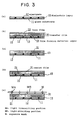
- Fig. 2(a) is a schematic sectional view of the rolled transfer film of the present invention and Fig. 2(b) is a sectional view showing the layer structure of the transfer film [detail view of a portion (X)].
- the transfer film shown in Fig. 2 is a composite film used to form a dielectric layer constituting a PDP as an example of the transfer film of the present invention.
- the transfer film generally comprises a base film F1, a film forming material layer F2 which is formed on the surface of the base film F1 and can be peeled off, and a cover film F3 which is formed on the surface of the film forming material layer F2 and can be peeled off.
- the cover film F3 may not be used according to the properties of the film forming material layer F2.
- the base film F1 constituting the transfer film is preferably a resin film having heat resistance, solvent resistance and flexibility.
- the pasty composition of the present invention can be coated by a roll coater or blade coater, thereby making it possible to form a film forming material layer having uniform thickness and to keep and supply the formed film forming material layer in the form of a roll.
- a resin forming the base film F1 is, for example, polyethylene terephthalate, polyester, polyethylene, polypropylene, polystyrene, polyimide, polyvinyl alcohol, polyvinyl chloride, fluororesin such as polyfluoroethylene, nylon or cellulose.
- the base film F1 has a thickness of 20 to 100 ⁇ m, for example.
- the film forming material layer F2 constituting the transfer film is a layer which turns into a glass sintered body (dielectric layer) by baking and contains glass powders (inorganic particles), a binder resin and a specific plasticizer as essential ingredients.
- the thickness of the film forming material layer F2 which differs according to the content of the glass powders and the type and size of a panel, is 5 to 200 ⁇ m, preferably 10 to 100 ⁇ m.
- the thickness is smaller than 5 ⁇ m, the thickness of the finally formed dielectric layer becomes too small and desired dielectric characteristics may not be ensured.
- this thickness is in the range of 10 to 100 ⁇ m, the thickness of the dielectric layer required for a large-sized panel can be ensured.
- the cover film F3 constituting the transfer film is a film for protecting the surface of the film forming material layer F2 (contact surface with the glass substrate).
- This cover film F3 is preferably a resin film having flexibility.
- Illustrative examples of the resin forming the cover film F3 are the same as those listed for the base film F1.
- the thickness of the cover film F3 is 20 to 100 ⁇ m, for example.
- the transfer film of the present invention can be produced by forming the film forming material layer F2 on the base film F1 and forming the cover film F3 on the film forming material layer F3 (press bonding).
- the composition of the present invention containing inorganic particles, a binder resin, a specific plasticizer and a solvent is coated on the surface of a base film and the coating film is dried to remove part or all of the solvent.
- a roll coater, blade coater such as a doctor blade, curtain coater, wire coater or the like is preferably used because a coating film having excellent thickness uniformity can be efficiently formed.
- the surface of the base film coated with the composition of the present invention is preferably subjected to a release treatment. Thereby, the base film can be easily peeled off from the film forming material layer after the film forming material layer is transferred.
- the coating film of the composition of the present invention formed on the base film is dried to remove part or all of the solvent and turns into a film forming material layer constituting the transfer film.
- Conditions for drying the coating film of the composition of the present invention include a temperature of 40 to 150°C and a time of about 0.1 to 30 minutes.
- the content of the solvent after drying, that is, the content of the solvent in the film forming material layer is preferably 10 wt% or less, more preferably 1 to 5 wt% so as to cause the film forming material layer to exhibit tackiness to the substrate and appropriate shape retention properties.
- the surface of the cover film formed on the film forming material layer formed as described above is preferably subjected to a release treatment as well. Thereby, the cover film can be easily peeled off from the film forming material layer before the film forming material layer is transferred.
- the film forming material layer formed on the base film is transferred to the surface of the substrate en bloc. Since the transfer film of the present invention enables the film forming material layer to be formed on the glass substrate by the above simple operation without fail, the efficiency of the step of forming a constituent element of a PDP such as a dielectric layer can be improved and the improvement of the quality of the formed constituent element, for example, the development of stable dielectric characteristics in the dielectric layer can be realized.
- the production process of the present invention comprises the steps of transferring a film forming material layer constituting the transfer film of the present invention to the surface of a substrate and baking the transferred film forming material layer to form a dielectric layer on the surface of the substrate.
- the film forming material layer F2 formed on the base film F1 is transferred to the surface of the substrate by the above operation.
- Transfer conditions include a heating roll surface temperature of 60 to 120°C, a heating roll pressure of 1 to 5 kg/cm 2 , and a heating roll moving speed of 0.2 to 10.0 m/min.
- This operation can be carried out with a laminator.
- the substrate may be preheated at a temperature of 40 to 100°C, for example.
- the film forming material layer F2 transferred to the surface of the substrate turns into an inorganic sintered body (dielectric layer) by baking.
- Baking is carried out by placing the substrate having the film forming material layer F2 transferred thereto in a high-temperature atmosphere.
- the organic substances for example, the binder resin, residual solvent, specific plasticizer, various additives contained in the film forming material layer F2 are decomposed and removed, and the inorganic particles are molten and sintered.
- the sintering temperature which differs according to the melting temperature of the substrate and the constituent components of the film forming material layer is, for example, 300 to 800°C, preferably 400 to 600°C.
- the production process of the present invention comprises the steps of transferring a film forming material layer constituting the transfer film of the present invention to the surface of a substrate, forming a resist film on the transferred film forming material layer, exposing the resist film to form a resist pattern latent image, developing the resist film to form a resist pattern, etching the film forming material layer to form a pattern layer corresponding to the resist pattern and baking the pattern layer to form a constituent element selected from the group consisting of a barrier, electrode, resistor, dielectric layer, phosphor, color filter and black matrix.
- the production process of the present invention comprises the steps of forming a laminate film consisting of a resist film and a film forming material layer formed of the composition of the present invention on a base film in the order named, transferring the laminate film formed on the base film to the surface of a substrate, exposing the resist film constituting the laminate film to form a resist pattern latent image, developing the resist film to form a resist pattern, etching the film forming material layer to form a pattern layer corresponding to the resist pattern and baking the pattern layer to form a constituent element selected from the group consisting of a barrier, electrode, resistor, dielectric layer, phosphor, color filter and black matrix.
- a method of forming "barriers" which are a constituent element of a PDP on the rear surface of a substrate comprises (1) the step of transferring a film forming material layer, (2) the step of forming a resist film, (3) the step of exposing the resist film, (4) the step of developing the resist film, (5) the step of etching the film forming material layer and (6) the step of baking a barrier pattern to form barriers on the surface of the substrate.
- Figs. 3 and Figs. 4 are schematic sectional views showing a series of steps of forming the barriers.
- reference numeral 11 denotes a glass substrate on which electrodes 12 for generating plasma are arranged at equal intervals and covered with a dielectric layer 13 formed on the surface.
- the expression "transferring a film forming material layer to the surface of a substrate” means not only “transferring the film forming material layer to the surface of the above glass substrate 11" but also “transferrlng the film forming material layer to the surface of the above dielectric layer 13".
- the transfer film 20 is placed upon the surface of the dielectric layer 13 in such a manner that the surface of the film forming material layer 21 comes into contact with the dielectric layer 13 and press-bonded with a heating roll, and the base film 22 is peeled off and removed from the film forming material layer 21.
- the film forming material layer 21 is transferred and closely bonded to the surface of the dielectric layer 13.
- Transfer conditions include a heating roll surface temperature of 80 to 140°C, a heating roll pressure of 1 to 5 kg/cm 2 and a heating roll moving speed of 0.1 to 10.0 m/min.
- the glass substrate 11 may be preheated at a temperature of 40 to 100°C, for example.
- the resist film 31 is formed on the surface of the transferred film forming material layer 21.
- a resist constituting this resist film 31 may be either a positive resist or a negative resist.
- the resist film 31 can be formed by coating a resist by a screen printing method, roll coating method, rotation coating method, cast coating method or the like and drying the coating film.
- the drying temperature of the coating film is generally about 60 to 130°C.
- a resist film formed on the base film may be transferred to the surface of the film forming material layer 21.
- This method can reduce the number of steps of forming the resist film and makes it possible to obtain a resist film having excellent thickness uniformity, whereby the development of the resist film and the etching of the film forming material layer are carried out uniformly and the formed barriers become uniform in height and shape.
- the resist film 31 has a thickness of 0.1 to 40 ⁇ m, preferably 0.5 to 20 ⁇ m.
- the surface of the resist film 31 formed on the film forming material layer 21 is selectively irradiated with (exposed to) radiation such as ultraviolet radiation through an exposure mask M to form a resist pattern latent image.
- radiation such as ultraviolet radiation
- MA and MB signify a light transmitting portion and a light shielding portion formed by the exposure mask M, respectively.
- An irradiation device is not particularly limited and may be an ultraviolet irradiation device used for photolithography and an exposure device used for the production of semiconductors and liquid crystal display devices.
- the exposed resist film is developed to form a resist pattern (latent image).
- the type, composition and concentration of a developer, developing time, developing temperature, developing method (such as an immersion, rocking, shower, spray or puddling method) and developing device may be suitably selected according to the type of the resist film 31.
- a resist pattern 35 (pattern corresponding to the exposure mask M) consisting of resist remaining portions 35A and resist removed portions 35B is formed by this developing step as shown in Fig. 4(f).
- This resist pattern 35 serves as an etching mask in the following step (etching step) and the constituent material (photo-cured resist) of the resist remaining portions 35A must have a lower dissolution speed in an etching solution than the constituent material of the film forming material layer 21.
- step of etching film forming material layer
- the film forming material layer is etched to form a barrier pattern layer corresponding to the resist pattern.
- Fig. 4(g) portions corresponding to the resist removed portions 35B of the resist pattern 35 of the film forming material layer 21 are dissolved in the etching solution and selectively removed.
- Fig. 4(g) shows that the film forming material layer 21 is being etched.
- a barrier pattern layer 25 consisting of material layer remaining portions 25A and material layer removed portions 25B is formed.
- the type, composition and concentration of the etching solution, etching time, etching temperature, etching method (such as an immersion, rocking, shower, spray or puddling method) and etching device may be suitably selected according to the type of the film forming material layer 21.
- the type of the resist film 31 and the type of the film forming material layer 21 are selected such that the same solution as the developer used in the developing step can be used as the etching solution in order to carry out the developing step and the etching step continuously, thereby making it possible to improve production efficiency due to the simplification of the process.
- the resist remaining portions 35A constituting the resist pattern 35 are gradually dissolved by etching and completely removed when the barrier pattern layer 25 is formed (at the end of etching). Even when part or all of the resist remaining portions 35A remain after etching, the resist remaining portions 35A are removed in the following baking step.
- barriers are formed by baking the barrier pattern layer 25.
- the organic substances contained in the material layer remaining portions 25A are calcined and barriers are formed, whereby a panel material 50 having barriers 40 formed on the surface of the dielectric layer 13 as shown in Fig. 4(i) is obtained.
- spaces partitioned by the barriers 40 spaces derived from the material layer removed portions 25B serve as plasma working spaces.
- the baking temperature must be a temperature at which the organic substances contained in the material layer remaining portions (25A) are calcined, generally 400 to 600°C.
- the baking time is generally 10 to 90 minutes.
- the process for forming a PDP in the present invention is not limited to the process shown in Figs. 3 and Figs. 4.
- Electrodes, resistor, dielectric layer, phosphor, color filter and black matrix constituting a PDP can be formed in accordance with this method.
- composition of the present invention having a viscosity of 4,000 cp was prepared by kneading together 100 parts of a PbO-B 2 O 3 -SiO 2 mixture (softening point of 500°C) consisting of 70 wt% of lead oxide, 10 wt% of boron oxide and 20 wt% of silicon oxide, 20 parts of polybutyl methacrylate as a binder resin (weight average molecular weight of 50,000) as a binder resin, 1 part of a compound represented by the following formula (a) (propylene glycol monooleate) as a specific plasticizer and 20 part of propylene glycol monomethyl ether as a solvent with a dispersion mixer.
- a PbO-B 2 O 3 -SiO 2 mixture softening point of 500°C
- a binder resin weight average molecular weight of 50,000
- composition of the present invention prepared in (1) above was coated on a polyethylene terephthalate (PET) base film which had been subjected to a release treatment (width of 400 mm, length of 30 m, thickness of 38 ⁇ m) using a blade coater and the formed coating film was dried at 100°C for 5 minutes to remove the solvent, thereby forming a 50 ⁇ m-thick film forming material layer on the base film.
- PET cover film width of 400 mm, length of 30 m, thickness of 25 ⁇ m
- the obtained transfer film had suppleness and could be easily rolled.
- the film forming material layer had excellent flexibility that the surface of the film forming material layer was not cracked even when this transfer film was bent.
- the cover film was removed from this transfer film and the transfer film (laminate consisting of the base film and the film forming material layer) was placed upon a glass substrate without applying pressure in such a manner that the surface of the film forming material layer came into contact with the surface of the glass substrate, and then the transfer film was removed from the surface of the glass substrate.
- the film forming material layer showed appropriate tackiness to the glass substrate and the transfer film could be removed without causing a cohesive failure in the film forming material layer. Therefore, the transfer film had excellent handling properties.
- the transfer film (laminate consisting of the base film and the film forming material layer) was placed upon a glass substrate for a 20-inch panel in such a manner that the surface of the film forming material layer came into contact with the surface (bus electrode fixed surface) of the glass substrate and press-bonded with a heating roll under heating.
- Press bonding conditions included a heating roll surface temperature of 110°C, a roll pressure of 3 kg/cm and a heating roll moving speed of 1 m/min.
- the base film was peeled off and removed from the film forming material layer fixed (bonded under heating) to the surface of the glass substrate to complete the transfer of the film forming material layer.
- the film forming material layer had sufficiently large film strength that a cohesive failure did not occur in the film forming material layer. Further, the transferred film forming material layer had excellent adhesion to the surface of the glass substrate.
- the glass substrate having the film forming material layer transferred in (3) above was placed in a kiln and baked at 590°C for 30 minutes by elevating the temperature inside the kiln from normal temperature to 590°C at a rate of 10°C/min to form an achromatic transparent dielectric layer made of a glass sintered body on the surface of the glass substrate.
- the thickness (average thickness and tolerance) of this dielectric layer was measured, it was in the range of 30 ⁇ m ⁇ 0.4 ⁇ m.
- the dielectric layer had excellent thickness uniformity.
- composition of the present invention having a viscosity of 4,000 cp was prepared in the same manner as in (1) of Example 1 except that the amount of the compound (specific plasticizer) represented by the above formula (a) was changed to 5 parts and the transfer film of the present invention having suppleness was produced in the same manner as in (2) of Example 1 except that the composition was used.
- the obtained transfer film was used for the evaluation of flexibility and handling properties of the film forming material layer in the same manner as in (2) of Example 1.
- the film forming material layer had excellent flexibility that the surface of the film forming material layer was not cracked (flex cracking) when the transfer film was bent.
- the transfer film had excellent handling properties.
- the film forming material layer was transferred in the same manner as in (3) of Example 1 except that the obtained transfer film was used.
- the film forming material layer had sufficiently large film strength that a cohesive failure did not occur in the film forming material layer when the base film was removed in this transfer step. Further, the transferred film forming material layer had excellent adhesion to the surface of the glass substrate.
- the glass substrate having the film forming material layer transferred thereto was baked in the same manner as in (4) of Example 1 to form an achromatic transparent dielectric layer made of a glass sintered body on the surface of the glass substrate.
- the thickness of the dielectric layer (average film thickness and tolerance) was measured, it was in the range of 30 ⁇ m ⁇ 0.5 ⁇ m. Thus, the dielectric layer had excellent thickness uniformity.
- composition of the present invention having a viscosity of 3,500 cp was prepared in the same manner as in (1) of Example 1 except that 5 parts of a compound represented by the following formula (b) (di-2-ethylhexyl azelate) was used in place of the compound represented by the above formula (a) and the transfer film of the present invention having suppleness was produced in the sane manner as in (2) of Example 1 except that the composition was used.
- the obtained transfer film was used for the evaluation of flexibility and handling properties of the film forming material layer in the same manner as in (2) of Example 1.
- the film forming material layer had excellent flexibility that the surface of the film forming material layer was not cracked (flex cracking) when the transfer film was bent.
- the transfer film had excellent handling properties.
- the film forming material layer was transferred in the same manner as in (3) of Example 1 except that the obtained transfer film was used.
- the film forming material layer had sufficiently large film strength that a cohesive failure did not occur in the film forming material layer when the base film was removed in this transfer step. Further, the transferred film forming material layer had excellent adhesion to the surface of the glass substrate.
- the glass substrate having the film forming material layer transferred thereto was baked in the same manner as in (4) of Example 1 to form an achromatic transparent dielectric layer made of a glass sintered body on the surface of the glass substrate.
- the thickness of the dielectric layer (average film thickness and tolerance) was measured, it was in the range of 30 ⁇ m ⁇ 0.5 ⁇ m. Thus, the dielectric layer had excellent thickness uniformity.
- a composition for comparison having a viscosity of 3,000 cp was prepared in the same manner as in (1) of Example 1 except that a specific plasticizer was not used and a transfer film for comparison was produced in the same manner as in (2) of Example 1 except that the composition was used.
- the obtained transfer film was inferior in suppleness and difficult to be rolled.
- the surface of the film forming material layer was markedly cracked (flex cracking).
- the film forming material layer was inferior in flexibility.
- the film forming material layer was transferred in the same manner as in (3) of Example 1 except that the obtained transfer film was used and further the glass substrate having the film forming material layer transferred thereto was baked in the same manner as in (4) of Example 1 to form an achromatic dielectric layer made of a glass sintered body on the surface of the glass substrate.
- the thickness of the dielectric layer (average film thickness and tolerance) was measured, it was in the range of 30 ⁇ m ⁇ 0.5 ⁇ m.
- a composition having a viscosity of 4,000 cp was prepared in the same manner as in (1) of Example 1 except that the amount of the compound (specific plasticizer) represented by the above formula (a) was changed to 0.1 part and a transfer film was produced in the same manner as in (2) of Example 1 except that the composition was used.
- the obtained transfer film was slightly inferior in suppleness and slightly difficult to be rolled.
- the surface of the film forming material layer was slightly cracked (flex cracking).
- the film forming material layer was transferred in the same manner as in (3) of Example 1 except that the obtained transfer film was used and further the glass substrate having the film forming material layer transferred thereto was baked in the same manner as in (4) of Example 1 to form an achromatic dielectric layer made of a glass sintered body on the surface of the glass substrate.
- the thickness of the dielectric layer (average film thickness and tolerance) was measured, it was in the range of 30 ⁇ m ⁇ 0.5 ⁇ m.
- a composition having a viscosity of 4.500 cp was prepared in the same manner as in (1) of Example 1 except that the amount of the compound (specific plasticizer) represented by the above formula (a) was changed to 20 parts and a transfer film was produced in the same manner as in (2) of Example 1 except that the composition was used.
- the obtained transfer film was used for the evaluation of flexibility of the film forming material layer in the same manner as in (2) of Example 1.
- the film forming material layer had excellent flexibility that the surface of the film forming material layer was not cracked (flex cracking) even when the transfer film was bent.
- the cover film was removed from the transfer film, the transfer film (laminate consisting of the base film and the film forming material layer) was placed upon a glass substrate without applying pressure to the transfer film in such a manner that the surface of the film forming material layer came into contact with the surface of the glass substrate, and then the transfer film was removed from the surface of the glass substrate.
- the tackiness of the film forming material layer to the glass substrate was too large and hence, part of the film forming material layer was adhered to the glass substrate.
- the transfer film was inferior in handling properties.
- the film forming material layer was transferred in the same manner as in (3) of Example 1 except that the obtained transfer film was used and further the glass substrate having the film forming material layer transferred thereto was baked in the sane manner as in (4) of Example 1 to form an achromatic dielectric layer made of a glass sintered body on the surface of the glass substrate.
- the thickness of the dielectric layer (average film thickness and tolerance) was measured, it was in the range of 30 ⁇ m ⁇ 0.5 ⁇ m.
- composition of the present invention for forming electrodes was prepared by kneading together 100 parts of silver powders as inorganic particles, 40 parts of an n-butyl methacrylate/methacrylic acid (weight ratio of 70/30) copolymer (weight average molecular weight of 70,000) as a binder resin, 5 parts of a compound represented by the above formula (a) (propylene glycol monooleate) as a specific plasticizer and 20 part of propylene glycol monomethyl ether as a solvent with a dispersion mixer.
- a pasty alkali development radiation sensitive resist composition was prepared by kneading together 50 parts of an n-butyl methacrylate/methacrylic acid (weight ratio of 85/15) copolymer (weight average molecular weight of 50,000) as an alkali-soluble resin. 40 parts of pentaerythritol tetraacrylate as a polyfunctional monomer (radiation sensitive component), 5 parts of 2-benzyl-2-dimethylamino-1-(4-morpholinophenyl)-butan-1-one as a photopolymerization initiator (radiation sensitive component) and 150 parts of ethyl 3-ethoxypropionic acid as a solvent.
- the resist composition obtained in (2) above was coated on the surface of the same base film as used in Example 1 with a blade coater and the formed coating film was dried at 100°C for 5 minutes to remove the solvent, thereby producing a 5 ⁇ m-thick resist film on the base film. Thereafter, the composition for forming electrodes obtained in (1) above was coated on the surface of the resist film and dried to form a 20 ⁇ m-thick film forming material layer. A cover film was then formed on the film forming material layer in the same manner as in Example 1 to produce the transfer film of the present invention.
- the obtained transfer film was used for the evaluation of flexibility and handling properties of the film forming material layer in the same manner as in (2) of Example 1.
- the film forming material layer had excellent flexibility that the surface of the film forming material layer was not cracked (flex cracking) even when the transfer film was bent.
- This transfer film had excellent handling properties.
- the transfer film was placed upon a glass substrate for a 6-inch panel in such a manner that the surface of the film forming material layer came into contact with the surface of the glass substrate and then press-bonded by a heating roll under heating.
- Press-bonding conditions included a heating roll surface temperature of 120°C, a roll pressure of 4 kg/cm 2 and a heating roll moving speed of 0.5 m/min.
- the base film was peeled off and removed from the resist film to complete the transfer of the laminate film consisting of the film forming material layer and the resist film.
- the film forming material layer had sufficiently large film strength that a cohesive failure did not occur in the film forming material layer. Further, the transferred film forming material layer had excellent adhesion to the surface of the glass substrate.
- the resist film was exposed to an i-ray (ultraviolet light having a wavelength of 365 nm) from an ultra-high pressure mercury lamp through an exposure mask (50 ⁇ m-wide stripe pattern).
- the amount of exposure was 400 mJ/cm 2 .
- the exposed resist film was developed by a shower method using a 0.2 wt% potassium hydroxide aqueous solution (25°C) as a developer for 20 seconds. Thereafter, the resist film was washed with ultra-pure water to remove uncured resist portions not exposed to ultraviolet radiation so as to form a resist pattern.
- the film forming material layer was etched by a shower method using a 0.2 wt% potassium hydroxide aqueous solution (25°C) as an etching solution for 2 minutes. Thereafter, the film forming material layer was washed with ultra-pure water and dried. Thereby, a film forming material layer pattern consisting of material layer remaining portions and material layer removed portions was formed.
- the glass substrate having the film forming material layer pattern formed thereon was baked in a kiln at 600°C for 30 minutes. Thereby, electrodes were formed on the surface of the glass substrate.
- the width at the bottom was 50 ⁇ m ⁇ 2 ⁇ m and the height was 10 ⁇ m ⁇ 1 ⁇ m.
- the dimensional accuracy was very high.
- the transfer film of the present invention provides the following effects:
- the production process of the present invention provides the following effects:
- An inorganic particle-containing composition comprising:
Landscapes
- Chemical & Material Sciences (AREA)
- Organic Chemistry (AREA)
- Chemical Kinetics & Catalysis (AREA)
- Polymers & Plastics (AREA)
- Medicinal Chemistry (AREA)
- Health & Medical Sciences (AREA)
- General Chemical & Material Sciences (AREA)
- Materials Engineering (AREA)
- Geochemistry & Mineralogy (AREA)
- Life Sciences & Earth Sciences (AREA)
- Engineering & Computer Science (AREA)
- Gas-Filled Discharge Tubes (AREA)
- Compositions Of Macromolecular Compounds (AREA)
- Surface Treatment Of Glass (AREA)
- Paints Or Removers (AREA)
- Decoration By Transfer Pictures (AREA)
- Treatments Of Macromolecular Shaped Articles (AREA)
Applications Claiming Priority (2)
| Application Number | Priority Date | Filing Date | Title |
|---|---|---|---|
| JP28029498 | 1998-10-01 | ||
| JP10280294A JP2000109341A (ja) | 1998-10-01 | 1998-10-01 | 無機粒子含有組成物、転写フィルムおよびプラズマディスプレイパネルの製造方法 |
Publications (3)
| Publication Number | Publication Date |
|---|---|
| EP1003199A2 true EP1003199A2 (fr) | 2000-05-24 |
| EP1003199A3 EP1003199A3 (fr) | 2001-12-12 |
| EP1003199B1 EP1003199B1 (fr) | 2004-05-12 |
Family
ID=17622993
Family Applications (1)
| Application Number | Title | Priority Date | Filing Date |
|---|---|---|---|
| EP99119469A Expired - Lifetime EP1003199B1 (fr) | 1998-10-01 | 1999-09-30 | Composition comprenant des particules inorganiques, film de transfer la comprenant et procédé de production pour les écrans au plasma |
Country Status (6)
| Country | Link |
|---|---|
| US (3) | US6339118B1 (fr) |
| EP (1) | EP1003199B1 (fr) |
| JP (1) | JP2000109341A (fr) |
| KR (1) | KR100444915B1 (fr) |
| DE (1) | DE69917186T2 (fr) |
| TW (1) | TW429266B (fr) |
Cited By (6)
| Publication number | Priority date | Publication date | Assignee | Title |
|---|---|---|---|---|
| EP1566368A3 (fr) * | 2004-02-20 | 2006-06-14 | JSR Corporation | Composition de poudre de verre contenant de la résine, film de transfert et procédé pour fabriquer un écran plasma comprenant ce film |
| EP1780181A1 (fr) * | 2005-10-25 | 2007-05-02 | LG Electronics Inc. | Composition de pâte, et une feuille céramique verte, pour former une couche diélectrique, et procédé pour former une couche diélectrique d'un panneau d'affichage à plasma |
| EP1886802A3 (fr) * | 2001-08-03 | 2008-07-30 | NanoGram Corporation | Structure incorporant des mélanges de particules inorganiques-polymères |
| EP1798747A3 (fr) * | 2005-12-14 | 2008-08-20 | LG Electronics Inc. | Procédé de fabrication d'une couche diélectrique d'un panneau d'affichage à plasma |
| EP1783797A3 (fr) * | 2005-11-07 | 2009-07-08 | LG Electronics Inc. | Plaque inférieure pour un écran à plasma et procédé de réalisation d'une telle plaque |
| US7816439B2 (en) | 2001-08-03 | 2010-10-19 | Nanogram Corporation | Structures incorporating polymer-inorganic particle blends |
Families Citing this family (18)
| Publication number | Priority date | Publication date | Assignee | Title |
|---|---|---|---|---|
| JP2001322867A (ja) * | 2000-05-09 | 2001-11-20 | Matsushita Electric Ind Co Ltd | 透光性焼結体と、これを用いた発光管及び放電灯 |
| CN1152778C (zh) | 2000-05-19 | 2004-06-09 | Tdk株式会社 | 具有功能性层的功能性薄膜及带有该功能性层的物体 |
| JP2002170485A (ja) * | 2000-11-30 | 2002-06-14 | Jsr Corp | プラズマディスプレイパネル用転写フィルムおよびプラズマディスプレイパネル |
| JP2003096305A (ja) * | 2001-09-19 | 2003-04-03 | Jsr Corp | 無機粒子含有組成物、転写フィルムおよびプラズマディスプレイパネルの製造方法 |
| KR100455121B1 (ko) * | 2002-02-20 | 2004-11-06 | 엘지전자 주식회사 | 플라즈마 디스플레이 패널의 상판 유전체 제조방법 |
| TWI273624B (en) * | 2003-02-28 | 2007-02-11 | Jsr Corp | Inorganic particle-containing composition, transfer film comprising the same and plasma display panel production process |
| US20060043634A1 (en) * | 2004-08-26 | 2006-03-02 | 3M Innovative Properties Company | Method of forming microstructures with a discrete mold provided on a roller |
| US7670543B2 (en) * | 2004-08-26 | 2010-03-02 | 3M Innovative Properties Company | Method of forming microstructures with a template |
| US20060043638A1 (en) * | 2004-08-26 | 2006-03-02 | 3M Innovative Properties Company | Method of forming microstructures with multiple discrete molds |
| KR100738234B1 (ko) * | 2004-12-14 | 2007-07-12 | 엘지전자 주식회사 | 플라즈마 디스플레이 패널 제조용 그린 쉬트 및 플라즈마 디스플레이 패널 |
| JP4572687B2 (ja) * | 2005-01-14 | 2010-11-04 | ソニー株式会社 | バックライト装置及び液晶表示装置 |
| KR20070043151A (ko) * | 2005-10-20 | 2007-04-25 | 삼성전기주식회사 | 실란 헤드를 갖는 분산제 및 그를 포함하는 형광체페이스트 조성물 |
| JP2007137939A (ja) * | 2005-11-15 | 2007-06-07 | Jsr Corp | 無機粉体含有樹脂組成物、転写フィルム、パネル部材の形成方法およびプラズマディスプレイパネルの製造方法 |
| JP4849612B2 (ja) * | 2006-10-19 | 2012-01-11 | 日東電工株式会社 | 無機粉体含有樹脂組成物及び誘電体層形成基板 |
| KR101206250B1 (ko) | 2009-10-13 | 2012-11-28 | 주식회사 엘지화학 | 식각 마스크 패턴 형성용 페이스트 및 이의 스크린 인쇄법을 이용한 실리콘 태양전지의 제조방법 |
| US20110094579A1 (en) * | 2009-10-26 | 2011-04-28 | Yukika Yamada | Electrode substrate, method of preparing same, and photoelectric conversion device including same |
| CA2937376A1 (fr) | 2014-02-26 | 2015-09-03 | Elevance Renewable Sciences, Inc. | Compositions a faible teneur en cov, leurs procedes de fabrication et utilisation |
| US11120821B2 (en) * | 2016-08-08 | 2021-09-14 | Plantronics, Inc. | Vowel sensing voice activity detector |
Family Cites Families (24)
| Publication number | Priority date | Publication date | Assignee | Title |
|---|---|---|---|---|
| CS173141B1 (fr) * | 1973-07-16 | 1977-02-28 | ||
| US4129489A (en) * | 1976-02-14 | 1978-12-12 | Ppg Industries, Inc. | Preparation of polymer based powder coatings by ionizing radiation |
| CA1175989A (fr) * | 1981-09-23 | 1984-10-09 | Polysar Limited | Methode de preparation de compositions durcissables |
| US5188693A (en) * | 1986-04-18 | 1993-02-23 | Aishin Kakou K.K. | Process for applying polyvinyl chloride sealing material having low thixotropic index |
| US5133974A (en) * | 1989-05-05 | 1992-07-28 | Kv Pharmaceutical Company | Extended release pharmaceutical formulations |
| JP3229640B2 (ja) | 1992-01-28 | 2001-11-19 | 大日本印刷株式会社 | プラズマディスプレイパネルの蛍光面形成方法及びそれに使用するプラズマディスプレイパネル用蛍光体スラリー |
| JP3229639B2 (ja) | 1992-01-28 | 2001-11-19 | 大日本印刷株式会社 | プラズマディスプレイパネルの蛍光面形成方法及びそれに使用するプラズマディスプレイパネル用蛍光体スラリー |
| JP3229641B2 (ja) | 1992-01-28 | 2001-11-19 | 大日本印刷株式会社 | プラズマディスプレイパネルの蛍光面形成方法及びそれに使用するプラズマディスプレイパネル用蛍光体スラリー |
| JPH0675372A (ja) | 1992-08-28 | 1994-03-18 | Toppan Printing Co Ltd | 感光性着色組成物およびカラーフィルターの製造方法およびカラーフィルター |
| JP3343397B2 (ja) | 1993-05-11 | 2002-11-11 | 旭硝子株式会社 | 誘電体ペースト |
| JP2705530B2 (ja) | 1993-09-06 | 1998-01-28 | 日本電気株式会社 | プラズマディスプレイパネル及びその製造方法 |
| AUPM807094A0 (en) * | 1994-09-09 | 1994-10-06 | Commonwealth Scientific And Industrial Research Organisation | Polymer beads and method for preparation thereof |
| JPH08139230A (ja) * | 1994-11-11 | 1996-05-31 | Sumitomo Kinzoku Ceramics:Kk | セラミック回路基板とその製造方法 |
| JPH09102273A (ja) | 1995-08-01 | 1997-04-15 | Japan Synthetic Rubber Co Ltd | プラズマディスプレイパネルの製造方法 |
| JP3758220B2 (ja) | 1995-11-17 | 2006-03-22 | 東レ株式会社 | 感光性導電ペーストおよび電極の製造方法 |
| JPH09208611A (ja) | 1996-02-06 | 1997-08-12 | Japan Synthetic Rubber Co Ltd | 螢光体分散感放射線性組成物 |
| US5929133A (en) * | 1996-02-16 | 1999-07-27 | Hitachi Chemical Filtec, Inc. | Anti-bacterial film suitable for food packaging |
| US5980347A (en) | 1996-07-25 | 1999-11-09 | Jsr Corporation | Process for manufacturing plasma display panel |
| JPH10233156A (ja) * | 1997-02-17 | 1998-09-02 | Dainippon Printing Co Ltd | プラズマディスプレイパネル作製方法 |
| JPH10291834A (ja) | 1997-04-18 | 1998-11-04 | Jsr Corp | 誘電体層形成用転写フィルムおよび誘電体層形成用組成物 |
| US5866312A (en) * | 1997-06-19 | 1999-02-02 | Eastman Kodak Company | Photographic element having surface protective layer |
| TWI231293B (en) * | 1997-11-12 | 2005-04-21 | Jsr Corp | Transfer film |
| JP3570475B2 (ja) | 1997-11-26 | 2004-09-29 | Jsr株式会社 | 転写フィルムおよびそれを用いたプラズマディスプレイパネルの製造方法 |
| JP2000053444A (ja) * | 1998-08-07 | 2000-02-22 | Jsr Corp | ガラスペースト組成物、転写フィルムおよびプラズマディスプレイパネル |
-
1998
- 1998-10-01 JP JP10280294A patent/JP2000109341A/ja active Pending
-
1999
- 1999-09-30 US US09/409,074 patent/US6339118B1/en not_active Expired - Lifetime
- 1999-09-30 EP EP99119469A patent/EP1003199B1/fr not_active Expired - Lifetime
- 1999-09-30 DE DE69917186T patent/DE69917186T2/de not_active Expired - Lifetime
- 1999-10-01 KR KR10-1999-0042177A patent/KR100444915B1/ko not_active Expired - Fee Related
- 1999-10-01 TW TW088116968A patent/TW429266B/zh not_active IP Right Cessation
-
2001
- 2001-09-27 US US09/963,488 patent/US6548582B2/en not_active Expired - Lifetime
- 2001-11-19 US US09/988,305 patent/US6956076B2/en not_active Expired - Lifetime
Cited By (9)
| Publication number | Priority date | Publication date | Assignee | Title |
|---|---|---|---|---|
| EP1886802A3 (fr) * | 2001-08-03 | 2008-07-30 | NanoGram Corporation | Structure incorporant des mélanges de particules inorganiques-polymères |
| US7816439B2 (en) | 2001-08-03 | 2010-10-19 | Nanogram Corporation | Structures incorporating polymer-inorganic particle blends |
| US8648136B2 (en) | 2001-08-03 | 2014-02-11 | Nanogram Corporation | Structures incorporating polymer-inorganic particle blends |
| EP1566368A3 (fr) * | 2004-02-20 | 2006-06-14 | JSR Corporation | Composition de poudre de verre contenant de la résine, film de transfert et procédé pour fabriquer un écran plasma comprenant ce film |
| EP1780181A1 (fr) * | 2005-10-25 | 2007-05-02 | LG Electronics Inc. | Composition de pâte, et une feuille céramique verte, pour former une couche diélectrique, et procédé pour former une couche diélectrique d'un panneau d'affichage à plasma |
| US7651737B2 (en) | 2005-10-25 | 2010-01-26 | Lg Electronics Inc. | Paste composition, and a green sheet, for forming a dielectric layer, and a method for forming a dielectric layer of plasma display panel |
| EP1783797A3 (fr) * | 2005-11-07 | 2009-07-08 | LG Electronics Inc. | Plaque inférieure pour un écran à plasma et procédé de réalisation d'une telle plaque |
| US7758395B2 (en) | 2005-11-07 | 2010-07-20 | Lg Electronics Inc. | Lower plate of PDP and method for manufacturing the same |
| EP1798747A3 (fr) * | 2005-12-14 | 2008-08-20 | LG Electronics Inc. | Procédé de fabrication d'une couche diélectrique d'un panneau d'affichage à plasma |
Also Published As
| Publication number | Publication date |
|---|---|
| DE69917186D1 (de) | 2004-06-17 |
| US20020035183A1 (en) | 2002-03-21 |
| KR100444915B1 (ko) | 2004-08-18 |
| US20020016401A1 (en) | 2002-02-07 |
| DE69917186T2 (de) | 2005-05-25 |
| EP1003199A3 (fr) | 2001-12-12 |
| EP1003199B1 (fr) | 2004-05-12 |
| JP2000109341A (ja) | 2000-04-18 |
| US6339118B1 (en) | 2002-01-15 |
| US6956076B2 (en) | 2005-10-18 |
| TW429266B (en) | 2001-04-11 |
| US6548582B2 (en) | 2003-04-15 |
| KR20000028762A (ko) | 2000-05-25 |
Similar Documents
| Publication | Publication Date | Title |
|---|---|---|
| EP1003199B1 (fr) | Composition comprenant des particules inorganiques, film de transfer la comprenant et procédé de production pour les écrans au plasma | |
| JP4075277B2 (ja) | 無機粒子含有感光性組成物および感光性フィルム | |
| KR100852295B1 (ko) | 무기 입자 함유 조성물, 전사 필름 및 플라즈마디스플레이 패널의 제조 방법 | |
| JP4103776B2 (ja) | 無機粒子含有組成物、転写フィルムおよびプラズマディスプレイパネルの製造方法 | |
| CN1733845B (zh) | 含有无机粉末的树脂组合物、转印薄膜及等离子显示器面板的制造方法 | |
| JP4006907B2 (ja) | 感光性転写フィルム | |
| JP2008077069A (ja) | 無機粉体含有樹脂組成物、転写フィルムおよびフラットパネルディスプレイの製造方法 | |
| JP4366820B2 (ja) | 無機粒子含有感光性組成物および感光性フィルム | |
| JP2006219660A (ja) | 無機粉体含有樹脂組成物、転写フィルムおよびプラズマディスプレイパネルの製造方法 | |
| EP1452558A1 (fr) | Composition comprenant des particules inorganiques, film de transfer la comprenant et procédé de production pour les écrans au plasma | |
| KR100869398B1 (ko) | 플라즈마 디스플레이 패널의 제조 방법 및 전사 필름 | |
| KR100859392B1 (ko) | 플라즈마 디스플레이 패널용 무기 입자 함유 조성물, 전사필름 및 플라즈마 디스플레이 패널의 제조 방법 | |
| JP2006233031A (ja) | 無機粒子含有組成物、転写フィルムおよびプラズマディスプレイパネルの製造方法 | |
| JP2007137939A (ja) | 無機粉体含有樹脂組成物、転写フィルム、パネル部材の形成方法およびプラズマディスプレイパネルの製造方法 | |
| JP2003071962A (ja) | 転写フィルム | |
| JP2007056117A (ja) | 無機粒子含有樹脂組成物、転写フィルムおよびプラズマディスプレイパネルの製造方法 | |
| JP2009040619A (ja) | フラットパネルディスプレイ部材形成用組成物 | |
| JP2006228506A (ja) | 無機粉体含有樹脂組成物、転写フィルムおよびプラズマディスプレイパネルの製造方法 | |
| JP2003100205A (ja) | プラズマディスプレイパネルの製造方法および転写フィルム | |
| JP2008074681A (ja) | 無機粉体含有樹脂組成物、転写フィルムおよびフラットパネルディスプレイパネルの製造方法 | |
| JP2005322590A (ja) | ディスプレイデバイス隔壁の形成方法とそれに用いられるディスプレイデバイス隔壁形成用塗料 | |
| JP2009270055A (ja) | フラットパネルディスプレイ部材形成用組成物 | |
| JP2001264967A (ja) | 無機粒子含有感光性組成物および感光性フィルム | |
| JP2008034153A (ja) | 無機粉体含有樹脂組成物、転写フィルムおよびフラットパネルディスプレイの製造方法 | |
| KR20060125580A (ko) | 무기 분체 함유 수지 조성물, 전사 필름 및 플라즈마디스플레이 패널의 제조 방법 |
Legal Events
| Date | Code | Title | Description |
|---|---|---|---|
| PUAI | Public reference made under article 153(3) epc to a published international application that has entered the european phase |
Free format text: ORIGINAL CODE: 0009012 |
|
| AK | Designated contracting states |
Kind code of ref document: A2 Designated state(s): AT BE CH CY DE DK ES FI FR GB GR IE IT LI LU MC NL PT SE Kind code of ref document: A2 Designated state(s): DE FR GB NL |
|
| AX | Request for extension of the european patent |
Free format text: AL;LT;LV;MK;RO;SI |
|
| PUAL | Search report despatched |
Free format text: ORIGINAL CODE: 0009013 |
|
| AK | Designated contracting states |
Kind code of ref document: A3 Designated state(s): AT BE CH CY DE DK ES FI FR GB GR IE IT LI LU MC NL PT SE |
|
| AX | Request for extension of the european patent |
Free format text: AL;LT;LV;MK;RO;SI |
|
| RIC1 | Information provided on ipc code assigned before grant |
Free format text: 7H 01J 29/00 A, 7C 08K 3/08 B, 7C 08K 13/02 B, 7C 08K 5/10 B |
|
| 17P | Request for examination filed |
Effective date: 20020424 |
|
| AKX | Designation fees paid |
Free format text: DE FR GB NL |
|
| 17Q | First examination report despatched |
Effective date: 20021217 |
|
| GRAP | Despatch of communication of intention to grant a patent |
Free format text: ORIGINAL CODE: EPIDOSNIGR1 |
|
| RAP1 | Party data changed (applicant data changed or rights of an application transferred) |
Owner name: JSR CORPORATION |
|
| GRAS | Grant fee paid |
Free format text: ORIGINAL CODE: EPIDOSNIGR3 |
|
| GRAA | (expected) grant |
Free format text: ORIGINAL CODE: 0009210 |
|
| AK | Designated contracting states |
Kind code of ref document: B1 Designated state(s): DE FR GB NL |
|
| REG | Reference to a national code |
Ref country code: GB Ref legal event code: FG4D |
|
| REG | Reference to a national code |
Ref country code: IE Ref legal event code: FG4D |
|
| REF | Corresponds to: |
Ref document number: 69917186 Country of ref document: DE Date of ref document: 20040617 Kind code of ref document: P |
|
| ET | Fr: translation filed | ||
| PLBE | No opposition filed within time limit |
Free format text: ORIGINAL CODE: 0009261 |
|
| STAA | Information on the status of an ep patent application or granted ep patent |
Free format text: STATUS: NO OPPOSITION FILED WITHIN TIME LIMIT |
|
| 26N | No opposition filed |
Effective date: 20050215 |
|
| REG | Reference to a national code |
Ref country code: IE Ref legal event code: MM4A |
|
| REG | Reference to a national code |
Ref country code: FR Ref legal event code: PLFP Year of fee payment: 18 |
|
| REG | Reference to a national code |
Ref country code: FR Ref legal event code: PLFP Year of fee payment: 19 |
|
| REG | Reference to a national code |
Ref country code: FR Ref legal event code: PLFP Year of fee payment: 20 |
|
| PGFP | Annual fee paid to national office [announced via postgrant information from national office to epo] |
Ref country code: DE Payment date: 20180920 Year of fee payment: 20 Ref country code: FR Payment date: 20180924 Year of fee payment: 20 |
|
| PGFP | Annual fee paid to national office [announced via postgrant information from national office to epo] |
Ref country code: GB Payment date: 20180919 Year of fee payment: 20 Ref country code: NL Payment date: 20180919 Year of fee payment: 20 |
|
| REG | Reference to a national code |
Ref country code: DE Ref legal event code: R071 Ref document number: 69917186 Country of ref document: DE |
|
| REG | Reference to a national code |
Ref country code: NL Ref legal event code: MK Effective date: 20190929 |
|
| REG | Reference to a national code |
Ref country code: GB Ref legal event code: PE20 Expiry date: 20190929 |
|
| PG25 | Lapsed in a contracting state [announced via postgrant information from national office to epo] |
Ref country code: GB Free format text: LAPSE BECAUSE OF EXPIRATION OF PROTECTION Effective date: 20190929 |