EP1003213A2 - Verfahren zur Herstellung von harzverkapselten Halbleiteranordnungen - Google Patents
Verfahren zur Herstellung von harzverkapselten Halbleiteranordnungen Download PDFInfo
- Publication number
- EP1003213A2 EP1003213A2 EP99122090A EP99122090A EP1003213A2 EP 1003213 A2 EP1003213 A2 EP 1003213A2 EP 99122090 A EP99122090 A EP 99122090A EP 99122090 A EP99122090 A EP 99122090A EP 1003213 A2 EP1003213 A2 EP 1003213A2
- Authority
- EP
- European Patent Office
- Prior art keywords
- insulating board
- device carrier
- resin layer
- carrier areas
- semiconductor chips
- Prior art date
- Legal status (The legal status is an assumption and is not a legal conclusion. Google has not performed a legal analysis and makes no representation as to the accuracy of the status listed.)
- Granted
Links
Images


Classifications
-
- H—ELECTRICITY
- H10—SEMICONDUCTOR DEVICES; ELECTRIC SOLID-STATE DEVICES NOT OTHERWISE PROVIDED FOR
- H10W—GENERIC PACKAGES, INTERCONNECTIONS, CONNECTORS OR OTHER CONSTRUCTIONAL DETAILS OF DEVICES COVERED BY CLASS H10
- H10W74/00—Encapsulations, e.g. protective coatings
- H10W74/01—Manufacture or treatment
- H10W74/014—Manufacture or treatment using batch processing
-
- H—ELECTRICITY
- H10—SEMICONDUCTOR DEVICES; ELECTRIC SOLID-STATE DEVICES NOT OTHERWISE PROVIDED FOR
- H10W—GENERIC PACKAGES, INTERCONNECTIONS, CONNECTORS OR OTHER CONSTRUCTIONAL DETAILS OF DEVICES COVERED BY CLASS H10
- H10W74/00—Encapsulations, e.g. protective coatings
- H10W74/01—Manufacture or treatment
-
- H—ELECTRICITY
- H10—SEMICONDUCTOR DEVICES; ELECTRIC SOLID-STATE DEVICES NOT OTHERWISE PROVIDED FOR
- H10W—GENERIC PACKAGES, INTERCONNECTIONS, CONNECTORS OR OTHER CONSTRUCTIONAL DETAILS OF DEVICES COVERED BY CLASS H10
- H10W74/00—Encapsulations, e.g. protective coatings
- H10W74/10—Encapsulations, e.g. protective coatings characterised by their shape or disposition
- H10W74/111—Encapsulations, e.g. protective coatings characterised by their shape or disposition the semiconductor body being completely enclosed
- H10W74/114—Encapsulations, e.g. protective coatings characterised by their shape or disposition the semiconductor body being completely enclosed by a substrate and the encapsulations
-
- H—ELECTRICITY
- H10—SEMICONDUCTOR DEVICES; ELECTRIC SOLID-STATE DEVICES NOT OTHERWISE PROVIDED FOR
- H10W—GENERIC PACKAGES, INTERCONNECTIONS, CONNECTORS OR OTHER CONSTRUCTIONAL DETAILS OF DEVICES COVERED BY CLASS H10
- H10W90/00—Package configurations
-
- H—ELECTRICITY
- H10—SEMICONDUCTOR DEVICES; ELECTRIC SOLID-STATE DEVICES NOT OTHERWISE PROVIDED FOR
- H10W—GENERIC PACKAGES, INTERCONNECTIONS, CONNECTORS OR OTHER CONSTRUCTIONAL DETAILS OF DEVICES COVERED BY CLASS H10
- H10W72/00—Interconnections or connectors in packages
- H10W72/01—Manufacture or treatment
- H10W72/0198—Manufacture or treatment batch processes
-
- H—ELECTRICITY
- H10—SEMICONDUCTOR DEVICES; ELECTRIC SOLID-STATE DEVICES NOT OTHERWISE PROVIDED FOR
- H10W—GENERIC PACKAGES, INTERCONNECTIONS, CONNECTORS OR OTHER CONSTRUCTIONAL DETAILS OF DEVICES COVERED BY CLASS H10
- H10W72/00—Interconnections or connectors in packages
- H10W72/071—Connecting or disconnecting
- H10W72/075—Connecting or disconnecting of bond wires
-
- H—ELECTRICITY
- H10—SEMICONDUCTOR DEVICES; ELECTRIC SOLID-STATE DEVICES NOT OTHERWISE PROVIDED FOR
- H10W—GENERIC PACKAGES, INTERCONNECTIONS, CONNECTORS OR OTHER CONSTRUCTIONAL DETAILS OF DEVICES COVERED BY CLASS H10
- H10W72/00—Interconnections or connectors in packages
- H10W72/851—Dispositions of multiple connectors or interconnections
- H10W72/874—On different surfaces
- H10W72/884—Die-attach connectors and bond wires
-
- H—ELECTRICITY
- H10—SEMICONDUCTOR DEVICES; ELECTRIC SOLID-STATE DEVICES NOT OTHERWISE PROVIDED FOR
- H10W—GENERIC PACKAGES, INTERCONNECTIONS, CONNECTORS OR OTHER CONSTRUCTIONAL DETAILS OF DEVICES COVERED BY CLASS H10
- H10W72/00—Interconnections or connectors in packages
- H10W72/90—Bond pads, in general
- H10W72/931—Shapes of bond pads
- H10W72/932—Plan-view shape, i.e. in top view
-
- H—ELECTRICITY
- H10—SEMICONDUCTOR DEVICES; ELECTRIC SOLID-STATE DEVICES NOT OTHERWISE PROVIDED FOR
- H10W—GENERIC PACKAGES, INTERCONNECTIONS, CONNECTORS OR OTHER CONSTRUCTIONAL DETAILS OF DEVICES COVERED BY CLASS H10
- H10W72/00—Interconnections or connectors in packages
- H10W72/90—Bond pads, in general
- H10W72/951—Materials of bond pads
-
- H—ELECTRICITY
- H10—SEMICONDUCTOR DEVICES; ELECTRIC SOLID-STATE DEVICES NOT OTHERWISE PROVIDED FOR
- H10W—GENERIC PACKAGES, INTERCONNECTIONS, CONNECTORS OR OTHER CONSTRUCTIONAL DETAILS OF DEVICES COVERED BY CLASS H10
- H10W74/00—Encapsulations, e.g. protective coatings
-
- H—ELECTRICITY
- H10—SEMICONDUCTOR DEVICES; ELECTRIC SOLID-STATE DEVICES NOT OTHERWISE PROVIDED FOR
- H10W—GENERIC PACKAGES, INTERCONNECTIONS, CONNECTORS OR OTHER CONSTRUCTIONAL DETAILS OF DEVICES COVERED BY CLASS H10
- H10W90/00—Package configurations
- H10W90/701—Package configurations characterised by the relative positions of pads or connectors relative to package parts
- H10W90/731—Package configurations characterised by the relative positions of pads or connectors relative to package parts of die-attach connectors
- H10W90/736—Package configurations characterised by the relative positions of pads or connectors relative to package parts of die-attach connectors between a chip and a stacked lead frame, conducting package substrate or heat sink
-
- H—ELECTRICITY
- H10—SEMICONDUCTOR DEVICES; ELECTRIC SOLID-STATE DEVICES NOT OTHERWISE PROVIDED FOR
- H10W—GENERIC PACKAGES, INTERCONNECTIONS, CONNECTORS OR OTHER CONSTRUCTIONAL DETAILS OF DEVICES COVERED BY CLASS H10
- H10W90/00—Package configurations
- H10W90/701—Package configurations characterised by the relative positions of pads or connectors relative to package parts
- H10W90/751—Package configurations characterised by the relative positions of pads or connectors relative to package parts of bond wires
- H10W90/756—Package configurations characterised by the relative positions of pads or connectors relative to package parts of bond wires between a chip and a stacked lead frame, conducting package substrate or heat sink
Definitions
- the present invention relates to a method of fabricating a semiconductor device, and more particularly to a method of fabricating a semiconductor device having a reduced package contour, a reduced mounting area, and a reduced cost.
- the lead frame comprises a rectangular or hooped frame. A plurality of semiconductor devices are simultaneously sealed in one sealing process.
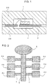
- FIG. 1 of the accompanying drawings illustrates a conventional transfer molding process.
- a lead frame 2 to which semiconductor chips 1 are fixed by die bonding and wire bonding is placed in a cavity 4 defined by upper and lower molds 3A, 3B.
- Epoxy resin is then poured into the cavity 4 to seal the semiconductor chips 1.
- the lead frame 2 is cut off into segments containing the respective semiconductor chips 1, thus producing individual semiconductor devices.
- Japanese laid-open patent publication No. 05-129473 for example.
- the lower mold 3B has a number of cavities 4a - 4f, a source 5 of synthetic resin, a runner 6 connected to the source 5 of synthetic resin, and gates 7 for pouring the synthetic resin from the runner 6 into the cavities 4a - 4f.
- the cavities 4a - 4f, the source 5 of synthetic resin, the runner 6, and the gates 7 are all in the form of recesses and grooves defined in the surface of the lower mold 3B.
- the lead frame 2 is of a rectangular shape, then ten semiconductor chips 1 are mounted on one lead frame, and the lower mold 3B has ten cavities 4, ten gates 7, and one runner 6 per lead frame.
- the entire lower mold 3B has as many as cavities 4 as necessary for twenty lead frames 2, for example.
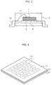
- FIG. 3 of the accompanying drawings shows a semiconductor device fabricated by the conventional transfer molding process.
- a semiconductor chip 1 containing components such as transistors is fixedly mounted on an island 8 of a lead frame by a bonding material 9 such as solder.
- the semiconductor chip 1 has electrode pads connected to leads 10 by wires 11, and has its peripheral portions covered with a molded body 12 of synthetic resin which is complementary in shape to the cavity 4.
- the leads 10 have respective distal ends projecting out of the molded body 12 of synthetic resin.
- the leads 10 for connection to external circuits projects from the molded body 12 of synthetic resin, dimensions of the package that extend up to the projecting distal ends of the leads 10 need to be considered as covering a mounting area of the package. Therefore, the mounting area of the package is much larger than the contour of the molded body 12 of synthetic resin.
- the synthetic resin is also hardened in the runner 6 and the gates 7, and the hardened synthetic resin in the runner 6 and the gates 7 has to be thrown away. Because the gates 7 are required for respective individual semiconductor devices to be fabricated, the synthetic resin is not utilized highly efficiently, but the number of semiconductor devices that can be fabricated is small relatively to the amount of synthetic resin used.
- Another object of the present invention is to provide a method of fabricating a semiconductor device relatively inexpensively.
- a method of fabricating a semiconductor device comprising the steps of preparing an insulating board with a plurality of device carrier areas thereon, fixing semiconductor chips respectively to the device carrier areas, placing an electrode pattern serving as external electrodes of the semiconductor chips on a back of the insulating board, covering the semiconductor chips with a resin layer, and separating the resin layer and the insulating board into segments including the device carrier areas thereby to produce individual semiconductor devices, the electrode pattern being spaced inwardly from edges of the segments.
- a method of fabricating a semiconductor device according to the present invention will be described below in terms of successive steps thereof with reference to FIGS. 4 through 8A - 8C.
- a large-size common board 21 having a two-dimensional matrix of 100 device carrier areas 20 each corresponding to a semiconductor device.
- the common board 21 comprises one or more insulating boards of ceramics, glass epoxy, or the like, and has a total thickness ranging from 250 to 350 ⁇ m to provide a mechanical strength large enough to withstand stresses imposed during the fabrication process.
- the common board 21 comprises a first insulating board 22 having a thickness of about 100 ⁇ m and a second insulating board 23 having a thickness of about 200 ⁇ m, the first and second insulating boards 22, 23 being superposed one on the other.
- An electrically conductive pattern made of printed metal paste of tungsten or the like and electroplated gold is formed on the surface of each of the device carrier areas 20.
- the first and second insulating boards 22, 23 each with printed metal paste of tungsten or the like are bonded to each other and then baked, after which a plated layer of gold is formed on the printed metal paste by an electroplating process.
- FIG. 5A shows in plan an electrically conductive pattern formed on the face of the first insulating board 22
- FIG. 5B shows in plan an electrically conductive pattern formed on the back of the first insulating board 22.
- Each of the device carrier areas 20, enclosed by the dotted lines, has a rectangular shape having a longer side which is 1.0 mm long and a shorter side which is 0.8 mm long.
- the device carrier areas 20 are arranged in a two-dimensional matrix, and adjacent ones of the device carrier areas 20 are spaced from each other by a distance ranging from 20 to 50 ⁇ m. The spacing between adjacent ones of the device carrier areas 20 serves as a dicing line 24 in a subsequent step.
- the electrically conductive pattern provides an island 25 and leads 26.
- the electrically conductive pattern segments in the device carrier areas 20 are identical in shape to each other.
- the island 25 is a region where a semiconductor chip is to be mounted, and the leads 26 are to be connected by wires to electrode pads of a semiconductor chip on the island 25.
- Two first joint arms 27, each having a width of 0.5 mm, for example, much smaller than the width of the island 25, extend continuously from the island 25 across the dicing line 24 to the leads 26 of an adjacent device carrier area 20.
- Two second joint arms 28 extend continuously from the island 25 in directions perpendicular to the first joint arms 27 across the dicing lines 24 to the leads 26 of adjacent device carrier areas 20. Some of the second joint arms 28 are connected to a common joint 29 extending around the device carrier areas 20.
- the first and second joint arms 27, 28 which are thus extended and connected electrically connect the islands 25 and the leads 26 to each other.
- the first insulating board 22 has through holes 30 defined in each of the device carrier areas 20.
- An electrically conductive material such as tungsten is filled in the through holes 30.
- External electrodes 31a, 31b, 31c, 31d are formed on the back of the first insulating board 22 in alignment with the respective through holes 30.
- the external electrodes 31a, 31b, 31c, 31d are spaced or retracted a distance ranging from 0.05 to 0.1 mm inwardly from the edges of each of the device carrier areas 20, and electrically connected to the common joint 29 via the through holes 30.
- FIG. 6A shows in plan the second insulating board 23 bonded to the first insulating board 22, and FIG. 6B shows in cross section the second insulating board 23 bonded to the first insulating board 22.
- the second insulating board 23 has openings 40 extending over the islands 25 and leads 32a, 32b vertically aligned with the leads 26.
- the second insulating board 23 has through holes 33 defined therein in alignment with the leads 32a, 32b and electrically connected to the respective leads 26 on the first insulating board 22. Therefore, the leads 26 are electrically connected to the external electrodes 31c, 31d.
- the leads 32a, 32b are spaced or retracted a distance ranging from about 0.05 to 0.1 mm inwardly from the edges of each of the device carrier areas 20. Only the first and second joint arms 27, 28 of the narrow width extend across the dicing lines 24.
- a plated layer of gold of the electrically conductive pattern is formed by the electroplating process which employs the electrically conductive pattern as one electrode. Since the electrically conductive pattern segments in the device carrier areas 20 are electrically connected to each other by the common joint 29, it is possible to employ the electroplating process. However, no plated layer is formed on the mating surfaces of the first and second insulating boards 22, 23.
- Semiconductor chips 33 are mounted on the respective device carrier areas 20 of the common board 21 with the plated layer of gold, by die bonding and wire bonding. Specifically, the semiconductor chips 33 are fixed to the surfaces of the islands 25 by an adhesive such as an Ag paste, and the electrode pads of the semiconductor chips 33 are connected to the leads 32a, 32b by wires 34.
- the semiconductor chips 33 comprise three-terminal active components such as bipolar transistors, power MOSFETs, or the like. If the semiconductor chips 33 comprise power MOSFETs, then the external electrodes 31a, 31b serve as drain electrodes, and the external electrodes 31c, 31d serve as source and drain electrodes, respectively.
- a predetermined amount of liquid epoxy resin is dropped from a dispenser delivered to a position over the common board 21 by potting to cover all the semiconductor chips 33 with a common resin layer 35.
- the liquid epoxy resin may be CV576AN (manufactured by Matsushita Electric Works, Ltd.). Since the dropped liquid epoxy resin is relatively highly viscous and has a surface tension, the common resin layer 35 has a round surface.
- the round surface of the common resin layer 35 is processed into a flat surface.
- a flat member may be pressed against the round surface of the common resin layer 35 to flatten the surface before the dropped liquid resin is hardened, or after the dropped liquid resin is cured at a temperature ranging from 100 to 200 degrees for several hours, the round surface of the common resin layer 35 may be cut to a flat surface by a dicing device with a dicing blade. Specifically, the round surface of the common resin layer 35 may be scraped off by the dicing blade to achieve a constant height from the common board 21. In this step, the thickness of the common resin layer 35 is set to 0.3 - 1.0 mm.
- the flat surface extends to the edges of the common resin layer 35 such that when outermost semiconductor chips 33 are separated into individual semiconductor devices, they have resin layer contours which meet a standardized package size requirement.
- a relatively thick dicing blade is used to scrape the round surface of the common resin layer 35 repeatedly a plurality of times to develop a flat surface.
- the common resin layer 35 is severed into segments containing the respective device carrier areas 20 to separate individual semiconductor devices by a dicing device.
- a dicing blade 36 is used to cut off the common resin layer 35 and the common board 21 simultaneously along the dicing lines 24 to produce separate semiconductor devices on the respective device carrier areas 20.
- a blue sheet e.g., trade name: UV SHEET manufactured by Lintec Corp.
- the dicing blade 36 is thrust to such a depth as to reach the surface of the blue sheet thereby to cut off the common resin layer 35 and the common board 21.
- the dicing device automatically recognizes alignment marks on the surface of the common board 21 and uses the alignment marks as a positional reference in the dicing process.
- FIGS. 8A through 8C show a semiconductor device 33 fabricated by the above successive steps.
- Each package of the semiconductor device 33 has four sides defined by cut edges of the resin layer 35 and the common board 21, an upper surface defined by the flat surface of the resin layer 35, and a lower surface defined by the back of the first insulating board 22.
- the second insulating board 23 gives a height difference between the leads 32a, 32b and the island 25.
- the second insulating board 23 remains along one side where the leads 32a, 32b are present.
- the island 23 and the leads 32a, 32b are spaced or retracted from the edges of the package, with cut edges of the first and second joint arms 27, 28 being exposed on edges of the package.
- the external electrodes 31a through 31d of plated gold on the back of the first insulating board 22 are also spaced or retracted from the edges of the package.
- the semiconductor device thus fabricated offers the following advantages:
- any waste amount of resin material used is smaller than if the devices were individually packaged, and the cost of resin material used is also lower.
- the package contour is much smaller than if the devices were fabricated by the conventional transfer molding process.
- the mounting area of the device is highly reduced.
- the external electrodes 31a through 31d are independent as islands and have their ends spaced or retracted from the package edges. Therefore, when the device is cut off by dicing, the dicing blade is kept out of contact with the plated layer of gold of the external electrodes 31a through 31d. If the plated layer of gold were cut off by the dicing blade, the plated layer of gold would not fully be severed but would tend to leave whiskers, resulting in a poor appearance. According to the present invention, however, since the dicing blade is kept out of contact with the plated layer of gold, no such poor appearance result from the dicing process.
- the external electrodes 31a through 31d are electrically connected in common by the first and second joint arms 27, 28 via the through holes 30. Therefore, the electroplating process can be used with the commonly connected external electrodes 31a through 31d serving as one electrode. Because only the plated layer of gold which is subject to dicing is the first and second joint arms 27, 28, any plated layer of gold that is brought into contact with the dicing blade is held to a minimum.
- the method according to the present invention can produce a package structure which is smaller than semiconductor devices using a lead frame. Since no lead terminals project from the package, the package has a reduced mounting area and can be mounted at a high density.
- the semiconductor device does not suffer an appearance problem which would otherwise result from cutting off the plated layer of gold with the dicing blade.
Landscapes
- Encapsulation Of And Coatings For Semiconductor Or Solid State Devices (AREA)
- Structures Or Materials For Encapsulating Or Coating Semiconductor Devices Or Solid State Devices (AREA)
- Die Bonding (AREA)
- Dicing (AREA)
Priority Applications (1)
| Application Number | Priority Date | Filing Date | Title |
|---|---|---|---|
| EP10006970.7A EP2234147A3 (de) | 1998-11-18 | 1999-11-18 | Verfahren zur Herstellung von harzverkapselten Halbleiteranordnungen |
Applications Claiming Priority (2)
| Application Number | Priority Date | Filing Date | Title |
|---|---|---|---|
| JP32832098A JP4073098B2 (ja) | 1998-11-18 | 1998-11-18 | 半導体装置の製造方法 |
| JP32832098 | 1998-11-18 |
Related Child Applications (2)
| Application Number | Title | Priority Date | Filing Date |
|---|---|---|---|
| EP10006970.7A Division EP2234147A3 (de) | 1998-11-18 | 1999-11-18 | Verfahren zur Herstellung von harzverkapselten Halbleiteranordnungen |
| EP10006970.7A Division-Into EP2234147A3 (de) | 1998-11-18 | 1999-11-18 | Verfahren zur Herstellung von harzverkapselten Halbleiteranordnungen |
Publications (3)
| Publication Number | Publication Date |
|---|---|
| EP1003213A2 true EP1003213A2 (de) | 2000-05-24 |
| EP1003213A3 EP1003213A3 (de) | 2001-01-17 |
| EP1003213B1 EP1003213B1 (de) | 2014-11-12 |
Family
ID=18208931
Family Applications (2)
| Application Number | Title | Priority Date | Filing Date |
|---|---|---|---|
| EP10006970.7A Withdrawn EP2234147A3 (de) | 1998-11-18 | 1999-11-18 | Verfahren zur Herstellung von harzverkapselten Halbleiteranordnungen |
| EP99122090.6A Expired - Lifetime EP1003213B1 (de) | 1998-11-18 | 1999-11-18 | Verfahren zur Herstellung von harzverkapselten Halbleiteranordnungen |
Family Applications Before (1)
| Application Number | Title | Priority Date | Filing Date |
|---|---|---|---|
| EP10006970.7A Withdrawn EP2234147A3 (de) | 1998-11-18 | 1999-11-18 | Verfahren zur Herstellung von harzverkapselten Halbleiteranordnungen |
Country Status (5)
| Country | Link |
|---|---|
| US (2) | US6326232B1 (de) |
| EP (2) | EP2234147A3 (de) |
| JP (1) | JP4073098B2 (de) |
| KR (2) | KR100369204B1 (de) |
| TW (1) | TW472368B (de) |
Families Citing this family (10)
| Publication number | Priority date | Publication date | Assignee | Title |
|---|---|---|---|---|
| JP4073098B2 (ja) * | 1998-11-18 | 2008-04-09 | 三洋電機株式会社 | 半導体装置の製造方法 |
| US6696751B2 (en) * | 2000-02-10 | 2004-02-24 | Shinko Electric Industries Co., Ltd. | Semiconductor device and portable device having a mounting region sharing point symmetry |
| US6856006B2 (en) * | 2002-03-28 | 2005-02-15 | Siliconix Taiwan Ltd | Encapsulation method and leadframe for leadless semiconductor packages |
| KR100722322B1 (ko) * | 2000-07-06 | 2007-05-28 | 페어차일드코리아반도체 주식회사 | 반도체 패키지 |
| JP4562940B2 (ja) * | 2001-04-03 | 2010-10-13 | 富士通セミコンダクター株式会社 | 半導体装置用基板 |
| JP4632010B2 (ja) * | 2001-06-22 | 2011-02-16 | ミツミ電機株式会社 | 半導体集積回路パッケージの製造方法 |
| CN100347869C (zh) * | 2004-09-14 | 2007-11-07 | 宏齐科技股份有限公司 | 发光芯片的封装结构 |
| CN101101882A (zh) * | 2006-07-05 | 2008-01-09 | 阎跃军 | 基板树脂封装方法 |
| CN103000768A (zh) * | 2011-09-09 | 2013-03-27 | 展晶科技(深圳)有限公司 | 发光二极管封装结构的制造方法 |
| WO2021006297A1 (ja) | 2019-07-10 | 2021-01-14 | 株式会社デンソー | 半導体パッケージ、電子装置、および半導体パッケージの製造方法 |
Family Cites Families (17)
| Publication number | Priority date | Publication date | Assignee | Title |
|---|---|---|---|---|
| JPS58201347A (ja) * | 1982-05-20 | 1983-11-24 | Unie Kurisutaru Kk | リ−ドレスチツプ部品及びその製造方法 |
| JP2901091B2 (ja) * | 1990-09-27 | 1999-06-02 | 株式会社日立製作所 | 半導体装置 |
| JPH05129473A (ja) | 1991-11-06 | 1993-05-25 | Sony Corp | 樹脂封止表面実装型半導体装置 |
| TW232065B (de) * | 1992-04-16 | 1994-10-11 | Sharp Kk | |
| EP1213754A3 (de) | 1994-03-18 | 2005-05-25 | Hitachi Chemical Co., Ltd. | Halbleitergehäuseherstellung und Halbleitergehäuse |
| US5832600A (en) * | 1995-06-06 | 1998-11-10 | Seiko Epson Corporation | Method of mounting electronic parts |
| JPH0936151A (ja) | 1995-07-20 | 1997-02-07 | Japan Aviation Electron Ind Ltd | 小型樹脂モールド集積回路装置の製造方法およびこの方法により製造された集積回路装置 |
| JP3534501B2 (ja) * | 1995-08-25 | 2004-06-07 | 株式会社ルネサステクノロジ | 半導体装置の製造方法 |
| US5783866A (en) * | 1996-05-17 | 1998-07-21 | National Semiconductor Corporation | Low cost ball grid array device and method of manufacture thereof |
| JPH10135252A (ja) * | 1996-10-29 | 1998-05-22 | Sony Corp | 半導体装置の製造方法 |
| JP3402969B2 (ja) | 1996-11-19 | 2003-05-06 | 株式会社東芝 | 半導体装置の製造方法 |
| JPH10284525A (ja) | 1997-04-03 | 1998-10-23 | Shinko Electric Ind Co Ltd | 半導体装置の製造方法 |
| EP2015359B1 (de) | 1997-05-09 | 2015-12-23 | Citizen Holdings Co., Ltd. | Herstellung von Halbleitergehäusen und Leiterplattenanordnung |
| JP4115553B2 (ja) | 1997-05-09 | 2008-07-09 | シチズンホールディングス株式会社 | 半導体パッケージの製造方法 |
| FR2764111A1 (fr) | 1997-06-03 | 1998-12-04 | Sgs Thomson Microelectronics | Procede de fabrication de boitiers semi-conducteurs comprenant un circuit integre |
| JP4073098B2 (ja) * | 1998-11-18 | 2008-04-09 | 三洋電機株式会社 | 半導体装置の製造方法 |
| JP3877454B2 (ja) * | 1998-11-27 | 2007-02-07 | 三洋電機株式会社 | 半導体装置の製造方法 |
-
1998
- 1998-11-18 JP JP32832098A patent/JP4073098B2/ja not_active Expired - Lifetime
-
1999
- 1999-11-17 KR KR10-1999-0050988A patent/KR100369204B1/ko not_active Expired - Lifetime
- 1999-11-17 TW TW088119997A patent/TW472368B/zh not_active IP Right Cessation
- 1999-11-17 US US09/441,885 patent/US6326232B1/en not_active Expired - Lifetime
- 1999-11-18 EP EP10006970.7A patent/EP2234147A3/de not_active Withdrawn
- 1999-11-18 EP EP99122090.6A patent/EP1003213B1/de not_active Expired - Lifetime
-
2001
- 2001-10-12 US US09/974,847 patent/US6784523B2/en not_active Expired - Lifetime
-
2002
- 2002-08-16 KR KR10-2002-0048358A patent/KR100369205B1/ko not_active Expired - Lifetime
Also Published As
| Publication number | Publication date |
|---|---|
| KR100369204B1 (ko) | 2003-01-24 |
| JP4073098B2 (ja) | 2008-04-09 |
| KR20000035516A (ko) | 2000-06-26 |
| US6326232B1 (en) | 2001-12-04 |
| TW472368B (en) | 2002-01-11 |
| EP2234147A3 (de) | 2014-05-21 |
| KR20020073455A (ko) | 2002-09-26 |
| EP1003213A3 (de) | 2001-01-17 |
| KR100369205B1 (ko) | 2003-01-24 |
| EP1003213B1 (de) | 2014-11-12 |
| US20020022312A1 (en) | 2002-02-21 |
| JP2000150543A (ja) | 2000-05-30 |
| EP2234147A2 (de) | 2010-09-29 |
| US6784523B2 (en) | 2004-08-31 |
Similar Documents
| Publication | Publication Date | Title |
|---|---|---|
| KR100284459B1 (ko) | 반도체 장치의 제조 방법 | |
| US6197616B1 (en) | Method of fabricating semiconductor device | |
| US6326232B1 (en) | Method of fabricating semiconductor device | |
| US6368893B1 (en) | Method of fabricating semiconductor device | |
| JP3877453B2 (ja) | 半導体装置の製造方法 | |
| JP3710942B2 (ja) | 半導体装置の製造方法 | |
| JP3639509B2 (ja) | 半導体装置の製造方法 | |
| JP2003046053A (ja) | 半導体装置およびその製造方法 | |
| JP5121807B2 (ja) | 半導体装置の製造方法 | |
| JP4723776B2 (ja) | 半導体装置の製造方法 | |
| JP3738144B2 (ja) | 半導体装置の製造方法 | |
| JP4162303B2 (ja) | 半導体装置の製造方法 | |
| JP2002050590A (ja) | 半導体装置の製造方法 |
Legal Events
| Date | Code | Title | Description |
|---|---|---|---|
| PUAI | Public reference made under article 153(3) epc to a published international application that has entered the european phase |
Free format text: ORIGINAL CODE: 0009012 |
|
| AK | Designated contracting states |
Kind code of ref document: A2 Designated state(s): DE FR GB |
|
| AX | Request for extension of the european patent |
Free format text: AL;LT;LV;MK;RO;SI |
|
| PUAL | Search report despatched |
Free format text: ORIGINAL CODE: 0009013 |
|
| AK | Designated contracting states |
Kind code of ref document: A3 Designated state(s): AT BE CH CY DE DK ES FI FR GB GR IE IT LI LU MC NL PT SE |
|
| AX | Request for extension of the european patent |
Free format text: AL;LT;LV;MK;RO;SI |
|
| RIC1 | Information provided on ipc code assigned before grant |
Free format text: 7H 01L 21/56 A, 7H 01L 25/10 B, 7H 01L 23/31 B |
|
| 17P | Request for examination filed |
Effective date: 20010620 |
|
| AKX | Designation fees paid |
Free format text: DE FR GB |
|
| 17Q | First examination report despatched |
Effective date: 20060515 |
|
| GRAP | Despatch of communication of intention to grant a patent |
Free format text: ORIGINAL CODE: EPIDOSNIGR1 |
|
| INTG | Intention to grant announced |
Effective date: 20140519 |
|
| GRAS | Grant fee paid |
Free format text: ORIGINAL CODE: EPIDOSNIGR3 |
|
| GRAA | (expected) grant |
Free format text: ORIGINAL CODE: 0009210 |
|
| AK | Designated contracting states |
Kind code of ref document: B1 Designated state(s): DE FR GB |
|
| REG | Reference to a national code |
Ref country code: GB Ref legal event code: FG4D |
|
| REG | Reference to a national code |
Ref country code: DE Ref legal event code: R096 Ref document number: 69945215 Country of ref document: DE Effective date: 20141224 |
|
| REG | Reference to a national code |
Ref country code: DE Ref legal event code: R097 Ref document number: 69945215 Country of ref document: DE |
|
| PLBE | No opposition filed within time limit |
Free format text: ORIGINAL CODE: 0009261 |
|
| STAA | Information on the status of an ep patent application or granted ep patent |
Free format text: STATUS: NO OPPOSITION FILED WITHIN TIME LIMIT |
|
| REG | Reference to a national code |
Ref country code: FR Ref legal event code: PLFP Year of fee payment: 17 |
|
| 26N | No opposition filed |
Effective date: 20150813 |
|
| REG | Reference to a national code |
Ref country code: FR Ref legal event code: PLFP Year of fee payment: 18 |
|
| REG | Reference to a national code |
Ref country code: FR Ref legal event code: PLFP Year of fee payment: 19 |
|
| REG | Reference to a national code |
Ref country code: FR Ref legal event code: PLFP Year of fee payment: 20 |
|
| PGFP | Annual fee paid to national office [announced via postgrant information from national office to epo] |
Ref country code: DE Payment date: 20181106 Year of fee payment: 20 |
|
| PGFP | Annual fee paid to national office [announced via postgrant information from national office to epo] |
Ref country code: GB Payment date: 20181114 Year of fee payment: 20 Ref country code: FR Payment date: 20181011 Year of fee payment: 20 |
|
| REG | Reference to a national code |
Ref country code: DE Ref legal event code: R071 Ref document number: 69945215 Country of ref document: DE |
|
| REG | Reference to a national code |
Ref country code: GB Ref legal event code: PE20 Expiry date: 20191117 |
|
| PG25 | Lapsed in a contracting state [announced via postgrant information from national office to epo] |
Ref country code: GB Free format text: LAPSE BECAUSE OF EXPIRATION OF PROTECTION Effective date: 20191117 |