EP1003227A2 - Halbleitervorrichtung - Google Patents
Halbleitervorrichtung Download PDFInfo
- Publication number
- EP1003227A2 EP1003227A2 EP99120986A EP99120986A EP1003227A2 EP 1003227 A2 EP1003227 A2 EP 1003227A2 EP 99120986 A EP99120986 A EP 99120986A EP 99120986 A EP99120986 A EP 99120986A EP 1003227 A2 EP1003227 A2 EP 1003227A2
- Authority
- EP
- European Patent Office
- Prior art keywords
- layer
- substrate
- type
- ratio
- thickness
- Prior art date
- Legal status (The legal status is an assumption and is not a legal conclusion. Google has not performed a legal analysis and makes no representation as to the accuracy of the status listed.)
- Granted
Links
Images


Classifications
-
- H—ELECTRICITY
- H10—SEMICONDUCTOR DEVICES; ELECTRIC SOLID-STATE DEVICES NOT OTHERWISE PROVIDED FOR
- H10H—INORGANIC LIGHT-EMITTING SEMICONDUCTOR DEVICES HAVING POTENTIAL BARRIERS
- H10H20/00—Individual inorganic light-emitting semiconductor devices having potential barriers, e.g. light-emitting diodes [LED]
- H10H20/01—Manufacture or treatment
- H10H20/011—Manufacture or treatment of bodies, e.g. forming semiconductor layers
- H10H20/013—Manufacture or treatment of bodies, e.g. forming semiconductor layers having light-emitting regions comprising only Group III-V materials
- H10H20/0137—Manufacture or treatment of bodies, e.g. forming semiconductor layers having light-emitting regions comprising only Group III-V materials the light-emitting regions comprising nitride materials
Definitions
- the present invention relates to a semiconductor device, and specifically to a light emitting device using a gallium nitride compound semiconductor.
- III-V group gallium nitride compound semiconductors represented by, for example, gallium nitride (GaN), indium nitride (InN), and aluminum nitride (AlN) have a wide band gap of 1.9 to 6.2 eV and are expected to be used as materials for light emitting and light receiving devices covering the visible to ultraviolet light bands.
- GaN gallium nitride
- InN indium nitride
- AlN aluminum nitride
- a promising candidate of such a light source used for a super-high density optical disc which has been a subject of active research and development is a blue-violet semiconductor light emitting device for emitting light having an oscillating wavelength around 400 nm which can be realized by such materials.
- In x Ga 1-x N (0.1 ⁇ x ⁇ 0.2) for an active layer in order to provide laser light having a wavelength of around 400 nm
- Al y Ga 1-y N (0 ⁇ y ⁇ 1) for a clad layer as a material having a refractive index smaller than that of the active layer, in order to effectively confine the light.
- Such a gallium nitride compound semiconductor light emitting device is conventionally fabricated to include a sapphire (Al 2 O 3 ), silicon carbide (SiC) or gallium nitride substrate by using metal organic chemical vapor deposition (MOCVD).
- a sapphire Al 2 O 3
- SiC silicon carbide
- MOCVD metal organic chemical vapor deposition
- FIG 4 is a cross-sectional view of the conventional gallium nitride compound semiconductor light emitting device.
- the gallium nitride compound semiconductor light emitting device includes a sapphire substrate 1 and the following layers sequentially provided on the sapphire substrate 1: a buffer layer 2 formed of GaN, an n-type contact layer 3 formed of n-type GaN, an n-type clad layer 4 formed of n-type Al y1 Ga 1-y1 N (0 ⁇ y1 ⁇ 1), an active layer 5 having a multiple quantum well structure including a plurality of In 0.15 Ga 0.85 N well layers (not shown and a plurality of In 0,05 Ga 0.95 N barrier layers (not shown which are alternately layered, a p-type clad layer 6 formed of p-type Al y2 Ga 1-y2 N (0 ⁇ y2 ⁇ 1), and a p-type contact layer formed of p-type GaN.
- the gallium nitride compound semiconductor light emitting device further includes an n-type ohmic electrode 8 provided on the n-type contact layer 3 and a p-type ohmic electrode 9 provided on the p-type contact layer 7 , as shown in Figure 4 .
- the buffer layer 2 is provided for alleviating the lattice mismatch between the sapphire substrate 1 and the layers 3 through 7 formed of the gallium nitride compound semiconductors, especially, the n-type contact layer 3 , and for improving the crystallinity of the layers 3 through formed of the gallium nitride compound semiconductors.
- the n-type contact layer 3 usually has a thickness of about 2 ⁇ m or more in order to further improve the crystallinity of the layers 3 through 7 .
- the Al ratio (the ratio of Al to the other elements in the compound) or the thickness of both the n-type clad layer 4 and the p-type clad layer 6 need to be increased.
- the conventional gallium nitride compound semiconductor light emitting device has the following problems.
- n-type clad layer 4 When the n-type clad layer 4 is provided on the n-type contact layer 3 , a larger thickness or a higher Al ratio of the n-type clad layer 4 is likely to generate dislocations or cracks in the n-type clad layer 4 .
- the reason for this is that Al z Ga 1-z N has a lattice constant less than that of GaN and this relationship tends to increase as the Al ratio is increased.
- the dislocations or cracks generated in the n-type clad layer 4 spread throughout the entirety of the gallium nitride compound semiconductor light emitting device, resulting in deterioration in the characteristics of the device.
- the light is not sufficiently confined in the active layer 5 .
- the conventional gallium nitride compound semiconductor light emitting device involves a defect density of about 10 9 cm -3 and crack generation, which reduces the light emitting efficiency. Consequently, the conventional gallium nitride compound semiconductor light emitting device has inferior characteristics, represented by a threshold current of as high as about 60 mA.
- a semiconductor device includes a substrate formed of Al x Ga 1-x N (0 ⁇ x ⁇ 1) and a first semiconductor layer provided on the substrate and formed of a III-group nitride semiconductor containing Al.
- the difference between an Al ratio of the substrate and an Al ratio of the first semiconductor layer is less than about 0.15.
- the semiconductor device further includes an active layer provided on the first semiconductor layer and formed of a III-group nitride semiconductor having a forbidden band smaller than a forbidden band of the first semiconductor layer; and a second semiconductor layer provided on the active layer and formed of a III-group nitride semiconductor containing Al and having a different conductivity type from a conductivity type of the first semiconductor layer.
- the difference between the Al ratio of the substrate and an Al ratio of the second semiconductor layer is less than about 0.15, and the difference between the Al ratio of the first semiconductor layer and the Al ratio of the second semiconductor layer is less than about 0.15.
- the substrate has a thickness of about 20 ⁇ m or more.
- the invention described herein makes possible the advantages of providing a gallium nitride compound semiconductor light emitting device having a satisfactorily low threshold current while sufficiently confining light in an active layer without generating cracks.
- FIG. 1 is a cross-sectional view of a gallium nitride compound semiconductor light emitting device 100 in one example according to the present invention.
- the gallium nitride compound semiconductor light emitting device 100 includes a substrate 10 formed of n-type Al 0.1 Ga 0.9 N with silicon added thereto (thickness: about 100 ⁇ m; carrier density: 5 ⁇ 10 18 cm -3 ) and the following layers sequentially provided on a surface of the substrate 10 : an n-type clad layer 11 (first semiconductor layer) formed of n-type Al 0.15 Ga 0.85 N (band gap: about 3.68 eV; thickness: about 1.0 ⁇ m), an active layer 12 having a multiple quantum well structure including ten In 0,15 Ga 0.85 N well layers (band gap: about 2.76 eV; thickness: about 3 nm each: not shown) and ten In 0.05 Ga 0.95 N barrier layers (band gap: about 3.16 eV; thickness: about 5 nm each; not shown) which are alternately
- the gallium nitride compound semiconductor light emitting device 100 further includes an n-type ohmic electrode 15 provided on a surface of the substrate 10 opposite to the surface on which the n-type clad layer 11 is provided, and a p-type ohmic electrode 16 provided on the p-type contact layer 14 .
- the p-type clad layer 13 and the p-type contact layer 14 form a ridge having a width W for constricting the current.
- the n-type clad layer 11 and the p-type clad layer 13 also act as optical waveguide layers.
- the n-type clad layer 11 contains silicon and has a carrier density of 5 ⁇ 10 18 cm -3 .
- the p-type clad layer 13 and the p-type contact layer 14 each contain magnesium and have a carrier density of 1 ⁇ 10 18 cm -3 .
- the n-type ohmic electrode 15 includes a titanium layer (thickness: about 10 nm; not shown) provided on the surface of the substrate 10 and an aluminum layer (thickness: about 0.3 ⁇ m; not shown) provided on the titanium layer.
- the p-type ohmic electrode 16 includes a nickel layer (thickness: about 0.1 ⁇ m; not shown) provided on a surface of the p-type contact layer 14 and a gold layer (thickness: about 003 ⁇ m; not shown) provided on the nickel layer.
- the gallium nitride compound semiconductor light emitting device 100 has a cavity (not shown) acting as a resonator and having a length of about 1000 ⁇ m in a direction M perpendicular to the width direction of the gallium nitride compound semiconductor light emitting device 100 , (i.e., the direction M is perpendicular to the sheet of Figure 1). End surfaces of the cavity are coated with a high reflectivity film (not shown) including an SiO 2 layer and a TiO 2 layer.
- the substrate 10 is formed of n-type Al 0.1 Ga 0.9 N the differences in the lattice constant and in the thermal expansion coefficient between the substrate 10 and the n-type clad layer 11 and between the substrate 10 and the p-type clad layer 13 are less than those of the conventional device including a sapphire or GaN substrate. Since the substrate 10 has a hardness which is sufficiently large so as to generate dislocations in the substrate 10 , the gallium nitride compound semiconductor light emitting device 100 has a significantly lower dislocation density and therefore, a significantly smaller number of cracks generated as compared with the conventional device.
- the difference in the Al ratio between the substrate 10 and the first semiconductor layer 11 is preferably as small as possible in order to prevent cracks.
- the difference is preferably less than about 0.15, and more preferably 0.05 or less.
- the difference in the Al ratio between the substrate 10 formed of n-type Al 0.1 Ga 0.9 N and the n-type clad layer 11 formed of n-type Al 0.15 Ga 0.85 N is 0.05.
- the thickness of each of the n-type clad layer 11 and the p-type clad layer 13 can be about 1.5 ⁇ m or more. As a result, light can be sufficiently confined within the active layer 12 , which provides the gallium nitride compound semiconductor light emitting device 100 with characteristics superior to those of the conventional device.
- the Al ratio of the substrate 10 is higher than the Al ratio of the n-type clad layer 11 ; i.e., y ⁇ x, where the substrate 10 is formed of n-type Al x Ga 1-x N and the n-type clad layer 11 is formed of n-type Al y Ga 1-y N.
- the lattice constant of the substrate 10 is a s and the lattice constant of the n-type clad layer 11 is a l , a s ⁇ a l . Since the lattice constant of the n-type clad layer 11 is larger than that of the substrate 10 , a compression strain is applied to the n-type clad layer 11 .
- the n-type clad layer 11 provided with the compression strain is less likely to cause cracks to be generated therein than an n-type clad layer provided with a tensile strain.
- the gallium nitride compound semiconductor light emitting device 100 is fabricated in, for example, the following manner.
- Al 0.1 Ga 0,9 N with silicon added thereto is crystal-grown on a sapphire plate to a thickness of about 100 ⁇ m by hydride vapor phase epitaxial (HVPE), and then the sapphire plate is removed, thus forming the n-type Al 0.1 Ga 0,9 N substrate 10 .
- HVPE hydride vapor phase epitaxial
- the n-type Al 0.1 Ga 0.9 N substrate 10 is put into an MOCVD oven and is heated to 1000°C in a mixed gas atmosphere of ammonia and hydrogen at a total atmosphere of 1 atm. Then trimethyl aluminum (TMA), trimethyl gallium (TMG) and silane (SiH 4 ) are supplied to the inside of the oven, thus crystal-growing the n-type clad layer 11 .
- TMA trimethyl aluminum
- TMG trimethyl gallium
- SiH 4 silane
- TMA, TMG and SiH 4 are stopped, and the temperature of the substrate 10 is lowered to 800°C.
- TMG and trimethyl indium (TMI) are supplied to the inside of the oven, thus forming the active layer 12 having a multiple quantum well structure including ten In 0.15 Ga 0.85 N well layers (thickness, 3 nm each; not shown) and ten In 0.05 Ga 0.95 N barrier layers (thickness: 5 nm each; not shown which are alternately layered.
- TMG and TMI The supply of TMG and TMI is stopped, and the temperature of the substrate 10 is raised to 1000°C. Then TMA, TMG and cyclopentanedienyl magnesium (Cp 2 Mg) are supplied to the inside of the oven, thus forming the p-type clad layer 13 .
- the supply of TMA is stopped, and the p-type contact layer 14 is formed.
- the resultant layer assembly is then taken out of the oven.
- the p-type clad layer 13 and the p-type contact layer 14 are dry-etched to form the ridge having a width W of about 2 ⁇ m which contains a part of the p-type clad layer 13 and the entirety of p-type contact layer 14 .
- the n-type ohmic electrode 15 is formed on a surface of the substrate 10 opposite to the surface on which the n-type clad layer 11 is formed, and the p-type ohmic electrode 16 is formed on the p-type contact layer 14 .
- the substrate 10 is cleaved to form a cavity having a length of about 1000 ⁇ m in a direction perpendicular to the longitudinal direction of the ridge.
- the end surfaces of the cavity are coated with a high reflectivity film including an SiO 2 layer and a TiO 2 layer.
- the gallium nitride compound semiconductor light emitting device 100 has an oscillating wavelength of about 410 nm.
- the oscillation threshold current of the device 100 is about 20 mA, which is significantly lower than that of the conventional device.
- the gallium nitride compound semiconductor light emitting device 100 was observed with an optical microscope and a transmission electron microscope.
- the dislocation density was 10 6 cm -2 , which is 10 -3 times the density of the conventional device. No cracks were found in any of the layers.
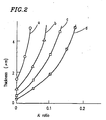
- Al t Ga 1-t N substrates (thickness: 100 ⁇ m) were formed with different Al ratios (t), and then an Al s Ga 1-s N layer (0 ⁇ s ⁇ 1) was crystal-grown on each of the substrates.
- the relationship between the Al ratio (t) and the maximum thickness of the Al s Ga 1-s N layer which can be crystal-grown without crack generation was examined. The generation of cracks was determined by a surface observation using an optical microscope. The results are shown in Figure 2 .
- the Al s Ga 1-s N layer can be crystal-grown to a greater thickness without crack generation.
- the maximum thickness of the Al 0.15 Ga 0.05 N layer which can be crystal-grown without crack generation is 0.5 ⁇ m.
- the maximum thickness of the Al 0.15 Ga 0.85 N layer which can be crystal-grown without crack generation is 3 ⁇ m.
- the upper limit of the Al ratio, s, at which the Al s Ga 1-s N layer can be grown on a substrate formed of Al 0.05 Ga 0.95 N to a thickness of 1 ⁇ m without generating cracks is about 0.2. Accordingly, the difference in the Al ratio, s, between the Al 0.05 Ga 0.95 N substrate and the Al s Ga 1-s N layer is about 0.15.
- an Al 0.15 Ga 0.85 N layer was formed on each of a GaN substrate and an Al 0.1 Ga 0.9 N substrate (thickness: 100 ⁇ m each).
- the Al 0.15 Ga 0.85 N layer on the GaN substrate caused cracks to be generated therein and bad a dislocation density of 10 9 cm -2 .
- the Al 0.15 Ga 0.85 N layer on the Al 0.1 Ga 0.9 N substrate did not cause cracks to be generated therein and had a dislocation density of 10 6 cm -2 .
- the Al 0.1 Ga 0.9 N substrate has a hardness greater than that of the GaN substrate and thus causes dislocations to be generated therein, and as a result, the Al 0.15 Ga 0.85 N layer is less likely to cause dislocations to be generated therein.
- the gallium nitride compound semiconductor light emitting device 100 has characteristics superior to those in the conventional device presumably for the following reasons:
- the n-type clad layer 11 and the p-type clad layer 13 provided on and above the n-type Al 0.1 Ga 0.9 N substrate 10 are allowed to have a thickness of as great as about 1.0 ⁇ m and thus have a lower dislocation density and include less cracks than those in the conventional device.
- the light emitting efficiency is improved, and the light can be effectively confined in the active layer 12 .
- the dislocation density of the gallium nitride compound semiconductor light emitting device is less. Specifically, when the thickness of the substrate is 40 ⁇ m, the dislocation density of the device is 10 5 cm -2 . This is considered to occur because when the thickness of the substrate is sufficiently small so as to cause dislocations to be generated therein, the dislocations are unlikely to be generated in the n-type clad layer and other layers provided on the substrate.
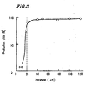
- Al 0.1 Ga 0.9 N substrates were formed with different thicknesses in order to examine the relationship between the thickness of the Al 0.1 Ga 0.9 N substrate and the production yield of the gallium nitride compound semiconductor light emitting device influenced by the cracks in the substrate.
- Figure 3 shows the results. As can be seen from Figure 3 , when the thickness of the substrate is about 20 ⁇ m or less, the production yield is lowered rapidly. Consequently, the thickness of the substrate is preferably about 20 ⁇ m or more.
- the n-type clad layer 11 and the p-type clad layer 13 can have different Al ratios from each other.
- the above description is made with regard to the gallium nitride compound semiconductor light emitting device as an example.
- the present invention is applicable to any semiconductor device including a Al x Ga 1-x N (0 ⁇ x ⁇ 1) substrate and a first semiconductor layer provided on the substrate and formed of a III-group nitride semiconductor layer containing Al.
- the difference in the Al ratio between an Al x Ga 1-x N (0 ⁇ x ⁇ 1) substrate and a first semiconductor layer formed of a III-group nitride semiconductor containing Al is less than about 0.15. Due to such a ratio, the differences in the lattice constant and in the thermal expansion coefficient of the substrate and the first semiconductor layer can be sufficiently reduced.
- the Al x Ga 1-x N substrate has a hardness sufficiently high so as to cause dislocations or cracks to be generated therein.
- An active layer formed of a III-group nitride semiconductor having a forbidden band smaller than a forbidden band of the first semiconductor layer, can be provided on the first semiconductor layer; and a second semiconductor layer formed of a III-group nitride semiconductor containing Al and having a different conductivity type from a conductivity type of the first semiconductor layer, can be provided on the active layer.
- the light is sufficiently confined in the active layer while generation of cracks is suppressed.
- the difference in the Al ratio between the substrate and the first semiconductor layer, between the first semiconductor layer and the second semiconductor layer, and between the substrate and the second semiconductor layer can all be less than about 0.15. In such an embodiment, the generation of cracks is significantly suppressed as compared to the conventional device. This allows the thickness of each of the first semiconductor layer and the second semiconductor layer to be increased to about 0.5 ⁇ m or more.
- the differences in the Al ratio between the substrate and the first semiconductor layer, between the substrate and the second semiconductor layer, and between the first semiconductor layer and the second semiconductor layer are each about 0.05 or less, the thickness of each of an n-type clad layer and a p-type clad layer can be increased to about 1.5 ⁇ m or more. As a result, the light can be sufficiently confined in the active layer so as to improve the characteristics of the semiconductor device.
- the production yield influenced by the cracks in the substrate is prevented from being lowered.
Landscapes
- Led Devices (AREA)
- Semiconductor Lasers (AREA)
- Junction Field-Effect Transistors (AREA)
Applications Claiming Priority (2)
| Application Number | Priority Date | Filing Date | Title |
|---|---|---|---|
| JP31586298 | 1998-11-06 | ||
| JP31586298 | 1998-11-06 |
Publications (3)
| Publication Number | Publication Date |
|---|---|
| EP1003227A2 true EP1003227A2 (de) | 2000-05-24 |
| EP1003227A3 EP1003227A3 (de) | 2000-08-30 |
| EP1003227B1 EP1003227B1 (de) | 2010-01-13 |
Family
ID=18070495
Family Applications (1)
| Application Number | Title | Priority Date | Filing Date |
|---|---|---|---|
| EP99120986A Expired - Lifetime EP1003227B1 (de) | 1998-11-06 | 1999-11-04 | Halbleitervorrichtung |
Country Status (4)
| Country | Link |
|---|---|
| US (1) | US6150674A (de) |
| EP (1) | EP1003227B1 (de) |
| DE (1) | DE69941921D1 (de) |
| TW (1) | TW453004B (de) |
Families Citing this family (11)
| Publication number | Priority date | Publication date | Assignee | Title |
|---|---|---|---|---|
| US6953977B2 (en) * | 2000-02-08 | 2005-10-11 | Boston Microsystems, Inc. | Micromechanical piezoelectric device |
| US6627965B1 (en) | 2000-02-08 | 2003-09-30 | Boston Microsystems, Inc. | Micromechanical device with an epitaxial layer |
| JP2002016311A (ja) * | 2000-06-27 | 2002-01-18 | Sharp Corp | 窒化ガリウム系発光素子 |
| JP4383172B2 (ja) * | 2001-10-26 | 2009-12-16 | アンモノ・スプウカ・ジ・オグラニチョノン・オドポヴィエドニアウノシツィオン | 窒化物バルク単結晶層を用いる発光素子構造及びその製造方法 |
| KR101017657B1 (ko) | 2002-04-30 | 2011-02-25 | 크리 인코포레이티드 | 고 전압 스위칭 디바이스 및 이의 제조 방법 |
| US20060138431A1 (en) | 2002-05-17 | 2006-06-29 | Robert Dwilinski | Light emitting device structure having nitride bulk single crystal layer |
| US7112830B2 (en) * | 2002-11-25 | 2006-09-26 | Apa Enterprises, Inc. | Super lattice modification of overlying transistor |
| AU2003285769A1 (en) * | 2002-12-11 | 2004-06-30 | Ammono Sp. Z O.O. | A substrate for epitaxy and a method of preparing the same |
| JP5014804B2 (ja) * | 2004-06-11 | 2012-08-29 | アンモノ・スプウカ・ジ・オグラニチョノン・オドポヴィエドニアウノシツィオン | バルク単結晶ガリウム含有窒化物およびその用途 |
| PL371405A1 (pl) * | 2004-11-26 | 2006-05-29 | Ammono Sp.Z O.O. | Sposób wytwarzania objętościowych monokryształów metodą wzrostu na zarodku |
| JP2007080896A (ja) * | 2005-09-12 | 2007-03-29 | Sanyo Electric Co Ltd | 半導体素子 |
Family Cites Families (5)
| Publication number | Priority date | Publication date | Assignee | Title |
|---|---|---|---|---|
| DE68919408T2 (de) * | 1989-01-13 | 1995-04-20 | Toshiba Kawasaki Kk | Verbindungshalbleiter, denselben anwendendes Halbleiter-Bauelement und Herstellungsverfahren des Halbleiter-Bauelementes. |
| JP3160914B2 (ja) * | 1990-12-26 | 2001-04-25 | 豊田合成株式会社 | 窒化ガリウム系化合物半導体レーザダイオード |
| DE69431333T2 (de) * | 1993-10-08 | 2003-07-31 | Mitsubishi Cable Industries, Ltd. | GaN-Einkristall |
| JPH10173228A (ja) * | 1996-12-09 | 1998-06-26 | Ricoh Co Ltd | 化合物半導体基板および半導体発光素子 |
| JP3292083B2 (ja) * | 1997-03-11 | 2002-06-17 | 日亜化学工業株式会社 | 窒化物半導体基板の製造方法及び窒化物半導体素子の製造方法 |
-
1999
- 1999-11-04 DE DE69941921T patent/DE69941921D1/de not_active Expired - Lifetime
- 1999-11-04 EP EP99120986A patent/EP1003227B1/de not_active Expired - Lifetime
- 1999-11-04 US US09/434,005 patent/US6150674A/en not_active Expired - Lifetime
- 1999-11-05 TW TW088119357A patent/TW453004B/zh not_active IP Right Cessation
Also Published As
| Publication number | Publication date |
|---|---|
| EP1003227A3 (de) | 2000-08-30 |
| DE69941921D1 (de) | 2010-03-04 |
| TW453004B (en) | 2001-09-01 |
| US6150674A (en) | 2000-11-21 |
| EP1003227B1 (de) | 2010-01-13 |
Similar Documents
| Publication | Publication Date | Title |
|---|---|---|
| US6858877B2 (en) | Nitride semiconductor, method for manufacturing the same and nitride semiconductor device | |
| EP1184913B1 (de) | Nitridhalbleiter laserdiode | |
| US6829273B2 (en) | Nitride semiconductor layer structure and a nitride semiconductor laser incorporating a portion of same | |
| JP3988018B2 (ja) | 結晶膜、結晶基板および半導体装置 | |
| US6455877B1 (en) | III-N compound semiconductor device | |
| JP5077303B2 (ja) | 窒化ガリウム系半導体発光素子、窒化ガリウム系半導体発光素子を作製する方法、窒化ガリウム系発光ダイオード、エピタキシャルウエハ、及び窒化ガリウム系発光ダイオードを作製する方法 | |
| US6690700B2 (en) | Nitride semiconductor device | |
| JP3515974B2 (ja) | 窒化物半導体、その製造方法及び窒化物半導体素子 | |
| EP1196971B1 (de) | Nitrid-halbleiterschichtenstruktur und deren anwendung in halbleiterlasern | |
| EP1122841A1 (de) | Verfahren zur herstellung einer halbleitenden nitridvorrichtung | |
| JP3394678B2 (ja) | 半導体発光素子 | |
| JP2000232238A (ja) | 窒化物半導体発光素子及びその製造方法 | |
| JP3292083B2 (ja) | 窒化物半導体基板の製造方法及び窒化物半導体素子の製造方法 | |
| US6150674A (en) | Semiconductor device having Alx Ga1-x N (0<x<1) substrate | |
| WO2010131511A1 (ja) | Iii族窒化物半導体レーザダイオード、及びiii族窒化物半導体レーザダイオードを作製する方法 | |
| JP5310382B2 (ja) | Iii族窒化物半導体光素子、及びiii族窒化物半導体光素子を作製する方法 | |
| JP4530234B2 (ja) | 半導体発光素子 | |
| JP2000252219A (ja) | GaN基板の製造方法 | |
| JP3371830B2 (ja) | 窒化物半導体発光素子 | |
| JP2000022283A (ja) | 半導体素子、半導体素子の製造方法及び半導体基板の製造方法 | |
| JP2001308464A (ja) | 窒化物半導体素子、窒化物半導体結晶の作製方法および窒化物半導体基板 | |
| JP2012231192A (ja) | 窒化ガリウム系半導体発光素子、窒化ガリウム系半導体発光素子を作製する方法、窒化ガリウム系発光ダイオード、エピタキシャルウエハ、及び窒化ガリウム系発光ダイオードを作製する方法 | |
| JP2000332293A (ja) | Iii−v族窒化物半導体発光素子及びその製造方法 | |
| JP4439048B2 (ja) | 半導体装置 | |
| JP4363415B2 (ja) | 結晶膜、結晶基板および半導体装置 |
Legal Events
| Date | Code | Title | Description |
|---|---|---|---|
| PUAI | Public reference made under article 153(3) epc to a published international application that has entered the european phase |
Free format text: ORIGINAL CODE: 0009012 |
|
| AK | Designated contracting states |
Kind code of ref document: A2 Designated state(s): DE FR GB |
|
| AX | Request for extension of the european patent |
Free format text: AL;LT;LV;MK;RO;SI |
|
| PUAL | Search report despatched |
Free format text: ORIGINAL CODE: 0009013 |
|
| AK | Designated contracting states |
Kind code of ref document: A3 Designated state(s): AT BE CH CY DE DK ES FI FR GB GR IE IT LI LU MC NL PT SE |
|
| AX | Request for extension of the european patent |
Free format text: AL;LT;LV;MK;RO;SI |
|
| 17P | Request for examination filed |
Effective date: 20010123 |
|
| AKX | Designation fees paid |
Free format text: DE FR GB |
|
| RAP1 | Party data changed (applicant data changed or rights of an application transferred) |
Owner name: MATSUSHITA ELECTRIC INDUSTRIAL CO., LTD. |
|
| RAP1 | Party data changed (applicant data changed or rights of an application transferred) |
Owner name: MATSUSHITA ELECTRIC INDUSTRIAL CO., LTD. |
|
| RAP1 | Party data changed (applicant data changed or rights of an application transferred) |
Owner name: PANASONIC CORPORATION |
|
| GRAP | Despatch of communication of intention to grant a patent |
Free format text: ORIGINAL CODE: EPIDOSNIGR1 |
|
| RIC1 | Information provided on ipc code assigned before grant |
Ipc: H01L 29/20 20060101ALI20090615BHEP Ipc: H01S 5/323 20060101ALI20090615BHEP Ipc: H01L 33/00 20060101AFI20090615BHEP |
|
| GRAS | Grant fee paid |
Free format text: ORIGINAL CODE: EPIDOSNIGR3 |
|
| GRAA | (expected) grant |
Free format text: ORIGINAL CODE: 0009210 |
|
| AK | Designated contracting states |
Kind code of ref document: B1 Designated state(s): DE FR GB |
|
| REG | Reference to a national code |
Ref country code: GB Ref legal event code: FG4D |
|
| REF | Corresponds to: |
Ref document number: 69941921 Country of ref document: DE Date of ref document: 20100304 Kind code of ref document: P |
|
| PLBE | No opposition filed within time limit |
Free format text: ORIGINAL CODE: 0009261 |
|
| STAA | Information on the status of an ep patent application or granted ep patent |
Free format text: STATUS: NO OPPOSITION FILED WITHIN TIME LIMIT |
|
| 26N | No opposition filed |
Effective date: 20101014 |
|
| PGFP | Annual fee paid to national office [announced via postgrant information from national office to epo] |
Ref country code: DE Payment date: 20131030 Year of fee payment: 15 Ref country code: FR Payment date: 20131108 Year of fee payment: 15 Ref country code: GB Payment date: 20131030 Year of fee payment: 15 |
|
| REG | Reference to a national code |
Ref country code: DE Ref legal event code: R119 Ref document number: 69941921 Country of ref document: DE |
|
| GBPC | Gb: european patent ceased through non-payment of renewal fee |
Effective date: 20141104 |
|
| REG | Reference to a national code |
Ref country code: FR Ref legal event code: ST Effective date: 20150731 |
|
| PG25 | Lapsed in a contracting state [announced via postgrant information from national office to epo] |
Ref country code: DE Free format text: LAPSE BECAUSE OF NON-PAYMENT OF DUE FEES Effective date: 20150602 Ref country code: GB Free format text: LAPSE BECAUSE OF NON-PAYMENT OF DUE FEES Effective date: 20141104 |
|
| PG25 | Lapsed in a contracting state [announced via postgrant information from national office to epo] |
Ref country code: FR Free format text: LAPSE BECAUSE OF NON-PAYMENT OF DUE FEES Effective date: 20141201 |