EP1004973A2 - Connecteur pour carte à puce - Google Patents
Connecteur pour carte à puce Download PDFInfo
- Publication number
- EP1004973A2 EP1004973A2 EP99309272A EP99309272A EP1004973A2 EP 1004973 A2 EP1004973 A2 EP 1004973A2 EP 99309272 A EP99309272 A EP 99309272A EP 99309272 A EP99309272 A EP 99309272A EP 1004973 A2 EP1004973 A2 EP 1004973A2
- Authority
- EP
- European Patent Office
- Prior art keywords
- card
- contacts
- contact
- connector
- portions
- Prior art date
- Legal status (The legal status is an assumption and is not a legal conclusion. Google has not performed a legal analysis and makes no representation as to the accuracy of the status listed.)
- Granted
Links
Images


Classifications
-
- G—PHYSICS
- G06—COMPUTING OR CALCULATING; COUNTING
- G06K—GRAPHICAL DATA READING; PRESENTATION OF DATA; RECORD CARRIERS; HANDLING RECORD CARRIERS
- G06K7/00—Methods or arrangements for sensing record carriers, e.g. for reading patterns
- G06K7/0013—Methods or arrangements for sensing record carriers, e.g. for reading patterns by galvanic contacts, e.g. card connectors for ISO-7816 compliant smart cards or memory cards, e.g. SD card readers
- G06K7/0021—Methods or arrangements for sensing record carriers, e.g. for reading patterns by galvanic contacts, e.g. card connectors for ISO-7816 compliant smart cards or memory cards, e.g. SD card readers for reading/sensing record carriers having surface contacts
Definitions
- the present invention relates generally to an IC card connector which releasably receives a card-type information storage medium, for example, a PC card, a memory card, and an IC card (any such item will be hereinbelow referred to as "IC card").
- a card-type information storage medium for example, a PC card, a memory card, and an IC card (any such item will be hereinbelow referred to as "IC card").
- an insert and connect type connector has been commonly used.
- female contacts are provided on an IC card at one end thereof while male contacts (or pins), which engage with these female contacts, are provided in the connector.
- male contacts or pins
- the contacts of the IC card come into electrical contact with the contacts of the connector.
- a contact and connect type connector is another example.
- a plurality of flat contacts are provided on a surface of the IC card while a plurality of corresponding contacts are provided in the connector. When the IC card is inserted into a card receiving room provided in the connector, the flat contacts come into contact with these contacts of the connector.
- Such a contact and connect type connector is disclosed in U.S. Pat. No. 5,051,566.
- This connector comprises a plurality of contacts, a retaining member and a releasing member.
- Each of the contacts is provided in cantilever, extending in parallel to the direction of the insertion of an IC card, such that the contact portion of each contact is positioned in the cavity which is provided for reception of an IC card.
- the retaining member is to retain the contacts in such a condition that the contacts are elastically bent and their contact portions are positioned out of the card receiving room.
- the releasing member is to release the contacts which are held by the retaining member. This releasing action is activated by the contact and push of the front end of an IC card which is inserted into the card receiving room.
- the contacts are retained elastically bent by the retaining member, so that the contact portions are not in the card receiving room.
- the releasing member is operated to release the contacts from the retaining member.
- the contact portions of the contacts return into the card receiving room because of the resiliency of each contact and come into contact with the flat contacts of the IC card.
- the timing when the contact portions meet the flat contacts is controlled to minimize the distance one contact portion travels with respect to the other in sliding contact, thereby reducing the abrasion of both the contact members.
- An IC card connector comprises a plate-like connector housing and a plurality of contacts.
- the connector housing includes a card receiving room, into which an IC card is inserted through a card insertion slot provided at the front end of the connector housing.
- the contacts are incorporated in the connector housing and are brought into contact with the flat contacts which are provided on the lower surface of the IC card for information interchange.
- Each of the contacts comprises an anchoring portion, a connect portion, and a V-shaped arm portion.
- the anchoring portion is fixed in the connector housing at a position below the card receiving room, and the connect portion is continuous from the anchoring portion.
- the V-shaped arm portion is continuous from the connect portion and includes a first arm portion which extends obliquely forward and upward from a pivot portion located centrally in the V-shaped arm portion and a second arm portion which extends obliquely rearward and upward from the pivot portion.
- the pivot portion of the V-shaped arm portion of each contact engages with the connector housing, so the downward movement of the pivot portion is restricted.
- a contact portion which is provided at the end of the first arm portion is positioned below the card receiving room while a push portion which is provided at the end of the second arm portion is positioned in the card receiving room.
- the tip of the IC card pushes downward the push portions of the V-shaped arm portions of the contacts when the IC card is inserted into the receiving room, and the resulting rocking action of the V-shaped arm portions around the pivot portions lifts the contact portions, thereby bringing the contact portions of the contacts of the connector into electrical connection with the flat contacts of the IC card.
- the dimensions of the V-shaped arm portions can be determined appropriately to adjust the timing when the contact portions of the contacts of the connector are brought into contact with the flat contacts of the IC card. In this way, the distance which the flat contacts travel sliding on the contact portions of the connector can be minimized to reduce the wear of these contact members, thereby preventing occurrence of contact failure.
- each contact portion and a corresponding push portion which works to lift or lower the contact portion, are provided in a single body as one component, respectively, not in two separate components.
- the number of parts used for the assembly of the connector is relatively small, so the production cost of the connector can be effectively reduced.
- the contacts are retained in elastic deformation even while no IC card is inserted.
- the prior-art connector may lose reliability in the secure electrical contact between the contact portions of the connector and the flat contacts of the IC card after a long period of use.
- the IC card connector of the present invention solves this problem because the contacts are released from elastic deformation while no IC card is set in the card receiving room.
- the connect portion of each of the contacts extends from the anchoring portion obliquely forward and upward continuously to the contact portion, or at first extends from the anchoring portion rearward and then makes a U turn and extends obliquely forward and upward continuously to the contact portion.
- This design is advantageous in manufacturing because the whole contacts can be formed from one sheet of plate.
- the contacts of the connector comprise a plurality of first contacts and a plurality of second contacts.
- the connect portion of each of the first contacts extends from the anchoring portion obliquely forward and upward continuously to the contact portion
- the connect portion of each of the second contacts extends from the anchoring portion rearward and then makes a U turn and then extends obliquely forward and upward continuously to the contact portion.
- the anchoring portion and the contact portion of each second contact are placed in front of the anchoring portion and the contact portion of a corresponding first contact, and because the first arm portion of each second contact is bent laterally, the second arm portions of the first contacts and the second arm portions of the second contacts are positioned laterally interchangeably in parallel with each other, extending longitudinally. In this way, the contact portion of each first contact is aligned with the contact portion of a corresponding second contact in the longitudinal direction while the push portions of the first and second contacts are aligned in the lateral direction.
- the tip of the IC card is sandwiched between the push portions of the contacts and the connector housing when the IC card is set in the card receiving room.
- This design is preferable because the IC card is retained securely in the card receiving room.
- the reliability of electrical connection between the contact portions of the connector and the flat contacts of the IC card is relatively high. Therefore, there is no need to provide a special or extra component for the purpose of retaining the IC card in the card receiving room. This is an advantage in cost reduction.
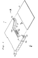
- FIG. 1 is a perspective view of an IC card and an IC card connector according to the present invention.
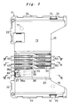
- FIG. 2 is a plan view of the IC card connector without a housing cover.
- FIG. 3 is a front view of the IC card connector, taken along line III-III in FIG. 1.
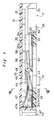
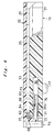
- FIG. 4 is a sectional view of the IC card connector, taken along line IV-IV in FIG. 2.
- FIG. 5 is a sectional view of the IC card connector, taken along line V-V in FIG. 2.
- FIG. 6 is a sectional view of the IC card connector, taken along line VI-VI in FIG. 2.
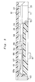
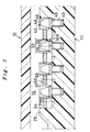
- FIG. 7 is a sectional view of the IC card connector, taken along line VII-VII in FIG. 4.
- FIGS. 8A and 8B are partial side views, showing the elastic deformation of a first contact, which deformation is caused by the insertion of an IC card, FIG. 8A showing a tip of the IC card meeting a portion of the first contact which is to be pressed downward (this portion is referred to as "push portion") and FIG. 8B showing the first contact being elastically bent and its contact portion being in contact with a flat contact of the IC card.
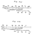
- FIGS. 9A and 9B are partial side views, showing the elastic deformation of a second contact, which deformation is caused by the insertion of the IC card, FIG. 9A showing the tip of the IC card meeting a portion of the second contact which is to be pressed downward (this portion is also referred to as "push portion") and FIG. 9B showing the second contact being elastically bent and its contact portion being in contact with a flat contact of the IC card.
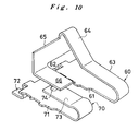
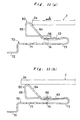
- FIG. 10 is a perspective view of first and second switch members.
- FIGS. 11A and 11B are partial side views, showing the elastic deformation of the first and second switch members, which deformation is caused by the insertion of the IC card, FIG. 11A showing the tip of the IC card meeting the first switch member and FIG. 11B showing the first switch member being elastically bent and its contact portion being in contact with the contact portion of the second switch member.
- FIG. 1 shows an IC card 2 and an IC card connector (hereinafter referred to as "connector") 1, which receives and releasably maintains this IC card 2.
- the IC card 2 incorporates an IC chip, in which various kinds of information is recorded, and a plurality of flat contacts (not shown) on the rear surface of the IC card 2.
- the flat contacts of the IC card 2 come into contact with the contacts of the connector 1 (i.e., the first and second contacts described below), thereby establishing a condition for data transmission.
- the direction indicated by arrow A is hereinafter referred to as “longitudinal direction” (the side of the root of the arrow is defined as “front side”)
- the direction of the width of the IC card 2 is hereinafter referred to as “lateral direction” (and the left hand side, in facing the connector 1 from the IC card 2, is defined as “left side”)
- the direction of the thickness of the connector 1 is hereinafter referred to as “up and down direction”.
- the connector 1 comprises a connector housing 10, which is made of an electrically insulative resin, a plurality of first contacts 40 and a plurality of second contacts 50, which are made of an electrically conductive material, and first and second switch members 60 and 70, which are also made of an electrically conductive material. These contacts and the switch members are disposed in the connector housing 10.
- the connector housing 10 comprises a main housing 11 and a housing cover 12, which is mounted on the main housing 11.
- the main housing 11 comprises a bottom wall 21, a rear wall 22, which stands upward at the rear end of the bottom wall 21, and lateral side walls 23 and 24, which stand upward at the lateral ends of the bottom wall 21.
- the bottom wall 21, the rear wall 22 and the side walls 23 and 24 of the main housing 11 together with the housing cover 12 define the card receiving room 13 with the slot 13a, which opens forward (there is an opening also at the central part of the rear wall 22).
- the main housing 11 further includes a central stage 25 and lateral side stages 26 and 27, which rise upward near the center and at the lateral sides of the bottom wall 21 inside the side walls 23 and 24, respectively.
- the upper surfaces of these stages are prepared to maintain a predetermined distance to the lower surface 12a of the housing cover 12.
- the IC card 2 is inserted in to the space defined by the upper surfaces of the side stages 26 and 27 and the lower surface of the housing cover 12 inside the card receiving room 13, so the upper surface of each side stage 26 or 27 and the lower surface 12a of the housing cover 12 forms a guide groove 28 or 29, respectively, for smooth insertion of the IC card 2.
- metal fitting anchoring slots 30 and 31, which extend upward, are provided in the lateral side walls 23 and 24, respectively, and metal fittings 14 and 15 are fixed in the metal fitting anchoring slots 30 and 31, respectively.
- two positioning pins 16 and 17 are provided protruding downward, one at a front and left location and the other at a rear and right location on the bottom wall. The metal fittings 14 and 15 and the positioning pins 16 and 17 are used to position and fix the connector 1 onto a printed circuit board (which will be described later).
- first grooves 32 in which four first contacts 40 are mounted
- second grooves 33 in which four second contacts 50 are mounted
- third grooves 34 are provided in parallel with one another in the central stage 25, each extending in the longitudinal direction.
- the first grooves 32 are positioned in the rear half of the central stage 25 while the second grooves 33 are positioned in the front half of the central stage 25.
- the center line of each of the first grooves 32 is aligned with that of a corresponding second groove 33 in the longitudinal direction
- each of the third grooves 34 is aligned on the right side (the upper side in FIG. 2) of corresponding first and second grooves 32 and 33 which are aligned in a line in the longitudinal direction.
- first and second rooms 35 and 36 are provided extending in the longitudinal direction in the rear left part of the bottom wall under the central stage 25.
- the first and second rooms 35 and 36 are used for incorporating the first and second switch members 60 and 70 in the central stage portion of the bottom wall.
- each of the first grooves 32 actually comprises an upper groove 32a and a lower groove 32b, which is positioned directly below the upper groove 32a and has a width narrower than that of the upper groove 32a.
- a first contact mounting groove 32c is provided with a width narrower than that of the lower groove 32b, at the lower part of each lower groove 32b (only in the part near the rear end of the bottom wall).
- each of the second grooves 33 has the same depth as the lower groove 32b of each first groove 32
- a second contact mounting groove 33a is provided with a width wider than that of each second groove 33 (refer to FIG. 3), at the lower part of each second groove 33 (only in the part near the front end of the bottom wall).
- each of the third grooves 34 has the same depth as each of the upper grooves 32a of the first grooves 32.
- each first contact 40 comprises an anchoring portion 41, a lead portion 42, a connect portion 43, and a V-shaped arm portion 44.
- the anchoring portion 41 is press-fit into the first contact mounting groove 32c to anchor the first contact 40.
- the lead portion 42 extends from the anchoring portion 41 downward and rearward to the rear of the bottom wall 21.
- the connect portion 43 extends obliquely from the anchoring portion 41 forward and upward and supports the V-shaped arm portion 44.
- the V-shaped arm portion 44 further includes a first arm portion 46, which extends obliquely forward and upward from a pivot portion 45, i.e., the part located at the bottom of the V, and a second arm portion 47, which extends obliquely rearward and upward from the pivot portion 45.
- a contact portion 48 which is provided at the front end of the first arm portion 46 is continuous from the connect portion 43, and the second arm portion 47 is located above the anchoring portion 41.
- the anchoring portion 41 and the lower part of the connect portion 43 are placed in the lower groove 32b while the upper part of the connect portion 43 and the V-shaped arm portion 44 are placed in the upper groove 32a, respectively.
- each first contact 40 above the anchoring portion 41 is capable of bending elastically. Because the width of the pivot portion 45 is narrower than the width of the upper groove 32a but wider than that of the lower groove 32b, the pivot portion 45 meets the bottom surface 32d of the upper groove 32a, and the further downward movement of the pivot portion 45 is restricted.
- the contact portion 48 is positioned below the card receiving room 13 while a push portion 47a, which is the horizontal rear end portion of the second arm portion 47, is positioned in the card receiving room 13.
- each second contact 50 comprises an anchoring portion 51, a lead portion 52, a connect portion 53, and a V-shaped arm portion 54.
- the anchoring portion 51 is press-fit into the second contact mounting groove 33a to anchor the second contact 50.
- the lead portion 52 extends from the anchoring portion 51 downward and forward to the front of the bottom wall 21.
- the connect portion 53 extends rearward from the anchoring portion 51 and then bends obliquely forward and upward and supports the V-shaped arm portion 54.
- the V-shaped arm portion 54 further includes a first arm portion 56, which extends obliquely forward and upward from a pivot portion 55, i.e., the part located at the bottom of the V, and a second arm portion 57, which extends obliquely rearward and upward from the pivot portion 55.
- a contact portion 58 which is provided at the front end of the first arm portion 56 is continuous from the connect portion 53, and the first arm portion 56 is located rearward with respect to and above the anchoring portion 51.
- the part of the first arm portion 56 of the V-shaped arm portion 54 from the contact portion 58 to the pivot portion 55, extends bending upward and rightward (refer to FIG. 2).
- each second contact 50 while the anchoring portion 51 and the connect portion 53 of each second contact 50 are placed in the second groove 33, the first arm portion 56 extends spanning from the second groove 33 to the third groove 34, and the pivot portion 55 and the second arm portion 57 are positioned in the third groove 34.
- the upper part of each second contact 50 above the anchoring portion 51 is capable of bending elastically.
- the pivot portion 55 meets the bottom surface 34a of the third groove 34, so the further downward movement of the pivot portion 55 is restricted.
- the contact portion 58 is positioned below the card receiving room 13 while a push portion 57a, which is the horizontal rear end portion of the second arm portion 57, is positioned in the card receiving room 13.
- each second contact 50 While the anchoring portion 51 and the contact portion 58 of each second contact 50 are positioned in front of the anchoring portion 41 and the contact portion 48 of a corresponding first contact 40, the second arm portion 47 of each first contact 40 is positioned in parallel with the second arm portion 57 of a corresponding second contact 50 because the first arm portion 56 of each second contact 50 is bent laterally.
- the second arm portions 47 of the first contacts 40 and the second arm portions 57 of the second contacts 50 are positioned interchangeably in the lateral direction.
- the first switch member 60 is placed in the first room 35, and it extends also into the second room 36.
- the first switch member 60 comprises an anchoring portion 61, a lead portion 62, a first arm portion 63, a second arm portion 64, a third arm portion 65, and a contact portion 66.
- the anchoring portion 61 is press-fit into a first switch member mounting groove 35a which is provided at the lower part of the first room 35, to fix the first switch member 60 in the main housing.
- the lead portion 62 extends from the anchoring portion 61 downward and rearward so as to be positioned at the rear of the bottom wall 21.
- the first arm portion 63 extends forward and horizontally from the anchoring portion 61, then bends upward in a U turn and extends horizontally rearward.
- the second arm portion 64 extends obliquely upward and rearward from the rear end of the first arm portion 63, and the third arm portion 65 extends downward and leftward (toward the second switch member 70) from the upper end of this second arm portion 64.
- the contact portion 66 extends horizontally forward from the lower left end of the third arm portion 65.
- a cut-out 37 is provided to open the rear parts of the first and second rooms 35 and 36 upward, so the second arm portion 64 protrudes through the cut-out 37 upward into the card receiving room 13, so the contact portion 66 is positioned in the second room 36.
- the second switch member 70 is placed in the second room 36.
- the second switch member 70 comprises an anchoring portion 71, a lead portion 72, an arm portion 73, and a contact portion 74.
- the anchoring portion 71 is press-fit into a second switch member mounting groove 36a which is provided at the lower part of the second room 36, to fix the second switch member 70 in the main housing.
- the lead portion 72 extends from the anchoring portion 71 downward and rearward so as to be positioned at the rear of the bottom wall 21.
- the arm portion 73 extends forward and horizontally from the anchoring portion 71, then bends upward in a U turn and extends horizontally rearward.
- the contact portion 74 is a convex portion which is formed on the upper surface of the arm portion 73. In the housing, the contact portion 74 of the second switch member 70 is positioned under the contact portion 66 of the first switch member 60.
- the connector 1, which is constructed as described above, is positioned on a printed circuit board (not shown) by fitting the positioning pins 16 and 17 of the connector into the holes which are provided on the printed circuit board for positioning. Then, the lead portions 42 and 52 of the first and second contacts 40 and 50 as well as the lead portions 62 and 72 of the first and second switch members 60 and 70 are surface-mounted onto corresponding terminals which are provided on the printed circuit board. Also, the lower parts (also referred to as "fixed parts") of the metal fittings 14 and 15 are surface-mounted onto corresponding pads which are provided on the printed circuit board, to fix the connector (the fixed part 14a of the metal fitting 14 is shown in FIG. 1).
- the IC card 2 is inserted through the slot 13a in the direction indicated by arrow A. During the insertion, the lateral sides of the IC card 2 are guided by the guide grooves 28 and 29 of the connector. The IC card 2 is pushed and inserted into the card receiving room 13 smoothly until the tip 2a of the IC card 2 meets the rear wall 22 of the main housing 11. During the insertion, the tip 2a of the IC card 2 hits and lowers (i.e., pushes and presses down) the push portions 47a and 57a of the first and second contacts 40 and 50 in the card receiving room 13 (refer to FIGS. 8A and 9A).
- the dimensions of the V-shaped arm portions 44 and 54 can be determined appropriately to adjust the timing when the contact portions 48 and 58 of the connector come into contact with the flat contacts of the IC card so as to minimize the distance which the flat contacts travel sliding on the contact portions 48 and 58. In this way, the wear of the contacts can be reduced to prevent occurrence of contact failure. Therefore, it is preferable that the contact portions 48 and 58 of the connector be brought into contact with the flat contacts of the IC card just before the tip 2a of the IC card 2 hits the rear wall 22 of the housing of the connector.
- each contact portion 48 or 58 and a corresponding push portion 47a or 57a which works to lift or lower the contact portion, are provided in a single body as one component, respectively. Therefore, the number of parts used for the assembly of the connector is relatively small, so the production cost of the connector is relatively small.
- the first and second contacts 40 and 50 which are experiencing an elastic deformation, have some resiliency. Therefore, the push portions 47a and 57a of the contacts of the connector push the rear end portion 2a of the IC card 2 upward onto the lower surface 12a of the housing cover 12.
- the rear end portion 2a of the IC card 2 is sandwiched between the push portions 47a and 57a of the contacts 40 and 50 and the lower surface 12a of the housing cover 12 of the connector (refer to FIGS. 8B and 9B).
- the IC card 2 is retained securely in the card receiving room 13, so the reliability of electrical connection between the contact portions 48 and 58 of the connector and the flat contacts of the IC card is relatively high. Therefore, there is no need to provide a special or extra component for the purpose of retaining the IC card 2. This is an advantage in cost reduction.
- the tip 2a of the IC card 2 hits and lowers the second arm portion 64 of the first switch member 60 (refer to FIG. 11A).
- the first switch member 60 experiences an elastic deformation, and the contact portion 66 is shifted downward and brought into contact with the contact portion 74 of the second switch member 70.
- the first switch member 60 and the second switch member 70 are connected electrically, and by this switching on, the insertion of the IC card 2 into the card receiving room 13 is detectable.
- the contact portions 66 and 74 of the first and second switch members 60 and 70 are incorporated in the main housing 11, so these contact portions are dust proof. Therefore, possibility of contact failure is relatively low.
- the contacts 40 and 50 and the switch members 60 and 70 of the connector are released form the forced elastic deformation and return to the original condition, which is the exact condition before the insertion of the IC card 2.
- the contact portions 48 and 58 of the contacts of the connector are positioned below the card receiving room 13, and the push portions 47a and 57a of the contacts are positioned in the card receiving room 13.
- the contact portions 66 and 74 of the first and second switch members 60 and 70 are separated.
- the connect portion 43 or 53 of each contact 40 or 50 is connected continuously to the contact portion 48 or 58.
- the connect portion may be connected to any portion of the V-shaped arm portion 44 or 54.
- the design used for the contacts 40 and 50 of the above embodiment, in which the connect portion of each contact is continuous to the contact portion, is advantageous in manufacturing because the whole contacts can be formed from one sheet of plate.
- two types of contacts i.e., first and second contacts 40 and 50, are used.
- an IC card connector can be constructed with only one type of contacts, either the first contacts 40 or the second contacts 50.
Landscapes
- Engineering & Computer Science (AREA)
- Artificial Intelligence (AREA)
- Computer Vision & Pattern Recognition (AREA)
- Physics & Mathematics (AREA)
- General Physics & Mathematics (AREA)
- Theoretical Computer Science (AREA)
- Coupling Device And Connection With Printed Circuit (AREA)
Applications Claiming Priority (2)
| Application Number | Priority Date | Filing Date | Title |
|---|---|---|---|
| JP33672798A JP3403098B2 (ja) | 1998-11-27 | 1998-11-27 | Icカード用コネクタ |
| JP33672798 | 1998-11-27 |
Publications (3)
| Publication Number | Publication Date |
|---|---|
| EP1004973A2 true EP1004973A2 (fr) | 2000-05-31 |
| EP1004973A3 EP1004973A3 (fr) | 2001-08-29 |
| EP1004973B1 EP1004973B1 (fr) | 2007-01-10 |
Family
ID=18302169
Family Applications (1)
| Application Number | Title | Priority Date | Filing Date |
|---|---|---|---|
| EP99309272A Expired - Lifetime EP1004973B1 (fr) | 1998-11-27 | 1999-11-22 | Connecteur pour carte à puce |
Country Status (5)
| Country | Link |
|---|---|
| US (1) | US6129571A (fr) |
| EP (1) | EP1004973B1 (fr) |
| JP (1) | JP3403098B2 (fr) |
| DE (1) | DE69934763T2 (fr) |
| TW (1) | TW446243U (fr) |
Families Citing this family (27)
| Publication number | Priority date | Publication date | Assignee | Title |
|---|---|---|---|---|
| WO2001035333A1 (fr) | 1999-11-05 | 2001-05-17 | Yamaichi Electronics Co., Ltd. | Connecteur de carte |
| JP3299945B2 (ja) | 1999-11-05 | 2002-07-08 | 山一電機株式会社 | カードコネクタ |
| JP3431553B2 (ja) * | 1999-11-05 | 2003-07-28 | 山一電機株式会社 | カードコネクタ |
| JP3635625B2 (ja) * | 1999-11-05 | 2005-04-06 | 山一電機株式会社 | カードコネクタのスイッチ構造 |
| JP3581063B2 (ja) | 1999-11-05 | 2004-10-27 | 山一電機株式会社 | カードコネクタのスイッチ構造 |
| JP3377477B2 (ja) | 1999-11-08 | 2003-02-17 | 山一電機株式会社 | カードコネクタ |
| JP3325865B2 (ja) | 1999-11-08 | 2002-09-17 | 山一電機株式会社 | カードコネクタ |
| JP3385252B2 (ja) | 1999-12-06 | 2003-03-10 | 山一電機株式会社 | カードコネクタ |
| JP3370963B2 (ja) | 1999-12-09 | 2003-01-27 | 山一電機株式会社 | カードコネクタのライトプロテクトスイッチ |
| US6508673B2 (en) | 2000-04-05 | 2003-01-21 | Mcdowell Jennifer Lyn | Low cost smart card reader, extension style, with wiping contacts |
| JP2002008778A (ja) | 2000-04-20 | 2002-01-11 | Kel Corp | カードコネクタ |
| JP3530460B2 (ja) | 2000-04-27 | 2004-05-24 | 山一電機株式会社 | カードコネクタ |
| JP4194298B2 (ja) * | 2002-05-17 | 2008-12-10 | キヤノン株式会社 | 情報記憶媒体、ユニット、プロセスカートリッジ、現像カートリッジおよび電子写真画像形成装置 |
| TW575242U (en) * | 2003-06-17 | 2004-02-01 | Molex Taiwan Ltd | Electronic card connector |
| CN100409494C (zh) * | 2003-09-25 | 2008-08-06 | 莫列斯公司 | 电子卡连接器 |
| JP2005129468A (ja) * | 2003-10-27 | 2005-05-19 | Yamaichi Electronics Co Ltd | Icカード接続用アダプタ |
| JP4210224B2 (ja) * | 2004-01-23 | 2009-01-14 | 山一電機株式会社 | 電子機器用カードコネクタ及びそれに使用されるコンタクト |
| JP4054022B2 (ja) * | 2004-03-18 | 2008-02-27 | 山一電機株式会社 | Icカード用コネクタ |
| JP2006107971A (ja) * | 2004-10-07 | 2006-04-20 | D D K Ltd | カードコネクタ |
| JP5533028B2 (ja) * | 2009-04-01 | 2014-06-25 | 山一電機株式会社 | Icカード用コネクタ |
| JP5013278B2 (ja) | 2009-08-04 | 2012-08-29 | 山一電機株式会社 | Icカード用コネクタ |
| US8177564B1 (en) | 2010-12-03 | 2012-05-15 | Yamaichi Electronics Co., Ltd. | Receptacle connector and an electrical connector using the same |
| JP5781991B2 (ja) * | 2012-08-07 | 2015-09-24 | 京セラコネクタプロダクツ株式会社 | コネクタ |
| JP5474162B2 (ja) * | 2012-11-12 | 2014-04-16 | 第一電子工業株式会社 | コンタクト及び該コンタクトを用いたコネクタ |
| JP6133706B2 (ja) * | 2013-06-21 | 2017-05-24 | 株式会社Soken | コネクタ構造 |
| JP6801563B2 (ja) * | 2017-04-13 | 2020-12-16 | 株式会社オートネットワーク技術研究所 | 雌端子 |
| JP7584935B2 (ja) | 2020-07-30 | 2024-11-18 | 株式会社ヨコオ | レセプタクル及びコネクタ |
Family Cites Families (3)
| Publication number | Priority date | Publication date | Assignee | Title |
|---|---|---|---|---|
| FR2640780A1 (fr) * | 1988-12-20 | 1990-06-22 | Cit Alcatel | Lecteur de carte a puce |
| JPH02307182A (ja) * | 1989-05-23 | 1990-12-20 | Hitachi Maxell Ltd | Icカードリーダ・ライタ |
| WO1998024045A1 (fr) * | 1996-11-27 | 1998-06-04 | The Whitaker Corporation | Connecteur pour carte a puce |
-
1998
- 1998-11-27 JP JP33672798A patent/JP3403098B2/ja not_active Expired - Lifetime
-
1999
- 1999-10-29 TW TW088218541U patent/TW446243U/zh unknown
- 1999-11-22 DE DE69934763T patent/DE69934763T2/de not_active Expired - Lifetime
- 1999-11-22 EP EP99309272A patent/EP1004973B1/fr not_active Expired - Lifetime
- 1999-11-23 US US09/448,092 patent/US6129571A/en not_active Expired - Lifetime
Also Published As
| Publication number | Publication date |
|---|---|
| JP3403098B2 (ja) | 2003-05-06 |
| DE69934763T2 (de) | 2007-10-31 |
| EP1004973B1 (fr) | 2007-01-10 |
| JP2000164271A (ja) | 2000-06-16 |
| US6129571A (en) | 2000-10-10 |
| EP1004973A3 (fr) | 2001-08-29 |
| DE69934763D1 (de) | 2007-02-22 |
| TW446243U (en) | 2001-07-11 |
Similar Documents
| Publication | Publication Date | Title |
|---|---|---|
| EP1004973B1 (fr) | Connecteur pour carte à puce | |
| US6149468A (en) | Card edge connector | |
| US5211568A (en) | Edge card connector with latch/eject mechanism | |
| JP2000506638A (ja) | スマートカード及びスマートカード用コネクタ | |
| US6655590B1 (en) | Smart card reader | |
| US6431893B1 (en) | Switch for an electrical card connector | |
| US6478630B1 (en) | Electrical card connector having polarization mechanism | |
| US5993263A (en) | Reduced mating force electrical connector | |
| US20100184334A1 (en) | Contact having increased resilience for use with electrical connector | |
| US5703346A (en) | Card receiver case | |
| US7435117B2 (en) | Card connector | |
| EP0312240A2 (fr) | Pièce de connexion électrique femelle | |
| AU4915000A (en) | One-piece electrical connector for the connection of a smart card | |
| US20090149047A1 (en) | Memory card connector with improved switch contacts for stably detection of card insertion or removal | |
| US6293805B1 (en) | Board to board connector | |
| EP1075046B1 (fr) | Dispositif de retenue pour connecteur électrique et connecteur électrique | |
| US6554627B1 (en) | Electronic card connector and method for assembling same | |
| US6361338B1 (en) | Electrical card connector | |
| US6475026B1 (en) | Flat flexible cable connector | |
| US6976880B1 (en) | Card connector | |
| US7044798B2 (en) | Card connector | |
| EP1075047A2 (fr) | Connecteur électrique pour câble plat | |
| US7686652B2 (en) | Memory card connector with improved contact arrangement | |
| US20070249232A1 (en) | Electrical connector | |
| US7377814B2 (en) | Card connector |
Legal Events
| Date | Code | Title | Description |
|---|---|---|---|
| PUAI | Public reference made under article 153(3) epc to a published international application that has entered the european phase |
Free format text: ORIGINAL CODE: 0009012 |
|
| AK | Designated contracting states |
Kind code of ref document: A2 Designated state(s): AT BE CH CY DE DK ES FI FR GB GR IE IT LI LU MC NL PT SE |
|
| AX | Request for extension of the european patent |
Free format text: AL;LT;LV;MK;RO;SI |
|
| PUAL | Search report despatched |
Free format text: ORIGINAL CODE: 0009013 |
|
| AK | Designated contracting states |
Kind code of ref document: A3 Designated state(s): AT BE CH CY DE DK ES FI FR GB GR IE IT LI LU MC NL PT SE |
|
| AX | Request for extension of the european patent |
Free format text: AL;LT;LV;MK;RO;SI |
|
| 17P | Request for examination filed |
Effective date: 20011130 |
|
| AKX | Designation fees paid |
Free format text: DE FR NL |
|
| GRAP | Despatch of communication of intention to grant a patent |
Free format text: ORIGINAL CODE: EPIDOSNIGR1 |
|
| GRAS | Grant fee paid |
Free format text: ORIGINAL CODE: EPIDOSNIGR3 |
|
| GRAA | (expected) grant |
Free format text: ORIGINAL CODE: 0009210 |
|
| AK | Designated contracting states |
Kind code of ref document: B1 Designated state(s): DE FR NL |
|
| REF | Corresponds to: |
Ref document number: 69934763 Country of ref document: DE Date of ref document: 20070222 Kind code of ref document: P |
|
| ET | Fr: translation filed | ||
| PLBE | No opposition filed within time limit |
Free format text: ORIGINAL CODE: 0009261 |
|
| STAA | Information on the status of an ep patent application or granted ep patent |
Free format text: STATUS: NO OPPOSITION FILED WITHIN TIME LIMIT |
|
| 26N | No opposition filed |
Effective date: 20071011 |
|
| PGFP | Annual fee paid to national office [announced via postgrant information from national office to epo] |
Ref country code: NL Payment date: 20071130 Year of fee payment: 9 |
|
| PG25 | Lapsed in a contracting state [announced via postgrant information from national office to epo] |
Ref country code: NL Free format text: LAPSE BECAUSE OF NON-PAYMENT OF DUE FEES Effective date: 20090601 |
|
| NLV4 | Nl: lapsed or anulled due to non-payment of the annual fee |
Effective date: 20090601 |
|
| PGFP | Annual fee paid to national office [announced via postgrant information from national office to epo] |
Ref country code: FR Payment date: 20111213 Year of fee payment: 13 |
|
| PGFP | Annual fee paid to national office [announced via postgrant information from national office to epo] |
Ref country code: DE Payment date: 20111228 Year of fee payment: 13 |
|
| REG | Reference to a national code |
Ref country code: FR Ref legal event code: ST Effective date: 20130731 |
|
| REG | Reference to a national code |
Ref country code: DE Ref legal event code: R119 Ref document number: 69934763 Country of ref document: DE Effective date: 20130601 |
|
| PG25 | Lapsed in a contracting state [announced via postgrant information from national office to epo] |
Ref country code: DE Free format text: LAPSE BECAUSE OF NON-PAYMENT OF DUE FEES Effective date: 20130601 |
|
| PG25 | Lapsed in a contracting state [announced via postgrant information from national office to epo] |
Ref country code: FR Free format text: LAPSE BECAUSE OF NON-PAYMENT OF DUE FEES Effective date: 20121130 |