EP1006389A2 - Objectif réducteur pour la microlithographie, appareil et méthode pour exposition par projection - Google Patents
Objectif réducteur pour la microlithographie, appareil et méthode pour exposition par projection Download PDFInfo
- Publication number
- EP1006389A2 EP1006389A2 EP99121205A EP99121205A EP1006389A2 EP 1006389 A2 EP1006389 A2 EP 1006389A2 EP 99121205 A EP99121205 A EP 99121205A EP 99121205 A EP99121205 A EP 99121205A EP 1006389 A2 EP1006389 A2 EP 1006389A2
- Authority
- EP
- European Patent Office
- Prior art keywords
- lens
- lens group
- refractive power
- lenses
- microlithographic projection
- Prior art date
- Legal status (The legal status is an assumption and is not a legal conclusion. Google has not performed a legal analysis and makes no representation as to the accuracy of the status listed.)
- Ceased
Links
- 238000001393 microlithography Methods 0.000 title claims description 7
- 230000009467 reduction Effects 0.000 title description 3
- 238000000034 method Methods 0.000 title 1
- 230000005499 meniscus Effects 0.000 claims description 16
- 210000001015 abdomen Anatomy 0.000 claims description 8
- 238000004519 manufacturing process Methods 0.000 claims description 6
- 241000219739 Lens Species 0.000 abstract 14
- 240000004322 Lens culinaris Species 0.000 abstract 1
- 238000012937 correction Methods 0.000 description 13
- 238000013461 design Methods 0.000 description 7
- 210000001624 hip Anatomy 0.000 description 6
- 230000004075 alteration Effects 0.000 description 4
- 230000000875 corresponding effect Effects 0.000 description 3
- 238000013507 mapping Methods 0.000 description 3
- 230000003287 optical effect Effects 0.000 description 3
- 210000001747 pupil Anatomy 0.000 description 3
- 230000008859 change Effects 0.000 description 2
- 230000007547 defect Effects 0.000 description 2
- 230000000694 effects Effects 0.000 description 2
- 239000011521 glass Substances 0.000 description 2
- 230000010354 integration Effects 0.000 description 2
- 230000000873 masking effect Effects 0.000 description 2
- 238000000206 photolithography Methods 0.000 description 2
- 206010073261 Ovarian theca cell tumour Diseases 0.000 description 1
- VYPSYNLAJGMNEJ-UHFFFAOYSA-N Silicium dioxide Chemical compound O=[Si]=O VYPSYNLAJGMNEJ-UHFFFAOYSA-N 0.000 description 1
- 238000010521 absorption reaction Methods 0.000 description 1
- 238000013459 approach Methods 0.000 description 1
- 201000009310 astigmatism Diseases 0.000 description 1
- 230000008901 benefit Effects 0.000 description 1
- 230000015572 biosynthetic process Effects 0.000 description 1
- 230000001427 coherent effect Effects 0.000 description 1
- 238000010276 construction Methods 0.000 description 1
- 238000001816 cooling Methods 0.000 description 1
- 230000008878 coupling Effects 0.000 description 1
- 238000010168 coupling process Methods 0.000 description 1
- 238000005859 coupling reaction Methods 0.000 description 1
- 230000001419 dependent effect Effects 0.000 description 1
- 230000002349 favourable effect Effects 0.000 description 1
- 238000010438 heat treatment Methods 0.000 description 1
- 238000003702 image correction Methods 0.000 description 1
- 238000003384 imaging method Methods 0.000 description 1
- 230000005855 radiation Effects 0.000 description 1
- 230000002040 relaxant effect Effects 0.000 description 1
- 208000001644 thecoma Diseases 0.000 description 1
- 238000012549 training Methods 0.000 description 1
- 238000011144 upstream manufacturing Methods 0.000 description 1
Images



Classifications
-
- G—PHYSICS
- G03—PHOTOGRAPHY; CINEMATOGRAPHY; ANALOGOUS TECHNIQUES USING WAVES OTHER THAN OPTICAL WAVES; ELECTROGRAPHY; HOLOGRAPHY
- G03F—PHOTOMECHANICAL PRODUCTION OF TEXTURED OR PATTERNED SURFACES, e.g. FOR PRINTING, FOR PROCESSING OF SEMICONDUCTOR DEVICES; MATERIALS THEREFOR; ORIGINALS THEREFOR; APPARATUS SPECIALLY ADAPTED THEREFOR
- G03F7/00—Photomechanical, e.g. photolithographic, production of textured or patterned surfaces, e.g. printing surfaces; Materials therefor, e.g. comprising photoresists; Apparatus specially adapted therefor
- G03F7/20—Exposure; Apparatus therefor
-
- G—PHYSICS
- G03—PHOTOGRAPHY; CINEMATOGRAPHY; ANALOGOUS TECHNIQUES USING WAVES OTHER THAN OPTICAL WAVES; ELECTROGRAPHY; HOLOGRAPHY
- G03F—PHOTOMECHANICAL PRODUCTION OF TEXTURED OR PATTERNED SURFACES, e.g. FOR PRINTING, FOR PROCESSING OF SEMICONDUCTOR DEVICES; MATERIALS THEREFOR; ORIGINALS THEREFOR; APPARATUS SPECIALLY ADAPTED THEREFOR
- G03F7/00—Photomechanical, e.g. photolithographic, production of textured or patterned surfaces, e.g. printing surfaces; Materials therefor, e.g. comprising photoresists; Apparatus specially adapted therefor
- G03F7/70—Microphotolithographic exposure; Apparatus therefor
- G03F7/70058—Mask illumination systems
- G03F7/70066—Size and form of the illuminated area in the mask plane, e.g. reticle masking blades or blinds
-
- G—PHYSICS
- G02—OPTICS
- G02B—OPTICAL ELEMENTS, SYSTEMS OR APPARATUS
- G02B13/00—Optical objectives specially designed for the purposes specified below
- G02B13/14—Optical objectives specially designed for the purposes specified below for use with infrared or ultraviolet radiation
- G02B13/143—Optical objectives specially designed for the purposes specified below for use with infrared or ultraviolet radiation for use with ultraviolet radiation
-
- G—PHYSICS
- G02—OPTICS
- G02B—OPTICAL ELEMENTS, SYSTEMS OR APPARATUS
- G02B13/00—Optical objectives specially designed for the purposes specified below
- G02B13/24—Optical objectives specially designed for the purposes specified below for reproducing or copying at short object distances
-
- G—PHYSICS
- G03—PHOTOGRAPHY; CINEMATOGRAPHY; ANALOGOUS TECHNIQUES USING WAVES OTHER THAN OPTICAL WAVES; ELECTROGRAPHY; HOLOGRAPHY
- G03F—PHOTOMECHANICAL PRODUCTION OF TEXTURED OR PATTERNED SURFACES, e.g. FOR PRINTING, FOR PROCESSING OF SEMICONDUCTOR DEVICES; MATERIALS THEREFOR; ORIGINALS THEREFOR; APPARATUS SPECIALLY ADAPTED THEREFOR
- G03F7/00—Photomechanical, e.g. photolithographic, production of textured or patterned surfaces, e.g. printing surfaces; Materials therefor, e.g. comprising photoresists; Apparatus specially adapted therefor
- G03F7/70—Microphotolithographic exposure; Apparatus therefor
- G03F7/70216—Mask projection systems
- G03F7/70241—Optical aspects of refractive lens systems, i.e. comprising only refractive elements
Definitions
- the generic microlithographic reduction lens according to the preamble of Claim 1 is a purely refractive high-performance lens, as it is for the high-resolution Microlithography is particularly needed in the DUV wavelength range.
- Such a lens from Tropel from 1991 is shown in Figure 16 by JH Bruning Optical Lithography - Thirty years and three orders of magnitude "SPIE, Vol 3049 , 14-27 (1997).
- Numerous variants of generic projection lenses can be found in patent applications, such as EP 0 712 019-A (US Ser. 337 647 v. 10. Nov. 1994), EP 0 717 299-A, EP 0 721 150-A, EP 0 732 605-A, EP 0 770 895-A, EP 0 803 755-A (US 5,781,278), EP 0 828 172-A .
- the object of the invention is to provide a lens type which is in the environment of the known State of the art due to high resolution with a large image field and small overall length protrudes and its image correction, especially with regard to distortion, also with different types of lighting (different degree of coherence, etc.) and with clear Stopping down (for exposures with a larger depth of field) remains stable.
- the object is achieved with a lens according to one of Claims 1, 2 and 11.
- the aperture is in the fifth lens group in the area of the third bulb of the light beam relocated. Overall, this fifth lens group and the integration of the system aperture more meaning.
- the state of the art partially the formation of the waist, specifically the first attention paid will then become largely meaningless, like that Show embodiments.
- sub-claims 3 to 9 and 12 give advantageous embodiments of fifth lens group.
- Subclaim 10 relates to the particularly advantageous dimming of the lens by individual minimization of the various image errors is achieved in each case. This will again with the design concept of the invention. Different from a lens With a fixed aperture, various large errors cannot be averaged out subtractively. The advantage is that the user can trade-off of resolution and depth of field respectively can optimize based on the application.
- a Projection exposure system according to claims 17 or 18 results in the optimal Use of these lenses and is characterized by a wide range of applications.
- the great tolerance achieved according to claim 18 is of particular importance Mapping performance against changes in lighting settings.
- the manufacturing method according to claim 19 makes of the excellent correction of Lens through flexible lighting and aperture setting at different im Manufacturing process successive exposures use.
- the individual exposures can be done on a projection exposure system with different masks, or several projection exposure systems according to the invention - also in Combination with others - can be used in a production line.
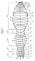
- Figures 1 to 3 and 6 for operation with one in DUV microlithography usual excimer lasers of 248, 38 nm wavelength designed and contain exclusively Quartz glass lenses. Their focal length is 1000 mm for Figures 2, 3 and 6 to 1150 mm in Figure 1 at the lower end of the customary and the feasible.
- the numeric Aperture of 0.70 (in Figures 2, 3 and 6) and 0.80 in Figure 1 is significantly above that previously known, shows the potency of the design according to the invention and allows execution microlithography with resolutions down to 0.18 ⁇ m and less under series production conditions. Until recently, such resolutions were not considered to be at all accessible with optical lithography.
- the lens is therefore suitable for a scanner with an 8 x 26 mm 2 image field.
- the lens data of the exemplary embodiment according to FIG. 1 are given in Table 1. 31 Lenses L1 to L31 and a flat plate P1 are provided. P1 serves as an easily exchangeable wafer-side end window.
- the RMS error of less than 13 m ⁇ across all image heights shows an excellent one Mapping performance.
- the lenses L1 to L5 form the first lens group LG1 with the first belly B1 of the Light beam on the back surface of lens L4.
- a negative lens L2 does the necessary Beam expansion.
- the lens group LG2 from the negative lenses L6 to L9 forms on the rear surface of the Lens L7 the first waist T1.
- Typical for this lens group LG2 are those at the waist concave menisci L6 and L9.
- the third lens group LG3 consists of the five positive lenses L10 to L14, the outer ones L10 and L14 are each formed as concave menisci on the outside, and the negative concave meniscus L15 on the image side.
- On the back surface of lens L12 is the second Belly B2 formed with the locally maximum light beam diameter.
- the fourth lens group LG4 consists of two negative lenses L16 and L17. At the The second waist T2 is formed on the rear surface of the lens L16. Here is a strong biconvex Air lens trained.
- the fifth lens group LG5 with the 14 lenses L18 to L31 is for the invention Most important objectively.
- the system diaphragm AS is arranged in front of the lens L22.
- On the front surface of the following Lens L22 is the third belly B3 with its diaphragm diameter (306.3 mm) only slightly larger light beam diameter (308.0 mm).
- the beam deflection takes place in the region of the belly B3 through a
- the majority are arranged on both sides of the aperture AS moderately stronger and thus rather thinner Positive lenses L19 to L23. This is the spherical undercorrection in this area minimized and at the same time the overall length compared to the use of fewer but stronger and thicker lenses reduced.
- the variation of the image errors when stopping down or with different lighting settings is reduced by this measure.
- the two in the divergent Lenses L19 and L20 standing in the beam path receive more refractive power.
- the L21 lenses and L22 show uniformly distributed refractive power, the beam path is between the two middle parallel.
- the lenses 21 to 23 take over a significant part of the System power with the smallest possible generation of spherical overcorrection and relax the problem of the dependency of error correction on numerical aperture and type of lighting (NA sigma problem). So are excellent Mapping properties with the most diverse lighting settings and Aperture settings accessible.
- the first lens L18 of the fifth lens group LG5 is a weakly refractive thicker concave meniscus on the object side.
- Here would be a spherical division overcorrecting air lens relaxing for the corrective effect of the following Lenses, but would disadvantageously increase the overall length.
- the lens L24 forms with the following one separated only by a thin air gap biconvex lens L25 essentially a weakly refracting thick meniscus. He balances the corresponding effect of the previous one by spherical over-correction Lenses L18 to L23.
- the split into two parts L24 and L25 in turn brings that shortest overall length. Both are the only lenses on the image side of the system diaphragm AS are concave on the object side.
- L18 stands in the divergent beam path with little stress. All rays pass through Lens surfaces largely normal.
- the meniscus L18 primarily acts as a Petzval element and presses the Petzval sum of the lens. However, this function can also be redistributed so that the thickness can be reduced.
- the split meniscus L24, L25 is convergent Beam path and is moderately to heavily loaded. He alone takes on the task of spherical over-correction of the surrounding area. In the case of a one-piece design, this requires a considerable thickness.
- the two negative menisci L29 and L30 with the final converging lens L31 are sometimes referred to in the literature as the sixth lens group.
- the correction of the sagittal oblique spherical aberration prepares when the aperture is increased special problems. Through the above measures in the aperture area, these are already mitigated but not yet resolved.
- In the field-effective area between aperture AS and Image IM is used to correct sagittal oblique spherical aberration by increasing the Individual powers of plus (L26, L27, L28, L31) and minus lenses (L29, L30) are provided.
- the means of choice is therefore the correction by compensating the higher image errors Order.
- this is also the case for the relatively large diameter of the lenses L19 to L25 responsible in the aperture area.
- the refractive power of the L29 negative lens is therefore high, three positive lenses L26 to L28 precede the distributed provision of the corresponding positive refractive power. Due to the large scope with three lenses The deflection of the lenses will make it possible to get the sine i-angle of the coma rays here keep below the value of the high numerical aperture of 0.80. The strenght Deflection of the negative meniscus L29 gives spherical in front and behind it overcorrecting airspaces.
- the correction of the image errors outside the main sections is made possible by the increased aperture very difficult.
- the correction of the refractive powers in the third lens group LG3 optimized in the area of the second abdomen B2.
- the pair of lenses L14 and L15 directs the beam into the second waist T2 and creates space-saving Just like lens L18, it makes a favorable contribution to Petzval correction.
- the positive ones Lenses L10 to L13 of the third lens group LG3 and the negative lens group LG4 are relieved of refractive power.
- the positive refractive power of L14 improves the image defects when viewed through the 45 ° section Aperture. Due to the negative refractive power of L15, the negative fourth lens group LG4 with the spherically overcorrecting lenses L16 and L17, which causes zone errors in Aperture and field are reduced.
- Two individual lenses L14, L15 are clearly preferable to a thick meniscus: on the one hand, the image error correction can be substantially improved, as shown, on the other hand, the cooling of the lenses, which is due to the slit-shaped field of scanners and the non-negligible absorption at high radiation power lens heating "known problem (especially at 193nm) is improved.
- the focal lengths are reduced to 1000 mm.
- the second embodiment of Figure 2 and Table 2 shows that the design is opposite Changes in the first two lens groups LG1 and LG2 is largely stable.
- the first lens group LG1 have the first two lenses 201 and 202 compared to FIG. 1 made a change of place.
- the second lens group LG2 there is a positive lens 207 inserted between the negative lenses 206 and 208 to 210. Training this lens group LG2 with or without a positive lens is often referred to in the prior art as shown important, so in EP 0 770 895-A (without) and EP 0 717 299-A (with).
- the fifth lens group shows the same qualitative characteristics through which reduced aperture, the lens diameters are significantly reduced.
- the third embodiment according to Figure 3 and Table 3 shows the first lens group as Example 2.
- the second lens group LG2 now shows the positive lens 308 in the middle migrated between the two negative lenses 306, 307 and 309, 310.
- the fifth lens group LG5 is now the combination of lenses L24 and L25 Figure 1 reduced to the thick meniscus 325 by one lens to 13 lenses. With this The arrangement is the same as when the meniscus is divided into the two lenses L24 and L25 an equally good imaging performance possible.
- a flat plate P1 close to the blind is also provided. This can e.g. as an apodization filter be used.
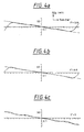
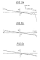
- FIG. 1 The good image error correction achieved is shown in more detail for the example in FIG. 1 become.
- Figures 4a to 4c show the sagittal transverse deviation DZS as a function of half Aperture angle DW 'for the image heights 13.6, 9.6 and 0 mm.
- Figures 5a to 5c show the corresponding meridional sections DYM.
- Table 5 gives the deviation of the distortion ⁇ V from this Vhs for various Settings of the numerical aperture NA and the degree of coherence Sigma. Ring aperture lights with the values of 0.35-0.70 and 0.50-0.85 from Sigma also taken into account. The maximum value of this deviation is 4.7 nm, mostly lying the values below 3 nm.
- the distortion is everywhere and with all settings below 10nm, even below 6nm and mostly still below. These values are related to the very high NA of 0.8 of this lens. Smaller NA can be considerably realize smaller distortions ..
- the structure largely corresponds to the example in FIG. 1.
- the air gap there is only a little curvature between the lenses 624 and 625.
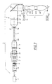
- FIG. 7 gives an overview of an example of a projection exposure system projection lens according to the invention.
- a suitable lighting system B is known for example from EP 0 747 772-A (US Ser. No. 08 / 658,605).
- Laser 1 is a common one in microlithography in the deep ultraviolet (DUV) KrF excimer laser with 248nm wavelength.
- DUV deep ultraviolet
- a beam expander 14 e.g. a mirror arrangement according to DE-A 41 24 311, is used for Coherence reduction and enlargement of the beam cross section.
- a first diffractive optical raster element 9 forms the object plane of an objective 2, in whose exit pupil is provided with a second diffractive optical raster element 8.
- a coupling optic 4 transmits the light to the entry surface 5e of a glass rod 5 the light mixes and homogenizes through multiple internal reflections.
- a reticle masking system (REMA) 51 an adjustable field diaphragm, is arranged.
- a narrow strip is formed on the reticle 7 an aspect ratio of 1: 2 to 1: 8, illuminated and by scanning the whole structured field of a chip illuminated serially.
- the lighting is extremely even and to be sharp (only in the direction perpendicular to the scanning direction).
- the design of the parts upstream of the glass rod 5, in particular the optical parts Raster elements 8 and 9 is chosen so that the inlet opening 5e not only possible homogeneous, but also with the highest possible efficiency, i.e. without essential Loss of light next to the inlet opening 5e is illuminated.
- the lens 2 is a zoom lens (movable lens 22) with integrated adjustable Axicon pair 21.
- the focal length has a triple Expansion range, so that partially coherent lighting with usual values of approx. 0.3 ⁇ ⁇ ⁇ 0.9 can be generated.
- the projection objective P according to the invention with the lens groups P1 to P5 is arranged between the reticle (mask) 7 and the wafer 9, each with a scanning device 71, 91 and the known auxiliary devices.
Landscapes
- Physics & Mathematics (AREA)
- General Physics & Mathematics (AREA)
- Optics & Photonics (AREA)
- Health & Medical Sciences (AREA)
- Toxicology (AREA)
- Lenses (AREA)
- Exposure And Positioning Against Photoresist Photosensitive Materials (AREA)
- Exposure Of Semiconductors, Excluding Electron Or Ion Beam Exposure (AREA)
Priority Applications (1)
| Application Number | Priority Date | Filing Date | Title |
|---|---|---|---|
| EP06003699A EP1686405A1 (fr) | 1998-11-30 | 1999-10-23 | Objectif de réduction microlithographique comprenant cinq groupes de lentilles |
Applications Claiming Priority (2)
| Application Number | Priority Date | Filing Date | Title |
|---|---|---|---|
| DE19855108A DE19855108A1 (de) | 1998-11-30 | 1998-11-30 | Mikrolithographisches Reduktionsobjektiv, Projektionsbelichtungsanlage und -Verfahren |
| DE19855108 | 1998-11-30 |
Related Child Applications (1)
| Application Number | Title | Priority Date | Filing Date |
|---|---|---|---|
| EP06003699A Division EP1686405A1 (fr) | 1998-11-30 | 1999-10-23 | Objectif de réduction microlithographique comprenant cinq groupes de lentilles |
Publications (2)
| Publication Number | Publication Date |
|---|---|
| EP1006389A2 true EP1006389A2 (fr) | 2000-06-07 |
| EP1006389A3 EP1006389A3 (fr) | 2002-03-20 |
Family
ID=7889445
Family Applications (2)
| Application Number | Title | Priority Date | Filing Date |
|---|---|---|---|
| EP06003699A Withdrawn EP1686405A1 (fr) | 1998-11-30 | 1999-10-23 | Objectif de réduction microlithographique comprenant cinq groupes de lentilles |
| EP99121205A Ceased EP1006389A3 (fr) | 1998-11-30 | 1999-10-23 | Objectif réducteur pour la microlithographie, appareil et méthode pour exposition par projection |
Family Applications Before (1)
| Application Number | Title | Priority Date | Filing Date |
|---|---|---|---|
| EP06003699A Withdrawn EP1686405A1 (fr) | 1998-11-30 | 1999-10-23 | Objectif de réduction microlithographique comprenant cinq groupes de lentilles |
Country Status (6)
| Country | Link |
|---|---|
| US (1) | US6349005B1 (fr) |
| EP (2) | EP1686405A1 (fr) |
| JP (1) | JP2000171706A (fr) |
| KR (1) | KR100671317B1 (fr) |
| DE (1) | DE19855108A1 (fr) |
| TW (1) | TW480347B (fr) |
Cited By (4)
| Publication number | Priority date | Publication date | Assignee | Title |
|---|---|---|---|---|
| WO2002052303A3 (fr) * | 2000-12-22 | 2002-10-31 | Zeiss Carl Semiconductor Mfg | Objectif de projection |
| US6606144B1 (en) | 1999-09-29 | 2003-08-12 | Nikon Corporation | Projection exposure methods and apparatus, and projection optical systems |
| US6674513B2 (en) | 1999-09-29 | 2004-01-06 | Nikon Corporation | Projection exposure methods and apparatus, and projection optical systems |
| US6714280B2 (en) | 2001-02-23 | 2004-03-30 | Nikon Corporation | Projection optical system, projection exposure apparatus, and projection exposure method |
Families Citing this family (35)
| Publication number | Priority date | Publication date | Assignee | Title |
|---|---|---|---|---|
| JPH1195095A (ja) | 1997-09-22 | 1999-04-09 | Nikon Corp | 投影光学系 |
| US6700645B1 (en) | 1998-01-22 | 2004-03-02 | Nikon Corporation | Projection optical system and exposure apparatus and method |
| US6635914B2 (en) * | 2000-09-08 | 2003-10-21 | Axon Technologies Corp. | Microelectronic programmable device and methods of forming and programming the same |
| EP1094350A3 (fr) | 1999-10-21 | 2001-08-16 | Carl Zeiss | Système optique de projection à lentilles |
| US6590715B2 (en) * | 1999-12-21 | 2003-07-08 | Carl-Zeiss-Stiftung | Optical projection system |
| JP2001343582A (ja) * | 2000-05-30 | 2001-12-14 | Nikon Corp | 投影光学系、当該投影光学系を備えた露光装置、及び当該露光装置を用いたマイクロデバイスの製造方法 |
| JP3413160B2 (ja) * | 2000-06-15 | 2003-06-03 | キヤノン株式会社 | 照明装置及びそれを用いた走査型露光装置 |
| DE10064685A1 (de) * | 2000-12-22 | 2002-07-04 | Zeiss Carl | Lithographieobjektiv mit einer ersten Linsengruppe, bestehend ausschließlich aus Linsen positiver Brechkraft |
| JP2002244034A (ja) | 2001-02-21 | 2002-08-28 | Nikon Corp | 投影光学系および該投影光学系を備えた露光装置 |
| JP2002323652A (ja) | 2001-02-23 | 2002-11-08 | Nikon Corp | 投影光学系,該投影光学系を備えた投影露光装置および投影露光方法 |
| DE10138847A1 (de) * | 2001-08-15 | 2003-02-27 | Zeiss Carl | Blende für eine Integratoreinheit |
| DE10143385C2 (de) | 2001-09-05 | 2003-07-17 | Zeiss Carl | Projektionsbelichtungsanlage |
| AU2003208872A1 (en) * | 2002-03-01 | 2003-09-16 | Carl Zeiss Smt Ag | Refractive projection lens with a middle part |
| US7190527B2 (en) | 2002-03-01 | 2007-03-13 | Carl Zeiss Smt Ag | Refractive projection objective |
| EP1483626A2 (fr) * | 2002-03-01 | 2004-12-08 | Carl Zeiss SMT AG | Objectif de projection a refraction |
| US7154676B2 (en) * | 2002-03-01 | 2006-12-26 | Carl Zeiss Smt A.G. | Very-high aperture projection objective |
| DE10229249A1 (de) | 2002-03-01 | 2003-09-04 | Zeiss Carl Semiconductor Mfg | Refraktives Projektionsobjektiv mit einer Taille |
| DE10210899A1 (de) * | 2002-03-08 | 2003-09-18 | Zeiss Carl Smt Ag | Refraktives Projektionsobjektiv für Immersions-Lithographie |
| DE10221386A1 (de) | 2002-05-14 | 2003-11-27 | Zeiss Carl Smt Ag | Projektionsbelichtungssystem |
| US8208198B2 (en) | 2004-01-14 | 2012-06-26 | Carl Zeiss Smt Gmbh | Catadioptric projection objective |
| JP5106858B2 (ja) | 2003-12-15 | 2012-12-26 | カール・ツァイス・エスエムティー・ゲーエムベーハー | 高開口数と平面状端面とを有する投影対物レンズ |
| US20080151365A1 (en) | 2004-01-14 | 2008-06-26 | Carl Zeiss Smt Ag | Catadioptric projection objective |
| KR101213831B1 (ko) | 2004-05-17 | 2012-12-24 | 칼 짜이스 에스엠티 게엠베하 | 중간이미지를 갖는 카타디옵트릭 투사 대물렌즈 |
| CN100370313C (zh) * | 2005-05-20 | 2008-02-20 | 清华大学 | 傅里叶变换光学系统及体全息存储傅里叶变换光学系统 |
| US7952803B2 (en) * | 2006-05-15 | 2011-05-31 | Asml Netherlands B.V. | Lithographic apparatus and device manufacturing method |
| DE102008001497A1 (de) | 2007-05-07 | 2008-11-13 | Carl Zeiss Smt Ag | Projektionsbelichtungsanlage für die Halbleiterlithographie und Subsystem einer Projektionsbelichtungsanlage |
| CN101587230B (zh) * | 2009-04-09 | 2010-12-29 | 上海微电子装备有限公司 | 一种投影物镜 |
| CN102486569B (zh) * | 2010-12-01 | 2014-06-18 | 上海微电子装备有限公司 | 一种投影物镜系统 |
| CN102540415B (zh) * | 2010-12-10 | 2014-06-18 | 上海微电子装备有限公司 | 一种投影光刻物镜 |
| CN102540416B (zh) * | 2010-12-10 | 2014-09-17 | 上海微电子装备有限公司 | 大视场大工作距投影光刻物镜 |
| CN102981249B (zh) * | 2012-09-21 | 2015-01-28 | 中国科学院光电技术研究所 | 一种投影光学系统 |
| CN107835649B (zh) | 2015-07-07 | 2021-03-23 | 高露洁-棕榄公司 | 口腔护理器具和用于口腔护理器具的单丝刷毛 |
| CN109581622B (zh) * | 2017-09-29 | 2020-12-04 | 上海微电子装备(集团)股份有限公司 | 一种投影物镜 |
| CN115542675B (zh) * | 2021-06-30 | 2025-08-12 | 上海微电子装备(集团)股份有限公司 | 投影光刻物镜及光刻机 |
| CN116954028A (zh) * | 2022-04-12 | 2023-10-27 | 上海微电子装备(集团)股份有限公司 | 光刻投影物镜及光刻机 |
Family Cites Families (32)
| Publication number | Priority date | Publication date | Assignee | Title |
|---|---|---|---|---|
| US337647A (en) | 1886-03-09 | Band-saw mill | ||
| DD299017A7 (de) | 1988-09-02 | 1992-03-26 | Jenoptik Carl Zeiss Jena Gmbh,De | Projektionsobjektiv |
| US5105075A (en) | 1988-09-19 | 1992-04-14 | Canon Kabushiki Kaisha | Projection exposure apparatus |
| SU1659955A1 (ru) | 1989-07-31 | 1991-06-30 | Конструкторское бюро точного электронного машиностроения | Проекционный объектив с увеличением - 1/5 @ |
| US5469299A (en) * | 1990-05-15 | 1995-11-21 | Olympus Optical Co., Ltd. | Objective lens system |
| JP3041939B2 (ja) | 1990-10-22 | 2000-05-15 | 株式会社ニコン | 投影レンズ系 |
| DE4124311A1 (de) | 1991-07-23 | 1993-01-28 | Zeiss Carl Fa | Anordnung zur kohaerenzreduktion und strahlformung eines laserstrahls |
| US6285443B1 (en) | 1993-12-13 | 2001-09-04 | Carl-Zeiss-Stiftung | Illuminating arrangement for a projection microlithographic apparatus |
| DE19520563A1 (de) | 1995-06-06 | 1996-12-12 | Zeiss Carl Fa | Beleuchtungseinrichtung für ein Projektions-Mikrolithographie-Gerät |
| ES1027924Y (es) | 1994-05-06 | 1995-04-01 | Medina Manuel Sierra | Chaleco de seguridad autoinchable para motoristas. |
| DE4421053A1 (de) | 1994-06-17 | 1995-12-21 | Zeiss Carl Fa | Beleuchtungseinrichtung |
| EP0687956B2 (fr) | 1994-06-17 | 2005-11-23 | Carl Zeiss SMT AG | Dispositif d'illumination |
| JPH08179204A (ja) | 1994-11-10 | 1996-07-12 | Nikon Corp | 投影光学系及び投影露光装置 |
| JP3500745B2 (ja) | 1994-12-14 | 2004-02-23 | 株式会社ニコン | 投影光学系、投影露光装置及び投影露光方法 |
| JP3454390B2 (ja) | 1995-01-06 | 2003-10-06 | 株式会社ニコン | 投影光学系、投影露光装置及び投影露光方法 |
| JP3819048B2 (ja) | 1995-03-15 | 2006-09-06 | 株式会社ニコン | 投影光学系及びそれを備えた露光装置並びに露光方法 |
| JP3402850B2 (ja) | 1995-05-09 | 2003-05-06 | キヤノン株式会社 | 投影露光装置及びそれを用いたデバイスの製造方法 |
| JP3624973B2 (ja) | 1995-10-12 | 2005-03-02 | 株式会社ニコン | 投影光学系 |
| DE19548805A1 (de) * | 1995-12-27 | 1997-07-03 | Zeiss Carl Fa | REMA-Objektiv für Mikrolithographie-Projektionsbelichtungsanlagen |
| JP3750123B2 (ja) * | 1996-04-25 | 2006-03-01 | 株式会社ニコン | 投影光学系 |
| JPH1048517A (ja) * | 1996-08-07 | 1998-02-20 | Nikon Corp | 投影光学系 |
| JPH1079345A (ja) | 1996-09-04 | 1998-03-24 | Nikon Corp | 投影光学系及び露光装置 |
| US5852490A (en) * | 1996-09-30 | 1998-12-22 | Nikon Corporation | Projection exposure method and apparatus |
| DE19653983A1 (de) * | 1996-12-21 | 1998-06-25 | Zeiss Carl Fa | REMA-Objektiv für Mikrolithographie-Projektionsbelichtungsanlagen |
| DE19818444A1 (de) * | 1997-04-25 | 1998-10-29 | Nikon Corp | Abbildungsoptik, Projektionsoptikvorrichtung und Projektionsbelichtungsverfahren |
| JP3925576B2 (ja) * | 1997-07-24 | 2007-06-06 | 株式会社ニコン | 投影光学系、該光学系を備えた露光装置、及び該装置を用いたデバイスの製造方法 |
| JPH11133301A (ja) * | 1997-08-29 | 1999-05-21 | Nikon Corp | 投影光学系、露光装置及び半導体デバイスの製造方法 |
| JPH1195095A (ja) * | 1997-09-22 | 1999-04-09 | Nikon Corp | 投影光学系 |
| JPH11214293A (ja) * | 1998-01-22 | 1999-08-06 | Nikon Corp | 投影光学系及び該光学系を備えた露光装置並びにデバイス製造方法 |
| JP2000056219A (ja) * | 1998-08-11 | 2000-02-25 | Nikon Corp | 投影光学系 |
| JP2000066075A (ja) * | 1998-08-17 | 2000-03-03 | Nikon Corp | 光学系及びその製造方法、並びに前記光学系を備えた露光装置 |
| JP2000121933A (ja) * | 1998-10-13 | 2000-04-28 | Nikon Corp | 投影光学系及びそれを備えた露光装置並びにデバイス製造方法 |
-
1998
- 1998-11-30 DE DE19855108A patent/DE19855108A1/de not_active Withdrawn
-
1999
- 1999-09-14 KR KR1019990039313A patent/KR100671317B1/ko not_active Expired - Fee Related
- 1999-10-12 US US09/416,105 patent/US6349005B1/en not_active Expired - Lifetime
- 1999-10-23 EP EP06003699A patent/EP1686405A1/fr not_active Withdrawn
- 1999-10-23 EP EP99121205A patent/EP1006389A3/fr not_active Ceased
- 1999-11-09 JP JP11317966A patent/JP2000171706A/ja active Pending
- 1999-11-09 TW TW088119509A patent/TW480347B/zh not_active IP Right Cessation
Cited By (5)
| Publication number | Priority date | Publication date | Assignee | Title |
|---|---|---|---|---|
| US6606144B1 (en) | 1999-09-29 | 2003-08-12 | Nikon Corporation | Projection exposure methods and apparatus, and projection optical systems |
| US6674513B2 (en) | 1999-09-29 | 2004-01-06 | Nikon Corporation | Projection exposure methods and apparatus, and projection optical systems |
| US6864961B2 (en) | 1999-09-29 | 2005-03-08 | Nikon Corporation | Projection exposure methods and apparatus, and projection optical systems |
| WO2002052303A3 (fr) * | 2000-12-22 | 2002-10-31 | Zeiss Carl Semiconductor Mfg | Objectif de projection |
| US6714280B2 (en) | 2001-02-23 | 2004-03-30 | Nikon Corporation | Projection optical system, projection exposure apparatus, and projection exposure method |
Also Published As
| Publication number | Publication date |
|---|---|
| EP1006389A3 (fr) | 2002-03-20 |
| US6349005B1 (en) | 2002-02-19 |
| EP1686405A1 (fr) | 2006-08-02 |
| DE19855108A1 (de) | 2000-05-31 |
| KR100671317B1 (ko) | 2007-01-18 |
| TW480347B (en) | 2002-03-21 |
| KR20000034926A (ko) | 2000-06-26 |
| JP2000171706A (ja) | 2000-06-23 |
Similar Documents
| Publication | Publication Date | Title |
|---|---|---|
| DE19855108A1 (de) | Mikrolithographisches Reduktionsobjektiv, Projektionsbelichtungsanlage und -Verfahren | |
| EP0687956B2 (fr) | Dispositif d'illumination | |
| DE69125328T2 (de) | Feldkompensierte Linse | |
| DE69531153T2 (de) | Optisches Projektionssystem mit Belichtungsgerät | |
| EP0783137B1 (fr) | Objectif REMA pour dispositifs d'illumination de microlithographie par projection | |
| EP1282011B1 (fr) | Lentille de projection réflective pour la photolithographie dans l'ultraviolet extrême | |
| DE69933973T2 (de) | Katadioptrisches optisches system und damit ausgestattete belichtungsvorrichtung | |
| DE69635725T2 (de) | Verkleinerndes optisches Ringfeldsystem mit hoher numerischer Apertur | |
| EP1855160B1 (fr) | Dispositif d'éclairage de projection, procédé d'éclairage de projection et utilisation d'un objectif de projection | |
| EP1260845A2 (fr) | Objectif de réduction catadioptrique | |
| EP1097404A1 (fr) | Objectif de projection pour la microlithographie | |
| EP1291719B1 (fr) | Appareil d'exposition par projection | |
| DE19653983A1 (de) | REMA-Objektiv für Mikrolithographie-Projektionsbelichtungsanlagen | |
| DE102009006685A1 (de) | Beleuchtungssystem für die Mikro-Lithographie | |
| EP1235112B1 (fr) | Partie d'objectif pour système d'illumination | |
| DE19833481A1 (de) | Optisches Projektionssystem, dieses verwendende Belichtungsvorrichtung und Belichtungsverfahren | |
| DE102017207582A1 (de) | Projektionsobjektiv, Projektionsbelichtungsanlage und Projektionsbelichtungsverfahren | |
| WO2016188739A1 (fr) | Système d'illumination pour une installation d'exposition par projection pour microlithographie et installation d'exposition par projection pour microlithographie comprenant un système d'illumination de ce type | |
| DE4203464B4 (de) | Katadioptrisches Reduktionsobjektiv | |
| DE102022205273B3 (de) | Beleuchtungssystem, Projektionsbelichtungsanlage und Projektionsbelichtungsverfahren | |
| EP1344112A2 (fr) | Objectif de projection | |
| DE102005024290A1 (de) | Abbildungssystem, insbesondere für eine mikrolithographische Projektionsbelichtungsanlage | |
| WO2005033800A1 (fr) | Objectif de lithographie et installation d'eclairage par projection dotee d'au moins un objectif de lithographie de ce type | |
| DE60306042T2 (de) | Relaisobjektiv in einem Beleuchtungssystem eines lithographischen Systems | |
| WO2003050587A2 (fr) | Objectif catadioptrique |
Legal Events
| Date | Code | Title | Description |
|---|---|---|---|
| PUAI | Public reference made under article 153(3) epc to a published international application that has entered the european phase |
Free format text: ORIGINAL CODE: 0009012 |
|
| AK | Designated contracting states |
Kind code of ref document: A2 Designated state(s): AT BE CH CY DE DK ES FI FR GB GR IE IT LI LU MC NL PT SE Kind code of ref document: A2 Designated state(s): DE FR GB NL |
|
| AX | Request for extension of the european patent |
Free format text: AL;LT;LV;MK;RO;SI |
|
| RIN1 | Information on inventor provided before grant (corrected) |
Inventor name: FUERTER, GERHARD Inventor name: HERKOMMER, ALOIS, DR. Inventor name: KLEM, GREGOR Inventor name: ULRICH, WILHELM Inventor name: BEIERL, HELMUT Inventor name: SCHUSTER, KARL-HEINZ |
|
| PUAL | Search report despatched |
Free format text: ORIGINAL CODE: 0009013 |
|
| AK | Designated contracting states |
Kind code of ref document: A3 Designated state(s): AT BE CH CY DE DK ES FI FR GB GR IE IT LI LU MC NL PT SE |
|
| AX | Request for extension of the european patent |
Free format text: AL;LT;LV;MK;RO;SI |
|
| 17P | Request for examination filed |
Effective date: 20020913 |
|
| 17Q | First examination report despatched |
Effective date: 20021023 |
|
| AKX | Designation fees paid |
Free format text: DE FR GB NL |
|
| RAP1 | Party data changed (applicant data changed or rights of an application transferred) |
Owner name: CARL ZEISS SMT AG |
|
| RAP1 | Party data changed (applicant data changed or rights of an application transferred) |
Owner name: CARL ZEISS SMT AG |
|
| STAA | Information on the status of an ep patent application or granted ep patent |
Free format text: STATUS: THE APPLICATION HAS BEEN REFUSED |
|
| 18R | Application refused |
Effective date: 20060317 |