EP1006519B1 - Vorrichtung zur Steuerung von Magnetköpfen und magnetisches Aufnahmegerät mit einer solchen Vorrichtung - Google Patents
Vorrichtung zur Steuerung von Magnetköpfen und magnetisches Aufnahmegerät mit einer solchen Vorrichtung Download PDFInfo
- Publication number
- EP1006519B1 EP1006519B1 EP00200441A EP00200441A EP1006519B1 EP 1006519 B1 EP1006519 B1 EP 1006519B1 EP 00200441 A EP00200441 A EP 00200441A EP 00200441 A EP00200441 A EP 00200441A EP 1006519 B1 EP1006519 B1 EP 1006519B1
- Authority
- EP
- European Patent Office
- Prior art keywords
- recording
- magnetic head
- switch elements
- current
- auxiliary coils
- Prior art date
- Legal status (The legal status is an assumption and is not a legal conclusion. Google has not performed a legal analysis and makes no representation as to the accuracy of the status listed.)
- Expired - Lifetime
Links
- 230000007423 decrease Effects 0.000 description 22
- 238000000034 method Methods 0.000 description 16
- 230000000052 comparative effect Effects 0.000 description 14
- 230000005284 excitation Effects 0.000 description 10
- 230000003287 optical effect Effects 0.000 description 10
- 230000006378 damage Effects 0.000 description 8
- 238000010586 diagram Methods 0.000 description 6
- 230000003247 decreasing effect Effects 0.000 description 5
- 230000015556 catabolic process Effects 0.000 description 3
- 230000005374 Kerr effect Effects 0.000 description 2
- 230000005415 magnetization Effects 0.000 description 2
- 239000004065 semiconductor Substances 0.000 description 2
- 238000001514 detection method Methods 0.000 description 1
- 230000000694 effects Effects 0.000 description 1
- 230000005669 field effect Effects 0.000 description 1
- 230000002401 inhibitory effect Effects 0.000 description 1
- 230000001678 irradiating effect Effects 0.000 description 1
- 230000010287 polarization Effects 0.000 description 1
- 230000007704 transition Effects 0.000 description 1
Images



Classifications
-
- G—PHYSICS
- G11—INFORMATION STORAGE
- G11B—INFORMATION STORAGE BASED ON RELATIVE MOVEMENT BETWEEN RECORD CARRIER AND TRANSDUCER
- G11B5/00—Recording by magnetisation or demagnetisation of a record carrier; Reproducing by magnetic means; Record carriers therefor
- G11B5/02—Recording, reproducing, or erasing methods; Read, write or erase circuits therefor
- G11B5/022—H-Bridge head driver circuit, the "H" configuration allowing to inverse the current direction in the head
-
- G—PHYSICS
- G11—INFORMATION STORAGE
- G11B—INFORMATION STORAGE BASED ON RELATIVE MOVEMENT BETWEEN RECORD CARRIER AND TRANSDUCER
- G11B11/00—Recording on or reproducing from the same record carrier wherein for these two operations the methods are covered by different main groups of groups G11B3/00 - G11B7/00 or by different subgroups of group G11B9/00; Record carriers therefor
- G11B11/10—Recording on or reproducing from the same record carrier wherein for these two operations the methods are covered by different main groups of groups G11B3/00 - G11B7/00 or by different subgroups of group G11B9/00; Record carriers therefor using recording by magnetic means or other means for magnetisation or demagnetisation of a record carrier, e.g. light induced spin magnetisation; Demagnetisation by thermal or stress means in the presence or not of an orienting magnetic field
- G11B11/105—Recording on or reproducing from the same record carrier wherein for these two operations the methods are covered by different main groups of groups G11B3/00 - G11B7/00 or by different subgroups of group G11B9/00; Record carriers therefor using recording by magnetic means or other means for magnetisation or demagnetisation of a record carrier, e.g. light induced spin magnetisation; Demagnetisation by thermal or stress means in the presence or not of an orienting magnetic field using a beam of light or a magnetic field for recording by change of magnetisation and a beam of light for reproducing, i.e. magneto-optical, e.g. light-induced thermomagnetic recording, spin magnetisation recording, Kerr or Faraday effect reproducing
- G11B11/10502—Recording on or reproducing from the same record carrier wherein for these two operations the methods are covered by different main groups of groups G11B3/00 - G11B7/00 or by different subgroups of group G11B9/00; Record carriers therefor using recording by magnetic means or other means for magnetisation or demagnetisation of a record carrier, e.g. light induced spin magnetisation; Demagnetisation by thermal or stress means in the presence or not of an orienting magnetic field using a beam of light or a magnetic field for recording by change of magnetisation and a beam of light for reproducing, i.e. magneto-optical, e.g. light-induced thermomagnetic recording, spin magnetisation recording, Kerr or Faraday effect reproducing characterised by the transducing operation to be executed
- G11B11/10504—Recording
- G11B11/10508—Recording by modulating only the magnetic field at the transducer
-
- G—PHYSICS
- G11—INFORMATION STORAGE
- G11B—INFORMATION STORAGE BASED ON RELATIVE MOVEMENT BETWEEN RECORD CARRIER AND TRANSDUCER
- G11B5/00—Recording by magnetisation or demagnetisation of a record carrier; Reproducing by magnetic means; Record carriers therefor
- G11B5/02—Recording, reproducing, or erasing methods; Read, write or erase circuits therefor
-
- H—ELECTRICITY
- H03—ELECTRONIC CIRCUITRY
- H03K—PULSE TECHNIQUE
- H03K17/00—Electronic switching or gating, i.e. not by contact-making and –breaking
- H03K17/51—Electronic switching or gating, i.e. not by contact-making and –breaking characterised by the components used
- H03K17/56—Electronic switching or gating, i.e. not by contact-making and –breaking characterised by the components used by the use, as active elements, of semiconductor devices
- H03K17/687—Electronic switching or gating, i.e. not by contact-making and –breaking characterised by the components used by the use, as active elements, of semiconductor devices the devices being field-effect transistors
- H03K17/6871—Electronic switching or gating, i.e. not by contact-making and –breaking characterised by the components used by the use, as active elements, of semiconductor devices the devices being field-effect transistors the output circuit comprising more than one controlled field-effect transistor
Definitions
- the present invention relates to a magnetic head drive device for modulating the magnetic field of a magnetic head in accordance with an information signal to be recorded, and a magnetic recording apparatus for recording information on a recording medium using the magnetic head drive device.
- FIG. 1 is a schematic view showing the arrangement of a magnetooptical recording apparatus adopting the magnetic field modulation method.
- a magnetooptical disk 1 as an information recording medium has a magnetooptical recording layer 1a, and is rotated by a motor 5.
- a magnetic head 2 which has an excitation coil Lh wound around a magnetic core is arranged above the upper surface of the magnetooptical disk 1, and an optical head 4 is arranged below the lower surface of the disk 1 to oppose the magnetic head 2.
- a current is supplied from a laser drive circuit 7 to a semiconductor laser 6 arranged inside the optical head 4 as a light source, and a high-power laser beam is irradiated as a very small beam spot onto the recording layer 1a of the rotating magnetooptical disk 1, thereby raising the temperature of the recording portion to a temperature equal to or higher than the Curie temperature of the recording layer.
- the magnetic head 2 is driven by a drive device 3 to generate a bias magnetic field which is modulated in correspondence with information to be recorded, and applies the generated magnetic field to the temperature raised portion of the recording layer 1a.
- the laser drive circuit 7 supplies a current smaller than that in the recording mode to the semiconductor laser 6, and a low-power laser beam is irradiated as a very small beam spot onto the recording layer 1a. Then, a sensor detects rotation of the plane of polarization of reflected light due to the recorded magnetization.
- the recording method is shifting from the mark position recording method which assigns a meaning to information at the central position of a mark to the mark edge recording method which assigns a meaning to information at the edge position of a mark.
- the edge of an information mark must be clearly recorded, and for this purpose, the reversing speed of the bias magnetic field applied from the magnetic head in the recording mode must be increased.
- a device disclosed in, e.g., Japanese Laid-Open Patent Application No. 63-94406 is known.
- Fig. 2 is a circuit diagram showing this drive device.
- the excitation coil Lh generates a bias magnetic field for the magnetic head 2
- auxiliary coils L1 and L2 are used for switching the direction of the magnetic field at high speed.
- Switch elements S1 and S2 are used for switching the direction of a current to be supplied to the excitation coil Lh
- current sources IS1 and IS2 are respectively connected to the auxiliary coils L1 and L2.
- the inductances of the auxiliary coils L1 and L2 are set to be sufficiently larger than that of the excitation main coil Lh.
- the direction of a current to be supplied to the excitation main coil Lh is switched by controlling the switch elements S1 and S2 to be alternately turned on, thereby switching the polarity of the generated magnetic field in correspondence with information to be recorded.
- the optical head 4 irradiates a laser beam having a lower intensity than that in the recording mode onto the recording layer 1a of the rotating magnetooptical disk 1, and the information signal is reproduced on the basis of reflected light by utilizing a Kerr effect of an information mark.
- both the switch elements S1 and S2 of the magnetic head drive device are turned off to stop the drive operation of the main coil Lh.
- Fig. 3A shows a binary information signal to be recorded
- Figs. 3B and 3C show the ON/OFF states of the switch elements S1 and S2, respectively.
- high level corresponds to the ON state
- low level corresponds to the OFF state.
- the switch elements S1 and S2 are alternately turned on/off in correspondence with an information signal, as shown in Figs.
- Fig. 3G shows the power of a laser beam irradiated onto the recording layer 1a. During the recording operation, a high-power laser beam is irradiated, and the laser power is switched to low power simultaneously when the recording operation is finished and the reproducing operation is started.
- Figs. 3E and 3F show the potentials at a node (a node Q1 in Fig. 2) between the switch element S1 and the auxiliary coil L2, and a node (a node Q2) between the switch element S2 and the auxiliary coil L1.
- a node Q1 in Fig. 2 shows the potentials at a node between the switch element S1 and the auxiliary coil L2, and a node (a node Q2) between the switch element S2 and the auxiliary coil L1.
- voltage pulses P1 are generated by the counter electromotive forces from the auxiliary coils L2 and L1.
- These voltage pulses P1 are inevitably generated when the switching time of the current direction of the main coil Lh is shortened, and normally have a crest value of about several tens of volts.
- one of the switch elements S1 and S2 is ON, and the current paths of the auxiliary coils L1 and L2 are not rendered nonconductive. For this reason, currents of the auxiliary coils L1 and L2 do not abruptly decrease and do not generate voltage pulses exceeding several tens of volts. For this reason, when a transistor is used as the switch element, a transistor which has a rated maximum withstand voltage of about 100 V can be selected so as not to be destroyed by the above-mentioned voltage pulses P1.
- the recording method is shifting from the mark position recording method to the mark edge recording method. In the mark edge recording method, it is required to shorten the current inversion time of the main coil of the magnetic head, and to shorten the reversal time of the magnetic field to be applied to the recording medium.
- the voltage pulse P2 becomes higher as the switching time from the ON to OFF state of the switch element becomes shorter, the voltage pulse P2 becomes still higher in the magnetic head drive circuit for the mark edge recording method.
- elements with a high withstand voltage can be used.
- such a switch element with a high withstand voltage has a large ON resistance, and increases power consumption of the drive circuit, thus posing another problem. For this reason, the switch element with a high withstand voltage is not an effective solution.
- JP-A-05174309 discloses a magnetic head driving circuit in which switching elements are provided such that excitation currents flow alternately through the coil of the magnetic head.
- DE-A-3836125 discloses a circuit for reversing a magnetic field in a magnetooptical recording/playback equipment. Diodes are provided to limit the induced voltages which occur when the switches are opened or closed.
- the present invention has been made in consideration of the conventional problems, and has as its object to provide a magnetic head drive device which can at least alleviate the problem of the destruction of the switch elements, and to provide a magnetic recording apparatus using such a magnetic head drive device.
- a magnetic head drive device comprising:
- a magnetic head and a magnetic head drive device according to the first aspect of the invention.
- Fig. 4 is a circuit diagram showing a first comparative example of a magnetic head drive device according to the present invention. Note that the same reference numerals in Fig. 4 denote the same parts as in the conventional device shown in Fig. 2.
- a main coil Lh is wound around the outer surface of a magnetic core, as shown in Fig. 1.
- the magnetic core and the main coil Lh wound around the magnetic core are arranged as a magnetic head near the surface of a magnetooptical disk 1.
- Auxiliary coils L1 and L2 are connected between the main coil and a DC power supply V, and switch elements S1 and S2 are respectively connected in series with the auxiliary coils L2 and L1.
- the switch elements S1 and S2 comprise FETs (field effect transistors).
- the auxiliary coils L1 and L2 and the switch elements S1 and S2 constitute a drive circuit for driving the magnetic head in correspondence with an information signal.
- a gate drive circuit 10 generates drive signals g1 and g2 to be applied to the gates of the switch elements S1 and S2 on the basis of an information signal d supplied from a controller (not shown).
- the gate drive circuit 10 is constituted by an inverting gate 11, OR gates 12 and 13, and AND gates 14 and 15.
- the circuit 10 generates the drive signal g1 which is in-phase with the input information signal, and the drive signal g2 which has a phase opposite to that of the drive signal g1, on the basis of the input information signal, and applies these signals to the gates of the switch elements S1 and S2.
- the operation of the gate drive circuit 10 is controlled by two control signals C1 and C2 supplied from the controller.
- the control signal C1 is a signal input to one terminal of each of the OR gates 12 and 13, and is a signal for permitting or inhibiting information recording. When the control signal C1 is at low level, information recording is permitted, and the gate drive circuit 10 generates the drive signals.
- the control signal C2 is a signal input to one terminal of each of the AND gates 14 and 15, and is a signal for instructing an operation mode of the device. In a recording mode, the control signal C2 goes to high level, and in other modes including a reproducing mode, the control signal C2 goes to low level.
- a current control circuit 16 controls a current to be supplied from the DC power supply V to the magnetic head drive circuit to be a predetermined constant current, and controls a current to be supplied to the magnetic head drive circuit to suppress generation of the above-mentioned voltage pulses upon completion of information recording.
- the current control circuit 16 comprises a resistor R1 for detecting a current, a differential amplifier 17 for detecting a current of the resistor R1 as a voltage across its two terminals, a differential amplifier 18 for comparing the output voltage from the differential amplifier 17 with a reference voltage V1 from a Zener diode D1 and outputting a control signal corresponding to the difference between the two voltages, and a transistor T1 controlled by the output signal from the differential amplifier 18.
- the Zener diode D1 breaks down, the differential amplifier 18 compares the reference voltage V1 from the Zener diode D1 and the output voltage from the differential amplifier 17 to generate an output signal corresponding to the difference between the two voltages, and the output signal is input to the base of the transistor T1.
- the reference voltage V1 of the Zener diode D1 is set in correspondence with a target value of a current to be supplied to the magnetic head drive circuit.
- the difference signal from the differential amplifier 18 increases, and control acts to decrease the current of the transistor T1.
- the difference signal from the differential amplifier 18 decreases below the target value, the difference signal from the differential amplifier 18 decreases, and feedback control is made to increase the current of the transistor T1. In this manner, the current to be supplied from the DC power supply V to the auxiliary coils L1 and L2 in the magnetic head drive circuit is controlled to a predetermined constant current by controlling the transistor T1.
- the current control circuit 16 also comprises a transistor T2.
- the transistor T2 operates to control the Zener diode to break down or to forcibly short-circuit the two terminals of the Zener diode D1.
- the transistor T2 is controlled by a control signal C3 supplied from the controller.
- the control signal C3 since the control signal C3 is at low level and the transistor T2 is set in an OFF state, the Zener diode D1 receives a current via a resistor R4 and breaks down.
- the control signal C3 goes to high level, the transistor T2 is turned on, and the Zener diode D1 is forcibly short-circuited.
- the above-mentioned magnetic head drive device of a first comparative example shown in Fig. 4 is mounted as a drive device for a magnetic head in the magnetooptical recording apparatus shown in Fig. 1. Also, each of the embodiments of drive devices for a magnetic head is mounted in the magnetooptical recording apparatus shown in Fig. 1.
- Fig. 5A shows the information signal d supplied from the controller of the magnetooptical recording apparatus to the gate drive circuit 10
- Fig. 5B shows the control signal C1 supplied from the controller of the magnetooptical recording apparatus to the gate drive circuit 10
- Fig. 5C shows the control signal C2 supplied from the controller of the magnetooptical recording apparatus to the gate drive circuit 10.
- Fig. 5D shows the control signal C3 supplied from the controller to the current control circuit 16.
- the control signal C1 is set at high level, as shown in Fig. 5B
- the control signal C2 is set at low level, as shown in Fig. 5C
- the control signal C3 is set at high level, as shown in Fig. 5D.
- the operation of the current control circuit 16 is in a stop state, and hence, the drive operation of the magnetic head is in a stop state.
- a laser beam to be irradiated is controlled to have low power.
- the control signal C2 goes to high level, as shown in Fig.
- the control signal C3 is inverted to low level, as shown in Fig. 5D.
- the control signal C1 is inverted to low level at time t 1 a predetermined period of time after the recording mode was set, as shown in Fig. 5B, and the information signal d begins to be transferred at time t 1 at which the control signal C1 is inverted to low level, as shown in Fig. 5A. Therefore, before time t 1 , the information signal is at low level, and at time t 1 at which the control signal C1 is inverted, the recording operation is started.
- the laser beam is controlled to have low power before time t 1 , and simultaneously as the recording operation is started at time t 1 , the laser beam is controlled to have high power.
- the control signal C1 is inverted to low level at time t 1 , as shown in Fig. 5B, and information recording is started.
- the gate drive circuit 10 When information is recorded, the gate drive circuit 10 generates the drive signal g1 which is in-phase with the information signal d and the drive signal g2 which has a phase opposite to that of the drive signal g1, and applies these signals to the gates of the switch elements S1 and S2.
- the switch elements S1 and S2 are alternately turned on, the current direction of the main coil Lh is switched in correspondence with the information signal, and an alternating current is supplied, as shown in Fig. 5I.
- the main coil Lh is driven in this manner, and the magnetic head generates a bias magnetic field modulated in correspondence with the information signal.
- the magnetic head is arranged near the surface of a magnetooptical disk 1, and the modulated magnetic field from the magnetic head is applied onto a recording layer 1a as a recording magnetic field.
- a constant high-power laser beam is irradiated from an optical head 4 onto the magnetooptical disk 1, and a series of information marks are recorded on the recording layer 1a by irradiation with the laser beam and application of the modulated magnetic field.
- Figs. 5J and 5K show the waveforms of potentials V Q1 and V Q2 at nodes Q1 and Q2 in Fig. 4, i.e., show the above-mentioned voltage pulses P1.
- the crest value of the voltage pulse P1 is as low as several tens of volts, as described above, and does not destroy the switch elements S1 and S2.
- the current control circuit 16 controls a current to be supplied to the magnetic head drive circuit to be constant by the above-mentioned current control operation. Therefore, even when a voltage from the DC power supply V drifts, a constant current is always supplied to the auxiliary coils L1 and L2, as shown in Figs. 5G and 5H, and the drive current of the main coil Lh is controlled to be constant.
- the control signal C1 When information recording is finished at time t 4 , the control signal C1 is inverted to high level, as shown in Fig. 5B, and the information signal d goes to low level simultaneously as the end of recording.
- the drive signals g1 and g2 from the gate drive circuit 10 go to high level, as shown in Figs. 5E and 5F, and the switch elements S1 and S2 are respectively turned on.
- the control signal C3 is inverted to high level simultaneously as the control signal C1, and the transistor T2 in the current control circuit 16 is turned on. With this operation, the Zener diode D1 is forcibly short-circuited, and the reference voltage V1 becomes nearly 0 V.
- the transistor T1 shifts from an active state to an inactive state, and a current to be supplied from the current control circuit 16 to the magnetic head drive circuit gradually decreases. Therefore, currents I L1 and I L2 of the auxiliary coils L1 and L2 gradually decrease from recording end time t 4 , as shown in Figs. 5G and 5H.
- the laser beam power is controlled to be switched from high power to low power at recording end time t 4 .
- a differential amplifier having frequency characteristics corresponding to a required current decrease speed can be selected as the differential amplifier 17 or 18.
- a low-pass filter 19 may be inserted in the control system of the current control circuit 16 so as to gradually decrease the current of the transistor T1.
- a low-pass filter may be arranged at the input side of the transistor T2 so as to gradually turn on the transistor T1.
- the decrease speed need only be sufficiently lower than the change speed upon switching of the current direction of the main coil Lh.
- the currents of the auxiliary coils L1 and L2 can decrease over the width of, e.g., the shortest pulse included in the information signal d or more.
- the control signal C2 is inverted to low level, thus ending the recording mode. In this manner, the operation mode shifts to the reproducing mode.
- the reproducing mode since the control signal C2 is inverted to low level, the drive signals g1 and g2 from the gate drive circuit 10 go to low level, as shown in Figs. 5E and 5F, and the switch elements S1 and S2 are maintained in an OFF state. Therefore, in the reproducing mode, the drive operation of the magnetic head stops.
- the reproducing mode as shown in Fig.
- a low-power laser beam is irradiated from the optical head 4 onto the magnetooptical disk 1, and light reflected by the disk 1 is detected by a photodetector in the optical head 4.
- Information is reproduced based on the detection signal from the photodetector by utilizing the Kerr effect.
- the current control circuit 16 can be prevented from being destroyed by an overvoltage. Furthermore, in this comparative example, since a current is supplied to the auxiliary coils L1 and L2 prior to information recording, as shown in Figs. 5G and 5H, a recording error caused by an insufficient current of the main coil Lh immediately after the beginning of recording can be prevented.
- the magnetic head drive device has a pair of auxiliary coils, a pair of switch elements respectively connected in series with the pair of auxiliary coils, and switch element drive means, and switches the direction of a drive current of a magnetic head arranged between nodes of the pair of auxiliary coils and the pair of switch elements in correspondence with an information signal by alternately turning on the pair of switch elements in correspondence with the information signal.
- the switch element drive means controls to maintain at least one of the pair of switch elements in an ON state for a predetermined period of time upon completion or interruption of information recording, and the device comprises current control means for gradually decreasing a current to be supplied to the pair of auxiliary coils while the switch element is in the ON state.
- the current control means comprises a current control element (transistor T1) for controlling a current to be supplied from the DC power supply to the pair of auxiliary coils.
- the current control means controls a current to be supplied to the pair of auxiliary coils to a predetermined value in the information recording mode, and controls to gradually decrease the current to be supplied to the pair of coils upon completion or interruption of information recording.
- the magnetic head drive device according to the first comparative example is used in a magnetic recording apparatus described above with reference to Fig. 1.
- the magnetic recording apparatus has a magnetic head arranged near a surface of a recording medium, and a magnetic head drive circuit which is constituted by a pair of auxiliary coils for driving the magnetic head, a pair of switch elements respectively connected in series with the pair of auxiliary coils, and switch element drive means, and modulates a magnetic field generated by the magnetic head in correspondence with an information signal to be recorded by switching a current direction of the magnetic head by alternately turning on the pair of switch elements in correspondence with the information signal, and records information by applying the modulated magnetic field of the magnetic head to the recording medium.
- a magnetic head drive circuit which is constituted by a pair of auxiliary coils for driving the magnetic head, a pair of switch elements respectively connected in series with the pair of auxiliary coils, and switch element drive means, and modulates a magnetic field generated by the magnetic head in correspondence with an information signal to be recorded by switching a current direction of the magnetic head by alternately turning on the pair of switch elements in correspondence with the information signal, and records information by applying the modulated magnetic field of the magnetic head to
- the switch element drive means controls to maintain at least one of the pair of switch elements in an ON state for a predetermined period of time upon completion or interruption of information recording
- the apparatus comprises current control means for gradually decreasing a current to be supplied to the pair of auxiliary coils while the switch element is in the ON state.
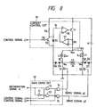
- Fig. 8 is a circuit diagram showing the first embodiment of the present invention.
- the switch elements S1 and S2 are turned off upon completion of recording, and overvoltages generated by the auxiliary coils upon completion of recording are clamped by clamp circuits, thereby protecting the switch elements.
- a clamp circuit as a series circuit of a diode D5 and a Zener diode D7 is arranged between ground and the node Q2 between the auxiliary coil L1 and the switch element S2.
- a clamp circuit as a series circuit of a diode D4 and a Zener diode D6 is arranged between ground and the node Q1 between the auxiliary coil L2 and the switch element S1.
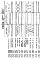
- Zener breakdown voltage v z of the Zener diodes D6 and D7 is set to have a value slightly larger than the crest value of voltage pulses P1 generated upon completion of information recording shown in Figs. 9J and 9K, since the potentials at the nodes Q1 and Q2 are lower than the Zener breakdown voltage v z during information recording, no current is supplied to the Zener diodes D6 and D7. Therefore, as shown in Figs.
- the current control circuit 16 keeps operating to supply a current to the magnetic head drive circuit.
- the switch elements S1 and S2 are OFF, the current control circuit 16 falls outside a control range as a constant current circuit, and the transistor T1 is turned on.
- the potential at the node Q3 is clamped by the power supply voltage from the DC power supply V, and even when high voltages are generated by the auxiliary coils L1 and L2 upon completion of recording, the potential at the node Q3 can be prevented from being excessively lowered below the power supply voltage, as shown in Fig.
- the diodes D4 and D5 are arranged to prevent reverse flow of currents to the Zener diodes D6 and D7.
- a clamp circuit is not limited to one using a Zener diode, but various other clamp circuits using, e.g., resistors, may be used.
- the magnetic head drive device comprises the gate drive circuit for maintaining at least one of the pair of switch elements S1 and S2 in an ON state upon completion or interruption of information recording, and the current control circuit 16 for gradually decreasing a current to be supplied to the pair of auxiliary coils L1 and L2 while the switch element is maintained in the ON state.
- the switch elements S1 and S2 are turned off, and overvoltages applied to the switch elements S1 and S2 due to the OFF operation of the switch elements are clamped by the clamp circuits (the diodes D4 and D6, and the diodes D5 and D7).
- the current control circuit 16 is kept operated to be in an ON state, thereby clamping a voltage applied to the current control circuit 16 by the power supply voltage.
- the magnetic head drive device has a pair of auxiliary coils and a pair of switch elements respectively connected in series with the pair of auxiliary coils, and switches the direction of a drive current of a magnetic head arranged between nodes of the pair of auxiliary coils and the pair of switch elements in correspondence with an information signal by alternately turning on the pair of switch elements in correspondence with the information signal.
- the device comprises switch element drive means for driving the pair of switch elements, and clamp means for clamping voltages to be applied to the pair of switch elements by counter electromotive forces from the pair of auxiliary coils.
- the pair of switch elements are turned off by the switch element drive means upon completion or interruption of information recording, and voltages, based on the counter electromotive forces of the auxiliary coils, to be applied to the switch elements due to the OFF operation of the pair of switch elements are clamped by the clamp means.
- the magnetic head drive device of the first embodiment described above is used in a magnetic recording apparatus described above with reference to Fig. 1.
- the magnetic recording apparatus has a magnetic head arranged near a surface of a recording medium, and a magnetic head drive circuit which is constituted by a pair of auxiliary coils for driving the magnetic head and a pair of switch elements respectively connected in series with the pair of auxiliary coils, and modulates a magnetic field generated by the magnetic head in correspondence with an information signal to be recorded by switching a current direction of the magnetic head by alternately turning on the pair of switch elements in correspondence with the information signal, and records information by applying the modulated magnetic field of the magnetic head to the recording medium.
- the apparatus comprises switch element drive means for driving the pair of switch elements, and clamp means for clamping voltages to be applied to the pair of switch elements due to counter electromotive forces from the pair of auxiliary coils.
- the pair of switch elements are turned off by the switch element drive means upon completion or interruption of information recording, and voltages, based on the counter electromotive forces of the auxiliary coils, to be applied to the switch elements due to the OFF operation of the pair of switch elements are clamped by the clamp means.
- a second embodiment of the present invention will be described below.
- a recording operation is temporarily stopped on the preformat region, as described above.
- the currents of the auxiliary coils can be gradually decreased, as described above. Therefore, every time recording of information for each sector is interrupted, high voltage pulses can be prevented from being generated. For this reason, even a switch element with a low withstand voltage can be used.
- this embodiment may adopt the magnetic head drive devices of the first comparative example.
- Figs. 10A to 10M are timing charts showing the operations of this embodiment, and show signals of the respective sections in correspondence with the data region and the preformat region of each sector of the recording medium.
- the control signal C1 is at low level, as shown in Fig. 10B
- the control signal C2 is at high level, as shown in Fig. 10C
- the control signal C3 is at low level, as shown in Fig. 10D.
- the gate drive circuit 10 generates the drive signals g1 and g2, as shown in Figs. 10E and 10F, in correspondence with the information signal (Fig. 10A), and drives the switch elements S1 and S2.
- the main coil Lh receives a drive current in correspondence with the information signal, as shown in Fig. 10I, and information is recorded on the data region of the recording medium by a magnetic field generated by the magnetic head and a high-power laser beam irradiated from the optical head, as shown in Fig. 10M.
- the control signal C1 is inverted to high level, as shown in Fig. 10B, and the drive signals g1 and g2 from the gate drive circuit 10 go to high level, as shown in Figs. 10E and 10F, thus maintaining the switch elements S1 and S2 in an ON state.
- the control signal C2 is kept at high level
- the control signal C3 is kept at low level. Therefore, during the preformat region period, a current is kept supplied to the auxiliary coils L1 and L2 without being cut off, as shown in Figs. 10G and 10H.
- the laser beam power is switched to low power, as shown in Fig. 10M.
- the control signal C1 is inverted to low level again, and at the same time, the laser beam power is switched to high power, thus recording information on the data region.
- the switch elements are maintained in an ON state during the preformat region period to keep supplying a current to the auxiliary coils, when recording is interrupted upon transition from the data region to the preformat region, generation of high voltages by the auxiliary coils can be completely prevented. Since the currents of the auxiliary coils do not change, overvoltages can be prevented from being generated at the node Q3, as shown in Fig. 10L, and destruction of the current control circuit 16 can be completely prevented. Furthermore, in the conventional device, since the currents of the auxiliary coils do not sufficiently rise at the beginning of recording, a recording error may often be caused by an insufficient magnetic field.
- both the switch elements S1 and S2 are maintained in an ON state during the preformat region period. In this case, at least one of the switch elements need only be maintained in an ON state.
- switch element drive means turns on at least one of the switch elements during a preformat region period to keep supplying a current to the auxiliary coils.
- the magnetic recording apparatus of each of the first and second embodiments further comprises an optical head for irradiating a light beam onto a recording medium, and records information on the recording medium by irradiation of the light beam from the optical head and application of a modulated magnetic field from the magnetic head.
- a magnetooptical recording apparatus adopting a magnetic field modulation method for recording information by irradiation of a light beam and application of a modulated magnetic field has been exemplified as an information recording apparatus.
- the present invention is not limited to this but may be applied to a magnetic recording apparatus for recording information by applying a modulated magnetic field.
- the present invention can provide the following effects.
Claims (4)
- Vorrichtung zur Steuerung von Magnetköpfen, mit:wobei die Klammerspannung einen höheren Pegel aufweist als die Spannungspulse (P1), die aufgrund von elektromotorischen Gegenkräften durch das Paar von Zusatzspulen (L1, L2) während einer Informationsaufzeichnung erzeugt werden, und einen niedrigeren Pegel aufweist als die Spannungspulse (P2), die aufgrund von elektromotorischen Gegenkräften durch das Paar von Zusatzspulen (L1, L2) nach Vollendung oder bei Unterbrechung einer Informationsaufzeichnung erzeugt werden.einem Paar von Zusatzspulen (L1, L2),einem Paar von Schaltelementen (S1, S2), die jeweils mit einer der Zusatzspulen (L1, L2) in Serie geschaltet sind,einem Magnetkopf (Lh ), der zwischen Knoten (Q1, Q2) des Paares von Zusatzspulen (L1, L2) und dem Paar von Schaltelementen (S1, S2) geschaltet ist, undeinem Schaltelement-Ansteuermittel (10) zum Steuern des Paares von Schaltelementen (S1, S2), wobei das Schaltelement-Ansteuermittel das Paar von Schaltelementen nach Vollendung einer Informationsaufzeichnung durch den Magnetkopf in einen AUS-Zustand setzt,dabei ist die Vorrichtung dadurch gekennzeichnet, dasssie ein Klammermittel zum Klammern von Spannungen, die an jedes der Schaltelemente (S1, S2) anzulegen sind, durch Verwenden einer vorbestimmten Klammerspannung aufweist,
- Vorrichtung nach Anspruch 1, wobei das Klammermittel Dioden (D4, D5, D6, D7) aufweist.
- Magnetaufzeichnungsgerät, mit:einem Magnetkopf (Lh ), undeiner Magnetkopfansteuervorrichtung zum Zuführen von Strom zum Magnetkopf (Lh ), wobei die Magnetkopfansteuervorrichtung eine Vorrichtung nach Anspruch 1 oder 2 ist.
- Gerät nach Anspruch 3, wobei das Magnetaufzeichnungsgerät ein magnetooptisches Aufzeichnungsgerät ist.
Applications Claiming Priority (3)
| Application Number | Priority Date | Filing Date | Title |
|---|---|---|---|
| JP05213550A JP3107265B2 (ja) | 1993-08-06 | 1993-08-06 | 磁気ヘッド駆動装置及び磁気記録装置 |
| JP21355093 | 1993-08-06 | ||
| EP94305826A EP0637822B1 (de) | 1993-08-06 | 1994-08-05 | Vorrichtung zur Steuerung von Magnetköpfen und magnetisches Aufnahmegerät mit einer solchen Vorrichtung |
Related Parent Applications (1)
| Application Number | Title | Priority Date | Filing Date |
|---|---|---|---|
| EP94305826A Division EP0637822B1 (de) | 1993-08-06 | 1994-08-05 | Vorrichtung zur Steuerung von Magnetköpfen und magnetisches Aufnahmegerät mit einer solchen Vorrichtung |
Publications (3)
| Publication Number | Publication Date |
|---|---|
| EP1006519A2 EP1006519A2 (de) | 2000-06-07 |
| EP1006519A3 EP1006519A3 (de) | 2000-10-11 |
| EP1006519B1 true EP1006519B1 (de) | 2004-07-07 |
Family
ID=16641062
Family Applications (2)
| Application Number | Title | Priority Date | Filing Date |
|---|---|---|---|
| EP00200441A Expired - Lifetime EP1006519B1 (de) | 1993-08-06 | 1994-08-05 | Vorrichtung zur Steuerung von Magnetköpfen und magnetisches Aufnahmegerät mit einer solchen Vorrichtung |
| EP94305826A Expired - Lifetime EP0637822B1 (de) | 1993-08-06 | 1994-08-05 | Vorrichtung zur Steuerung von Magnetköpfen und magnetisches Aufnahmegerät mit einer solchen Vorrichtung |
Family Applications After (1)
| Application Number | Title | Priority Date | Filing Date |
|---|---|---|---|
| EP94305826A Expired - Lifetime EP0637822B1 (de) | 1993-08-06 | 1994-08-05 | Vorrichtung zur Steuerung von Magnetköpfen und magnetisches Aufnahmegerät mit einer solchen Vorrichtung |
Country Status (4)
| Country | Link |
|---|---|
| US (1) | US5574702A (de) |
| EP (2) | EP1006519B1 (de) |
| JP (1) | JP3107265B2 (de) |
| DE (2) | DE69426218T2 (de) |
Families Citing this family (10)
| Publication number | Priority date | Publication date | Assignee | Title |
|---|---|---|---|---|
| KR0183824B1 (ko) * | 1995-08-16 | 1999-04-15 | 김광호 | 자기기록장치 및 방법 |
| JPH1097702A (ja) * | 1996-09-20 | 1998-04-14 | Toshiba Corp | 磁気ディスク装置及び同装置に適用するデータ再生回路 |
| US5852526A (en) * | 1996-09-25 | 1998-12-22 | Silicon Systems, Inc. | Low bias voltage write driver using a low bias voltage to reduce the risk of head arcing |
| JPH1186203A (ja) * | 1997-09-03 | 1999-03-30 | Canon Inc | 磁気ヘッド駆動装置及び光磁気記録装置 |
| DE19930513A1 (de) | 1999-07-05 | 2001-01-11 | Thomson Brandt Gmbh | Gerät zum Abtasten optischer Aufzeichnungsträger |
| JP2001176142A (ja) | 1999-12-16 | 2001-06-29 | Canon Inc | 磁気ヘッド駆動回路及び光磁気記録装置 |
| US6847500B2 (en) * | 2001-09-06 | 2005-01-25 | Hitachi Global Storage Technologies Netherlands B.V. | Methods and apparatus for gradually decreasing supply current demand in arm electronics for write-to-read transitions |
| US7085089B2 (en) * | 2003-04-01 | 2006-08-01 | Agere Systems Inc. | System and method for reducing circumferential transition incoherence in servowriting operations and magnetic disk drive incorporating the same |
| WO2005065735A1 (en) | 2003-12-31 | 2005-07-21 | Boston Scientific Limited | Medical device with varying physical properties and method for forming same |
| US7092185B2 (en) * | 2004-07-08 | 2006-08-15 | Agere Systems Inc. | Write gate timing for a servo bank |
Citations (1)
| Publication number | Priority date | Publication date | Assignee | Title |
|---|---|---|---|---|
| DE3836125A1 (de) * | 1988-10-22 | 1990-05-03 | Thomson Brandt Gmbh | Schaltungsanordnung zur umkehrung eines magnetfeldes |
Family Cites Families (11)
| Publication number | Priority date | Publication date | Assignee | Title |
|---|---|---|---|---|
| JPH0743805B2 (ja) * | 1986-10-07 | 1995-05-15 | ソニー株式会社 | 磁気ヘツド駆動回路 |
| JPS63244402A (ja) * | 1987-03-31 | 1988-10-11 | Sony Corp | 記録用磁界発生回路 |
| US5107151A (en) * | 1989-08-22 | 1992-04-21 | Unique Mobility, Inc. | Switching circuit employing electronic devices in series with an inductor to avoid commutation breakdown and extending the current range of switching circuits by using igbt devices in place of mosfets |
| JP3097088B2 (ja) * | 1989-12-27 | 2000-10-10 | ソニー株式会社 | 磁気ヘッド駆動回路 |
| DE4022410A1 (de) * | 1990-07-13 | 1992-01-16 | Thomson Brandt Gmbh | Schaltungsanordnung zur umkehrung eines magnetfeldes |
| JP2795757B2 (ja) * | 1991-06-21 | 1998-09-10 | シャープ株式会社 | 磁気ヘッド駆動回路 |
| JP2889411B2 (ja) * | 1991-10-31 | 1999-05-10 | キヤノン株式会社 | 磁気ヘッド駆動装置 |
| JP2871924B2 (ja) * | 1991-12-19 | 1999-03-17 | キヤノン株式会社 | 磁気ヘッド駆動装置 |
| JP2859766B2 (ja) * | 1991-12-24 | 1999-02-24 | シャープ株式会社 | 磁気ヘッド駆動回路 |
| JP2976697B2 (ja) * | 1992-05-29 | 1999-11-10 | 松下電器産業株式会社 | 光磁気ディスク用変調磁界発生装置 |
| JP3098896B2 (ja) * | 1992-06-23 | 2000-10-16 | キヤノン株式会社 | 光磁気記録装置 |
-
1993
- 1993-08-06 JP JP05213550A patent/JP3107265B2/ja not_active Expired - Fee Related
-
1994
- 1994-08-05 DE DE69426218T patent/DE69426218T2/de not_active Expired - Lifetime
- 1994-08-05 EP EP00200441A patent/EP1006519B1/de not_active Expired - Lifetime
- 1994-08-05 US US08/286,331 patent/US5574702A/en not_active Expired - Lifetime
- 1994-08-05 EP EP94305826A patent/EP0637822B1/de not_active Expired - Lifetime
- 1994-08-05 DE DE69433890T patent/DE69433890T2/de not_active Expired - Lifetime
Patent Citations (1)
| Publication number | Priority date | Publication date | Assignee | Title |
|---|---|---|---|---|
| DE3836125A1 (de) * | 1988-10-22 | 1990-05-03 | Thomson Brandt Gmbh | Schaltungsanordnung zur umkehrung eines magnetfeldes |
Also Published As
| Publication number | Publication date |
|---|---|
| DE69426218D1 (de) | 2000-12-07 |
| EP0637822B1 (de) | 2000-11-02 |
| DE69433890D1 (de) | 2004-08-12 |
| DE69426218T2 (de) | 2001-04-26 |
| DE69433890T2 (de) | 2005-06-30 |
| EP0637822A3 (de) | 1995-08-02 |
| EP1006519A3 (de) | 2000-10-11 |
| US5574702A (en) | 1996-11-12 |
| JPH0757202A (ja) | 1995-03-03 |
| EP0637822A2 (de) | 1995-02-08 |
| JP3107265B2 (ja) | 2000-11-06 |
| EP1006519A2 (de) | 2000-06-07 |
Similar Documents
| Publication | Publication Date | Title |
|---|---|---|
| JP3211999B2 (ja) | 光磁気記録装置 | |
| EP1006519B1 (de) | Vorrichtung zur Steuerung von Magnetköpfen und magnetisches Aufnahmegerät mit einer solchen Vorrichtung | |
| JP2598312B2 (ja) | 光磁気記録装置及びそのような光磁気記録装置に用いる駆動回路 | |
| EP0540275B1 (de) | Schaltungsvorrichtung zur Steuerung eines magnetischen Kopfs | |
| US5586091A (en) | Magnetooptical recording apparatus including a control circuit for driving a switch element between on and off states in accordance with an error detection | |
| JPH04372701A (ja) | 磁気ヘッド駆動回路 | |
| EP0855704B1 (de) | Magnetkopfantriebsvorrichtung | |
| JPH06333202A (ja) | 磁気ヘッド駆動装置および光磁気記録装置 | |
| US5377172A (en) | Modulated magnetic field generation circuit for magneto-optical disks | |
| JPH03157839A (ja) | 光磁気ディスク用高周波変調磁界発生装置 | |
| US5331477A (en) | Low voltage, constant current magnetic transducer drive system for digital recording | |
| JPH0469802A (ja) | 磁気変調コイル駆動回路 | |
| JP3144601B2 (ja) | 磁気ヘツド駆動装置 | |
| JP2880743B2 (ja) | 光磁気記録用外部印加磁界供給装置 | |
| JPH05128404A (ja) | 光磁気記録用変調磁界発生装置および光磁気記録装置 | |
| JP3898209B2 (ja) | 光情報記録方式 | |
| JPH08167188A (ja) | 半導体レーザ制御回路 | |
| JP2868101B2 (ja) | 磁気ヘッド駆動装置 | |
| JPH04255945A (ja) | 光磁気情報記録再生装置 | |
| JPH06131609A (ja) | 磁気ヘッド駆動装置 | |
| JPH07114703A (ja) | 磁気ヘッド駆動回路 | |
| JPH0727657B2 (ja) | 光ディスク装置の光源駆動装置 | |
| JPH11353684A (ja) | 半導体レーザ制御装置 | |
| US20010015938A1 (en) | Magnetic head drive circuit and magneto-optical recording device | |
| JPH07169002A (ja) | 磁気ヘッド駆動回路 |
Legal Events
| Date | Code | Title | Description |
|---|---|---|---|
| PUAI | Public reference made under article 153(3) epc to a published international application that has entered the european phase |
Free format text: ORIGINAL CODE: 0009012 |
|
| AC | Divisional application: reference to earlier application |
Ref document number: 637822 Country of ref document: EP |
|
| AK | Designated contracting states |
Kind code of ref document: A2 Designated state(s): DE ES FR GB IT NL |
|
| PUAL | Search report despatched |
Free format text: ORIGINAL CODE: 0009013 |
|
| AK | Designated contracting states |
Kind code of ref document: A3 Designated state(s): DE ES FR GB IT NL |
|
| 17P | Request for examination filed |
Effective date: 20010312 |
|
| AKX | Designation fees paid |
Free format text: DE ES FR GB IT NL |
|
| 17Q | First examination report despatched |
Effective date: 20020418 |
|
| GRAP | Despatch of communication of intention to grant a patent |
Free format text: ORIGINAL CODE: EPIDOSNIGR1 |
|
| GRAS | Grant fee paid |
Free format text: ORIGINAL CODE: EPIDOSNIGR3 |
|
| GRAA | (expected) grant |
Free format text: ORIGINAL CODE: 0009210 |
|
| AC | Divisional application: reference to earlier application |
Ref document number: 0637822 Country of ref document: EP Kind code of ref document: P |
|
| AK | Designated contracting states |
Kind code of ref document: B1 Designated state(s): DE ES FR GB IT NL |
|
| PG25 | Lapsed in a contracting state [announced via postgrant information from national office to epo] |
Ref country code: IT Free format text: LAPSE BECAUSE OF FAILURE TO SUBMIT A TRANSLATION OF THE DESCRIPTION OR TO PAY THE FEE WITHIN THE PRESCRIBED TIME-LIMIT;WARNING: LAPSES OF ITALIAN PATENTS WITH EFFECTIVE DATE BEFORE 2007 MAY HAVE OCCURRED AT ANY TIME BEFORE 2007. THE CORRECT EFFECTIVE DATE MAY BE DIFFERENT FROM THE ONE RECORDED. Effective date: 20040707 Ref country code: NL Free format text: LAPSE BECAUSE OF FAILURE TO SUBMIT A TRANSLATION OF THE DESCRIPTION OR TO PAY THE FEE WITHIN THE PRESCRIBED TIME-LIMIT Effective date: 20040707 Ref country code: FR Free format text: LAPSE BECAUSE OF FAILURE TO SUBMIT A TRANSLATION OF THE DESCRIPTION OR TO PAY THE FEE WITHIN THE PRESCRIBED TIME-LIMIT Effective date: 20040707 |
|
| REG | Reference to a national code |
Ref country code: GB Ref legal event code: FG4D |
|
| REF | Corresponds to: |
Ref document number: 69433890 Country of ref document: DE Date of ref document: 20040812 Kind code of ref document: P |
|
| PG25 | Lapsed in a contracting state [announced via postgrant information from national office to epo] |
Ref country code: ES Free format text: LAPSE BECAUSE OF FAILURE TO SUBMIT A TRANSLATION OF THE DESCRIPTION OR TO PAY THE FEE WITHIN THE PRESCRIBED TIME-LIMIT Effective date: 20041018 |
|
| NLV1 | Nl: lapsed or annulled due to failure to fulfill the requirements of art. 29p and 29m of the patents act | ||
| PLBE | No opposition filed within time limit |
Free format text: ORIGINAL CODE: 0009261 |
|
| STAA | Information on the status of an ep patent application or granted ep patent |
Free format text: STATUS: NO OPPOSITION FILED WITHIN TIME LIMIT |
|
| 26N | No opposition filed |
Effective date: 20050408 |
|
| EN | Fr: translation not filed | ||
| PGFP | Annual fee paid to national office [announced via postgrant information from national office to epo] |
Ref country code: DE Payment date: 20090831 Year of fee payment: 16 Ref country code: GB Payment date: 20090827 Year of fee payment: 16 |
|
| GBPC | Gb: european patent ceased through non-payment of renewal fee |
Effective date: 20100805 |
|
| REG | Reference to a national code |
Ref country code: DE Ref legal event code: R119 Ref document number: 69433890 Country of ref document: DE Effective date: 20110301 |
|
| PG25 | Lapsed in a contracting state [announced via postgrant information from national office to epo] |
Ref country code: DE Free format text: LAPSE BECAUSE OF NON-PAYMENT OF DUE FEES Effective date: 20110301 |
|
| PG25 | Lapsed in a contracting state [announced via postgrant information from national office to epo] |
Ref country code: GB Free format text: LAPSE BECAUSE OF NON-PAYMENT OF DUE FEES Effective date: 20100805 |