EP1008896A1 - Dispositif d'affichage a cristaux liquides - Google Patents
Dispositif d'affichage a cristaux liquides Download PDFInfo
- Publication number
- EP1008896A1 EP1008896A1 EP98911154A EP98911154A EP1008896A1 EP 1008896 A1 EP1008896 A1 EP 1008896A1 EP 98911154 A EP98911154 A EP 98911154A EP 98911154 A EP98911154 A EP 98911154A EP 1008896 A1 EP1008896 A1 EP 1008896A1
- Authority
- EP
- European Patent Office
- Prior art keywords
- liquid crystal
- crystal display
- insulating film
- substrates
- display device
- Prior art date
- Legal status (The legal status is an assumption and is not a legal conclusion. Google has not performed a legal analysis and makes no representation as to the accuracy of the status listed.)
- Granted
Links
Images











Classifications
-
- G—PHYSICS
- G02—OPTICS
- G02F—OPTICAL DEVICES OR ARRANGEMENTS FOR THE CONTROL OF LIGHT BY MODIFICATION OF THE OPTICAL PROPERTIES OF THE MEDIA OF THE ELEMENTS INVOLVED THEREIN; NON-LINEAR OPTICS; FREQUENCY-CHANGING OF LIGHT; OPTICAL LOGIC ELEMENTS; OPTICAL ANALOGUE/DIGITAL CONVERTERS
- G02F1/00—Devices or arrangements for the control of the intensity, colour, phase, polarisation or direction of light arriving from an independent light source, e.g. switching, gating or modulating; Non-linear optics
- G02F1/01—Devices or arrangements for the control of the intensity, colour, phase, polarisation or direction of light arriving from an independent light source, e.g. switching, gating or modulating; Non-linear optics for the control of the intensity, phase, polarisation or colour
- G02F1/13—Devices or arrangements for the control of the intensity, colour, phase, polarisation or direction of light arriving from an independent light source, e.g. switching, gating or modulating; Non-linear optics for the control of the intensity, phase, polarisation or colour based on liquid crystals, e.g. single liquid crystal display cells
- G02F1/133—Constructional arrangements; Operation of liquid crystal cells; Circuit arrangements
- G02F1/1333—Constructional arrangements; Manufacturing methods
- G02F1/1343—Electrodes
- G02F1/134309—Electrodes characterised by their geometrical arrangement
- G02F1/134363—Electrodes characterised by their geometrical arrangement for applying an electric field parallel to the substrate, i.e. in-plane switching [IPS]
-
- G—PHYSICS
- G02—OPTICS
- G02F—OPTICAL DEVICES OR ARRANGEMENTS FOR THE CONTROL OF LIGHT BY MODIFICATION OF THE OPTICAL PROPERTIES OF THE MEDIA OF THE ELEMENTS INVOLVED THEREIN; NON-LINEAR OPTICS; FREQUENCY-CHANGING OF LIGHT; OPTICAL LOGIC ELEMENTS; OPTICAL ANALOGUE/DIGITAL CONVERTERS
- G02F1/00—Devices or arrangements for the control of the intensity, colour, phase, polarisation or direction of light arriving from an independent light source, e.g. switching, gating or modulating; Non-linear optics
- G02F1/01—Devices or arrangements for the control of the intensity, colour, phase, polarisation or direction of light arriving from an independent light source, e.g. switching, gating or modulating; Non-linear optics for the control of the intensity, phase, polarisation or colour
- G02F1/13—Devices or arrangements for the control of the intensity, colour, phase, polarisation or direction of light arriving from an independent light source, e.g. switching, gating or modulating; Non-linear optics for the control of the intensity, phase, polarisation or colour based on liquid crystals, e.g. single liquid crystal display cells
- G02F1/133—Constructional arrangements; Operation of liquid crystal cells; Circuit arrangements
- G02F1/1333—Constructional arrangements; Manufacturing methods
- G02F1/133345—Insulating layers
-
- G—PHYSICS
- G02—OPTICS
- G02F—OPTICAL DEVICES OR ARRANGEMENTS FOR THE CONTROL OF LIGHT BY MODIFICATION OF THE OPTICAL PROPERTIES OF THE MEDIA OF THE ELEMENTS INVOLVED THEREIN; NON-LINEAR OPTICS; FREQUENCY-CHANGING OF LIGHT; OPTICAL LOGIC ELEMENTS; OPTICAL ANALOGUE/DIGITAL CONVERTERS
- G02F1/00—Devices or arrangements for the control of the intensity, colour, phase, polarisation or direction of light arriving from an independent light source, e.g. switching, gating or modulating; Non-linear optics
- G02F1/01—Devices or arrangements for the control of the intensity, colour, phase, polarisation or direction of light arriving from an independent light source, e.g. switching, gating or modulating; Non-linear optics for the control of the intensity, phase, polarisation or colour
- G02F1/13—Devices or arrangements for the control of the intensity, colour, phase, polarisation or direction of light arriving from an independent light source, e.g. switching, gating or modulating; Non-linear optics for the control of the intensity, phase, polarisation or colour based on liquid crystals, e.g. single liquid crystal display cells
- G02F1/133—Constructional arrangements; Operation of liquid crystal cells; Circuit arrangements
- G02F1/136—Liquid crystal cells structurally associated with a semi-conducting layer or substrate, e.g. cells forming part of an integrated circuit
- G02F1/1362—Active matrix addressed cells
- G02F1/1368—Active matrix addressed cells in which the switching element is a three-electrode device
-
- H—ELECTRICITY
- H05—ELECTRIC TECHNIQUES NOT OTHERWISE PROVIDED FOR
- H05K—PRINTED CIRCUITS; CASINGS OR CONSTRUCTIONAL DETAILS OF ELECTRIC APPARATUS; MANUFACTURE OF ASSEMBLAGES OF ELECTRICAL COMPONENTS
- H05K3/00—Apparatus or processes for manufacturing printed circuits
- H05K3/30—Assembling printed circuits with electric components, e.g. with resistors
- H05K3/32—Assembling printed circuits with electric components, e.g. with resistors electrically connecting electric components or wires to printed circuits
- H05K3/321—Assembling printed circuits with electric components, e.g. with resistors electrically connecting electric components or wires to printed circuits by conductive adhesives
- H05K3/323—Assembling printed circuits with electric components, e.g. with resistors electrically connecting electric components or wires to printed circuits by conductive adhesives by applying an anisotropic conductive adhesive layer over an array of pads
-
- H—ELECTRICITY
- H05—ELECTRIC TECHNIQUES NOT OTHERWISE PROVIDED FOR
- H05K—PRINTED CIRCUITS; CASINGS OR CONSTRUCTIONAL DETAILS OF ELECTRIC APPARATUS; MANUFACTURE OF ASSEMBLAGES OF ELECTRICAL COMPONENTS
- H05K3/00—Apparatus or processes for manufacturing printed circuits
- H05K3/36—Assembling printed circuits with other printed circuits
- H05K3/361—Assembling flexible printed circuits with other printed circuits
-
- G—PHYSICS
- G02—OPTICS
- G02F—OPTICAL DEVICES OR ARRANGEMENTS FOR THE CONTROL OF LIGHT BY MODIFICATION OF THE OPTICAL PROPERTIES OF THE MEDIA OF THE ELEMENTS INVOLVED THEREIN; NON-LINEAR OPTICS; FREQUENCY-CHANGING OF LIGHT; OPTICAL LOGIC ELEMENTS; OPTICAL ANALOGUE/DIGITAL CONVERTERS
- G02F1/00—Devices or arrangements for the control of the intensity, colour, phase, polarisation or direction of light arriving from an independent light source, e.g. switching, gating or modulating; Non-linear optics
- G02F1/01—Devices or arrangements for the control of the intensity, colour, phase, polarisation or direction of light arriving from an independent light source, e.g. switching, gating or modulating; Non-linear optics for the control of the intensity, phase, polarisation or colour
- G02F1/13—Devices or arrangements for the control of the intensity, colour, phase, polarisation or direction of light arriving from an independent light source, e.g. switching, gating or modulating; Non-linear optics for the control of the intensity, phase, polarisation or colour based on liquid crystals, e.g. single liquid crystal display cells
- G02F1/133—Constructional arrangements; Operation of liquid crystal cells; Circuit arrangements
- G02F1/136—Liquid crystal cells structurally associated with a semi-conducting layer or substrate, e.g. cells forming part of an integrated circuit
- G02F1/1362—Active matrix addressed cells
- G02F1/136218—Shield electrodes
-
- H—ELECTRICITY
- H05—ELECTRIC TECHNIQUES NOT OTHERWISE PROVIDED FOR
- H05K—PRINTED CIRCUITS; CASINGS OR CONSTRUCTIONAL DETAILS OF ELECTRIC APPARATUS; MANUFACTURE OF ASSEMBLAGES OF ELECTRICAL COMPONENTS
- H05K2201/00—Indexing scheme relating to printed circuits covered by H05K1/00
- H05K2201/10—Details of components or other objects attached to or integrated in a printed circuit board
- H05K2201/10007—Types of components
- H05K2201/10128—Display
- H05K2201/10136—Liquid Crystal display [LCD]
-
- H—ELECTRICITY
- H05—ELECTRIC TECHNIQUES NOT OTHERWISE PROVIDED FOR
- H05K—PRINTED CIRCUITS; CASINGS OR CONSTRUCTIONAL DETAILS OF ELECTRIC APPARATUS; MANUFACTURE OF ASSEMBLAGES OF ELECTRICAL COMPONENTS
- H05K2201/00—Indexing scheme relating to printed circuits covered by H05K1/00
- H05K2201/10—Details of components or other objects attached to or integrated in a printed circuit board
- H05K2201/10613—Details of electrical connections of non-printed components, e.g. special leads
- H05K2201/10621—Components characterised by their electrical contacts
- H05K2201/10681—Tape Carrier Package [TCP]; Flexible sheet connector
Definitions
- This invention relates to a liquid crystal display device, and more particularly, a high picture quality image active matrix system liquid crystal display device having thin film transistor elements.
- a so-called transverse electric field system color liquid crystal device is constructed such that transparent substrates are disposed in an opposed manner with a liquid crystal layer interposed therebetween, electrodes for display and reference electrodes are provided to liquid-crystal-side surfaces of regions of one or both of the transparent substrates which correspond to respective unit pixels, and electric fields are generated between these display electrodes and the reference electrodes parallel to the surfaces of transparent substrates surface so as to modulate lights which transmit through the liquid crystal layer.
- Such a color liquid crystal display device has been known as a liquid crystal display device having a so-called excellent broad visual field angle which allows a man to recognize a clear image even when he watches the display screen from a position which makes a large angle relative to the display screen.
- Liquid crystal display devices having such a construction are described in detail in, for example, Japanese publication of the translation of international patent application Hei 5-505247, Japanese patent publication Sho 63-21907 and Japanese laid-open patent publication Hei 6-160878.
- the liquid crystal display element having the above-mentioned construction still has a problem that an unnecessary electric field generated by drain lines fluctuates an electric field between the display electrodes and the reference electrodes and a bad image quality which draws stripes in a direction along drain lines, or a so-called longitudinal smear (crosstalk) occurs.
- Means for solving this problem is decribed in Japanese laid-open patent publication Hei 6-202127.
- the liquid crystal display element having a disclosed construction is provided with shield electrodes and an electric potential is supplied from the outside and hence, it still has problems that charging or discharging of electric current to a capacitance between the shield electrodes and the signal electrodes are large, a load to a drive circuit is large thus making a power consumption large and the drive circuit large-sized, and a connecting means for applying the electric potential to the shield electrodes becomes necessary thus increasing steps and giving rise to connection failures.
- the present invention is made in view of such a circumstance and it is an object of the present invention to provide a liquid crystal display device which can suppress the occurrence of the longitudinal smear and enhances the productivity and enables the low power consumption.
- the first construction of the present invention is constituted by an active matrix system liquid crystal display device which includes a plurality of pixels which are composed of a plurality of drain lines and a plurality of scanning electrodes, and includes pixel electrodes and counter electrodes which are capable of applying an electric field parallel to substrate surfaces in the pixels, and image signals are capable of being supplied to the pixel electrodes from thin film transistors connected to the drain lines and gate lines, wherein the counter electrodes and the pixel electrodes are formed linearly so as not to overlap each other in a planar condition, and an insulating film having a specific dielectric constant not greater than 4 is formed on the drain line, and the counter electrodes are formed on the insulating film such that they cover the drain lines.
- the second construction which includes the first construction is constituted by an active matrix system liquid crystal display device in which the pixel electrodes are formed on the insulating film.
- the third construction which includes the first construction is constituted by an active matrix system liquid crystal display device in which the insulating film and at least either one of a gate insulating film or a passivation layer of the thin film transistor element are formed in the same pattern.
- the fourth construction which includes the first construction is constituted by an active matrix system liquid crystal display device having light shielding films extending horizontally in stripes.
- the fifth construction which includes the first to the third constructions is constituted by an active matrix system liquid crystal display device which has the insulating film having a film thickness of not smaller than 1 ⁇ m and not greater than 3 ⁇ m.
- the sixth construction which includes the first to the third constructions is constituted by an active matrix system liquid crystal display device described in claim 1 to 3 which has the insulating film made of resist material.
- the seventh construction which includes the first to the third constructions is constituted by an active matrix system liquid crystal display device in which an inorganic insulating film which protects the thin film transistor element has a film thickness of not smaller than 0.05 ⁇ m and not greater than 0.3 ⁇ m.
- the liquid crystal display element having the above-mentioned construction are produced from following three operations.
- Reference electrodes are formed on an organic insulating film in such a manner that the reference electrodes are completely overlapped on drain lines formed on one transparent substrate side in a plan view and hence, almost all the unnecessary lines of electric force which are generated by the drain lines are terminated at the reference electrodes. Accordingly, the crosstalk due to the leaked electric field which is peculiar to a display system such as the display system of the present invention which adopts the transverse electric field can be resolved. In this manner, the leaked electric field is more completely shielded than the shield electrodes which have been conventionally disposed at both sides of the drain line or on the counter substrate and hence, the horizontal direction of the pixels can be occupied by the display electrodes, reference electrodes and opening portions.
- the high aperture efficiency and the low smear are compatible.
- the specific dielectric constant of the organic insulating film is approximately half (the specific dielectric constant ⁇ r being approximately 3) of the inorganic insulating film. Furthermore, since a thickness of the organic passivation layer can be easily increased compared to the inorganic passivation layer, the distance between the drain line and the reference electrode is expanded. Even when these drain lines are entirely covered with the reference electrodes, the capacity formed between the drain lines and the reference electrodes can be made considerably small. Accordingly, the load as seen from the drain lines is reduced so that the wiring propagation delay of the image signal becomes small and the signal voltage is sufficiently charged into the display electrodes and the drive circuit for driving the drain lines can be minimized.
- the organic passivation layer has an excellent flatness so that when the organic passivation layer is coated on the uppermost layer of the substrate which constitutes an active element, the flatness of the substrate which constitutes the active element is enhanced. Accordingly, the irregularities of the brightness (transmission factor)- voltage characteristics caused by the irregularities of the gap between the substrates can be eliminated thus enhancing the uniformity of the brightness.
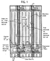
- Fig. 1 is a plan view showing one pixel and its periphery of the active matrix system color liquid crystal display device of the present invention.
- each pixel is disposed in an intersect region (region enclosed by four signal lines) defined by a gate line (scanning signal line or a horizontal signal line) GL, a counter line (counter voltage signal line) CL, neighboring two drain lines (image signal lines or vertical signal lines) DL.
- Each pixel includes a thin film transistor TFT, a storage capacitance C stg, a pixel electrode PX (called as a pixel electrode in this embodiment and means a display electrode) and a counter electrode CT (called as a counter electrode in this embodiment and means a reference electrode).
- the gate lines GL and the counter lines CL extend in a left and right direction in the drawing and are distributed in plural numbers in an upward and downward direction.
- the drain lines DL extend in a upward and downward direction in the drawing and are disposed in plural numbers in a left and right direction.
- the pixel electrodes PX are electrically connected to the thin film transistor TFT by way of source electrodes SD1 and the counter electrodes CT are also electrically connected to the counter lines CL.
- the pixel electrode PX and the counter electrode CT oppose to each other and an optical condition of a liquid crystal composition LC is controlled by an electric field approximately parallel to the surface of the substrate which is generated between each pixel electrode PX and the counter electrode CT and hence, the display is controlled.
- the pixel electrodes PX and the counter electrodes CT are constructed like a comb and are respectively formed of thin electrodes elongated in an upward and downward direction in the drawing.
- the electrode widths of the pixel electrodes PX and the counter electrodes CT are 6 ⁇ m respectively. This means that to apply a sufficient electric field on the entire liquid crystal layer against the direction of thickness of the liquid crystal layer, they are set to values sufficiently greater than 3. 9 ⁇ m which is the thickness of the liquid crystal composition layer which will be explained later. They may preferably be set 1. 5 times greater than the thickness of the liquid crystal composition layer. Furthermore, to increase the aperture efficiency, they are made as thin as possible. Furthermore, the drain lines DL are also set to 6 ⁇ m. To prevent the disconnection, the electrode width of the drain line DL may be slightly widened compared to the pixel electrodes PX and the counter electrodes CT.
- the width of the gate lines GL is set such that they meet the resistance value sufficient to propagate the scanning voltage to the gate electrode GT of the pixel at the tail end side (side opposite to gate electrode terminals GTM which will be explained later). Furthermore, the width of the counter line CL is set such that they meet the resistance value sufficient to apply a counter voltage to the counter electrode CT of the pixel at the tail end side (the pixel remotest from the common bus lines CB1, CB2 which will be explained later, namely, the pixel interposed between CB1 and CB2).
- the electrode interval between the pixel electrode PX and the counter electrode CT is varied depending on liquid crystal material used. This means that since the intensity of the electric field which achieves the miximum transmissivity depends on the liquid crystal material, the electrode interval is set depending on the liquid crystal material, and the electrode interval is set such that the maximum transmissivity is obtained in a range of the maximum amplitude of the signal voltage set corresponding to pressure resistance of the drain drive circuit (signal side driver) used. In case the liquid material which will be explained later is used, the interval between electrodes is approximately 15 ⁇ m.
- Fig. 2 is a view showing the cross section taken along a line 6 - 6 of Fig. 1
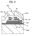
- Fig. 3 is a cross sectional view of the thin film transistor TFT taken along a line 7 - 7 of Fig. 1
- Fig. 4 is a view showing the cross section of the storage capacitance Cstg taken along a line 8 - 8 of Fig. 1.
- the thin film transistor TFT, the storage capacitance Cstg and a group of electrodes are formed at a lower portion transparent glass substrate SUB1 side, while a color filter FIL and a light blocking film (black matrix) BM are formed at an upper portion transparent glass substrate SUB2 side.
- orientation films OR11, OR12 which control the initial orientation of the liquid crystal are mounted and on respective surfaces of the outer sides (liquid crystal LC sides) of the transparent glass substrates SUB1, SUB2, polarizing plates are mounted.
- the thin film transistor TFT is operated such that when a positive bias is applied to the gate electrode GT, a channel resistance between the source and drain is reduced and when the bias becomes zero, the channel resistance is increased.
- the thin film transistor TFT includes the gate electrode GT, an insulating film GI, an i-type semiconductor layer AS made of an i-type (intrinsic or not doped with conductive type determination impurities) amorphous silicon (Si), a pair of source electrodes SD1, and the drain electrodes SD2.
- the source and drain are originally determined based on the bias polarity between them and such a polarity is inverted during operation in the circuit of this liquid crystal display device and hence, it should be understood that the source and drain are switched during operation. In the following explanation, however, for a convenience purpose, one is fixedly explained as the source, while the other is fixedly explained as the drain.
- the gate electrode GT is constructed such that it is formed contiguous with the gate line GL and a partial region of the gate line GL constitutes the gate electrode GT.
- the gate electrode GT is a portion which extends over an active region of the thin film transistor TFT.
- the gate electrode GT is made of a conductive film g3 having a single layer construction.
- a chrome-molybdenum alloy (Cr-Mo) film formed by spattering may be used as the conductive film g3, for example, the film is not limited to such material.
- the gate line GL is composed of the conductive film g3.
- the conductive film g3 of this gate line GL is formed in the same manufacturing step as the conductive film g3 of the gate electrode GT and is formed integrally with the conductive film g3 of the gate electrode GT.
- a gate voltage (a scanning voltage) Vg is supplied to the gate electrode GT from an external circuit.
- a chrome-molybdenum alloy (Cr-Mo) film formed by spattering may be used as the conductive film g3, for example.
- the gate line GL and the gate electrode GT are not limited to the chrome-molybdenum alloy and may have a two layer structure in which aluminum or aluminum alloy is wrapped by chrome-molybdenum for lowering the resistance. Still furthermore, a portion where the drain line DL and the gate line GL intersect is made narrow to minimize the probability of a short circuit with drain line DL. Alternately, the portion may be bifurcated so as to be cut out by a laser trimming even when the short-circuiting occurs.
- the counter line CL is composed of the conductive film g3.
- the conductive film g3 of this counter line CL is formed in the same step as the conductive films g3 of the gate electrode GT, the gate line GL and the counter electrode GT and is constructed to be electrically connected to the counter electrode CT.
- a counter voltage Vcom is supplied to the counter electrode CT from the outside.
- the counter line CL is not limited to the chrome-molybdenum alloy and may have a two layer structure in which aluminum or aluminum alloy is wrapped by chrome-molybdenum for lowering the resistance.
- a portion where the drain line DL and the counter line CL intersect is made narrow to minimize the probability of a short circuit with drain line DL. Alternately, the portion may be bifurcated so as to be cut out by a laser trimming even when the short-circuit occurs.
- the insulating film GI is used as a gate insulating film for applying an electric field to the semiconductor layer AS together with the gate electrode GT.
- the insulating film GI is formed on the gate electrode GT and the upper layer of the gate line GL.
- a silicon nitride film formed by a plasma CVD for example, can be chosen and the formed film has a thickness of 2000 - 4500 ⁇ (approximately 3500 ⁇ ).
- the insulating film GI also works as the interlayer insulating film among the gate line GL, the counter line CL and the drain line DL thus contributing to their electrical insulation.
- the i-type semiconductor layer AS is made of an amorphous silicon and is formed to a thickness of 150 - 2500 ⁇ (approximately 1200 ⁇ in this embodiment).
- a layer d0 is a N(+) type amorphous silicon semiconductor layer doped with phosphor (P) for an ohmic contact and is remained only at positions where the i-type semiconductor layer AS is present at a lower side thereof and the conductive layer d3 is present at an upper side thereof.
- the i-type semiconductor layers AS and the layer d0 are also provided between intersect portions (crossover portions) of the gate line GL and the counter line CL with the drain line DL.
- the i-type semiconductor layers AS reduces the short-circuiting of the gate line GL and the counter line CL with the drain line DL at these intersect portions.
- the source electrode SD1 and the drain electrode SD2 are respectively formed of conductive films d3 which are brought into contact with the N(+) type semiconductor layer d0.
- a chrome-molybdenum alloy (Cr-Mo) film formed by spattering is used as the conductive film d3 and the film is formed to a thickness of 500 - 3000 ⁇ (approximately 2500 ⁇ in this embodiment). Since the Co-Mo film has a low stress, it can be formed to have a relatively large thickness thus contributing to lowering of resistance of wires. Furthermore, the Co-Mo film exhibits a favorable adhesiveness to the N(+) type semiconductor layer d0.
- the conductive film d3 besides the Cr-Mo film, a high melting point metal (Mo, Ti, Ta, W) film or a high melting point metal suicide (MoSi2, TiSi2, TaSi2, WSi2) film can be used or the conductive film d3 may have a laminated structure with aluminum or the like.
- Mo, Ti, Ta, W high melting point metal
- MoSi2, TiSi2, TaSi2, WSi2 high melting point metal suicide
- the drain line DL is composed of a conductive layer d3 which is the same layer as the source electrode SD1 and the drain electrode SD2. Furthermore, the drain line DL is integrally formed with the drain electrode SD2.
- a chrome-molybdenum alloy (Cr-Mo) film formed by spattering is used as the conductive film d3 and the film is formed to a thickness of 500 - 3000 ⁇ (approximately 2500 ⁇ in this embodiment). Since the Cr-Mo film has a low stress, it can be formed to have a relatively large thickness thus contributing to lowering of resistance of wires. Furthermore, the Cr-Mo film exhibits a favorable adhesiveness to the N(+) type semiconductor layer d0.
- the conductive film d3 besides the Cr-Mo film, a high melting point metal (Mo, Ti, Ta, W) film or a high melting point metal silicide (MoSi2, TiSi2, TaSi2, WSi2) film can be used or the conductive film d3 may have a laminated structure with aluminum or the like for preventing the disconnection.
- Mo, Ti, Ta, W high melting point metal
- MoSi2, TiSi2, TaSi2, WSi2 high melting point metal silicide
- the conductive film d3 is formed such that it is overlapped or superposed onto the counter line CL at the source electrode SD2 of the thin film transistor TFT.
- this overlapping constitutes the storage capacitance (electrostatic capacitance element) C stg where the source electrode SD2-d3 defines one electrode and the counter line CL defines the other electrode.
- a dielectric film of this storage capacitance C stg is constituted by the insulating film GI which is used as a gate insulating film of the thin film transistor TFT.
- the storage capacitance Cstg is formed at a portion of counter line CL.
- the passivation layer PSV1 is mounted on the thin film transistor TFT.
- the passivation layer PSV1 is formed mainly for protecting the thin film transistor TFT from moisture or the like and the layer having a high transparency and a favorable moisture resistance is used.
- the passivation layer PSV1 is constituted by a silicon oxide film or a silicon nitride film formed by a plasma CVD apparatus and the formed layer has a thickness of approximately 0.05 - 0.3 ⁇ m. Since the main purpose of providing the passivation layer PSV1 is to protect a back channel portion of the thin film transistor element TFT, that is, to stabilize a threshold voltage Vth, in this embodiment, the passivation layer PSV1 is formed like an island only at the thin film transistor TFT portion. Due to such a construction, warping of the substrate caused by the stress of the passivation layer PSV1 can be reduced.
- the passivation layer PSV1 is removed such that external connection terminals DTM, GTM are exposed.
- the former is made thick in view of the protection effect and the latter is made thin in view of the mutual conductance gm of the transistor.
- the organic passivation layer PSV2 is mounted on the passivation layer PSV1.
- the organic passivation layer PSV2 is provided for the following purpose and the film having a high transparency and a low specific dielectric constant of approximately 3 can be used.
- the organic passivation layer PSV2 is made of, for example, a resist film formed by a coating apparatus and the film thickness is approximately 1 - 3 ⁇ m. Due to such a construction, the capacitance between the drain line and the counter electrode which is overlapped to the drain line can be drastically reduced. Accordingly, the load to the drain line is drastically reduced and the magnitude of a circuit of a drive LSI for driving the drain signal can be drastically minimized.
- the organic passivation layer PSV2 is useful in enhancing the flatness of the thin film transistor substrate. This is reasoned that the organic passivation layer can provide an improved flatness compared to the inorganic passivation layer.
- the organic passivation layer PSV2 is removed such that external connection terminals DTM, GTM are exposed. Furthermore, at the pixel portion, for assuring the electric connection between the counter line CL and the counter electrode CT which will be explained later and the electric connection between the source electrode SD2 and the pixel electrode PX, through holes TH2 and TH1 are formed. In the through hole TH2, the organic passivation layer PSV2 and the insulating film GI are worked simultaneouly so that the through hole TH2 reaches the g3 layer, while in the through hole TH1, it is blocked by the d3 so that the through hole TH1 reaches the d3 layer.
- the organic passivation layer having the specific dielectric constant of approximately 3 is used in this embodiment, the specific dielectric constant is preferably not greater than 4 to obtain the effect of the present invention.
- the pixel electrode PX is made of a transparent conductive layer i1 and is formed on the organic passivation layer PSV2.
- This transparent conductive film i1 is made of a transparent conductive film (Indium-Tin-Oxide ITO: nesa film) which is formed by spattering and the formed film has a thickness of 100 - 2000 ⁇ (approximately 1400 ⁇ in this embodiment).
- the pixel electrode PX is connected to the source electrode SD2 by way of the through hole TH1.
- the maximum dielectric constant at the time of making a white display is enhanced and hence, such pixel electrode can provide a brighter display than the opaque pixel electrode.
- liquid crystal molecules maintain the initial orientation condition, and since the polarizing plate is constructed such that the black display is made under such a condition (changed to a normally black mode), even when the pixel electrode is made transparent, no light is transmitted through the portion and hence, the high quality black can be displayed. Accordingly, the maximum dielectric constant can be enhanced and a sufficient contrast can be achieved.
- the counter electrode CT is made of a transparent conductive layer i1 and is formed on the organic passivation layer PSV2.
- This transparent conductive film i1 is made of a transparent conductive film (Indium-Tin-Oxide ITO: nesa film) which is formed by spattering and the formed film has a thickness of 100 - 2000 ⁇ (approximately 1400 ⁇ in this embodiment).
- the counter electrode CT is connected to the counter line CL by way of the through hole TH2.
- the pixel electrode PX by making the counter electrode transparent, the maximum transmissivity at the time of the white display can be enhanced.
- the drain line DL is completely covered by the counter electrode CT and most of the lines of electric force are terminated at the counter electrode CT. Due to such a construction, the leaked electric field from the drain line peculiar to the transverse electric field system can be completely eliminated thus completely dissolving the crosstalks. This is a special effect of the active matrix system liquid crystal display device using the transverse electric field system.
- the counter voltage V com is applied to the counter electrode CT.
- the counter voltage V com is set to a potential which is lower than an intermediate direct current potential between the minimum level drive voltage Vd min and the maximum level drive voltage Vd max applied to the drain line DL by a field through voltage ⁇ Vs generated when the thin film transistor element TFT is turned off.
- the light blocking film BM (a so-called black matrix) is formed so as prevent lowering of the contrast ratio which may be caused by emitting the transmitted light from unnecessary gap portions (gaps other than gaps between the pixel electrode PX and the counter electrode CT) onto the display surface side.
- the light blocking film BM also plays a role of preventing an outdoor daytime light and a back light from entering the i-type semiconductor layer AS. That is, the i-type semiconductor layer AS of the thin film transistor TFT is sandwiched by the light blocking film BM and the relatively larger gate electrode GT which are disposed above and below the layer thus preventing the outdoor natural light and the back light from being emitted to the layer.
- Fig. 1 shows one example of the pattern of the light blocking film BM.
- the pattern is of a matrix-like pattern forming apertures on the display portion of the pixel.
- the light blocking film BM is made of a chromium thin film.
- an chromium oxide or a chromium nitride is formed on the glass surface side of the chromium thin film. This is provided for reducing the reflectance thus making the display surface of the liquid crystal display device low-reflecting.
- respective effective display regions defined by respective lines and rows are partitioned by this light blocking film BM. Accordingly, the profile of the pixel of the respective row can be clarified by the light blocking film BM.
- the light blocking film BM is formed like a frame on the peripheral portion and its pattern is formed contiguously with the pattern of the matrix portion shown in Fig. 1.
- the light blocking film BM of the peripheral portion is extended outside of the seal portion SL thus preventing leaked light such as reflecting light or the like caused by apparatuses including personal computers on which the liquid crystal display device is mounted from entering the matrix portion and preventing the light such as the back light or the like from leaking to the outside of the display area.
- this light blocking film BM is held inwardly from the margin of the substrate SUB2 by approximately 0.3 - 1.0 mm and is formed while obviating the cut-out region of the substrate SUB2.
- an insulating light blocking film may be used provided that it has a sufficient light blocking effect.
- Color filters FIL are formed in stripes at positions opposed to the pixels, wherein the color filters appear repeatedly as red, green and blue. Color filters FIL are formed such that they are overlapped to edge portions of the light blocking film BM.
- the color filters FIL can be formed in the following manner. First of all, a dyeing base material such as acrylic based resin is formed on the surface of the upper transparent glass substrate SUB2. The dyeing base material other than the red filter forming region is removed by the photolithography technique. Thereafter, the dyeing base material is dyed by a red pigment and a fixing processing is applied so as to form the red filter R. Subsequently, applying the similar processes, a green filter G and a blue filter B are formed in sequence. A dyestuff may be used for dyeing.
- a dyeing base material such as acrylic based resin is formed on the surface of the upper transparent glass substrate SUB2.
- the dyeing base material other than the red filter forming region is removed by the photolithography technique. Thereafter, the dyeing base material is dyed by a red pigment and a fixing processing is applied so as to form the red filter R. Subsequently, applying the similar processes, a green filter G and a blue filter B are formed in sequence.
- a dyestuff
- the overcoat film OC is provided for preventing the leakage of the dyestuff of the color filter FIL to the liquid crystal composition layer LC and for flattening the step caused by the color filter FIL and the light blocking film BM.
- the overcoat film OC is formed of a transparent resin material such as acrylic resin or epoxy resin or the like. Furthermore, an organic passivation layer such as polyimide or the like having a favorable fluidity may be used as the overcoat film OC.
- liquid crystal material LC nematic liquid crystal with its anisotropy of dielectric constant ⁇ being positive and its value being 13.2 and its refractive index anisotropy ⁇ n being 0.081 (589 nm, 20°C ) is used.
- the liquid crystal layer has a thickness (gap) of 3.9 ⁇ m and a retardation ⁇ n.d of 0.316. With such a value of the retardation ⁇ n.d, when the orientation film which will be explained later and the polarizing plate are combined and the liquid crystal molecules are rotated from the rubbing direction to the electric field direction by 45°, the maximum dielectric constant can be obtained and hence, transmitting lights which have no wavelength dependency within a range of visible light can be obtained.
- the range of retardation is preferably in the range of 0.25 - 0.32 ⁇ m to obtain the sufficient transmission term.
- the thickness (gap) of the liquid crystal layer is controlled by polymer beads.
- the liquid crystal material LC is not specifically limited and its anisotropy of dielectric constant ⁇ may be negative. Furthermore, the greater the value of its anisotropy of dielectric constant ⁇ , the drive voltage can be reduced. Furthermore, the smaller its refractive index anisotropy ⁇ n, the thickness (gap) of the liquid crystal layer can be made thicker and hence, the liquid crystal fill-in time can be shortened and the irregularities of gap can be minimized.
- the specific resistance of the liquid crystal composition the value equal or more 10 9 ⁇ cm and not greater than 10 14 ⁇ cm or preferably the value equal or more 10 11 ⁇ cm and not greater than 10 13 ⁇ is used. According to this method, even when the resistance of the liquid crystal composition is low, the voltage applied between the pixel electrode and the counter electrode can be sufficiently held and its lower limit is 10 9 ⁇ cm and preferably 10 11 ⁇ cm. This is construed that the pixel electrode and the counter electrode are constructed on the same substrate. Furthermore, when the resistance is too high, it is difficult to alleviate static electricity which has entered in the manufacturing process and hence, the specific resistance should be not greater than 10 14 ⁇ cm and preferably not greater than 10 13 ⁇ cm.
- twist elastic constant K2 of the liquid crystal material should preferably be small, to be more specific, not less than 2pN.
- Polyimide is used as the orientation film ORI. Rubbing direction is parallel to each other between the upper and lower substrates and an angle which the orientation film OPI makes with an electric field applying direction is set to 75°.
- the angle which the rubbing direction and the electric field applying direction make is equal or more 45° and less than 90° when the anisotropy of dielectric constant ⁇ of the liquid crystal material is positive, while the angle is not less than 0° and greater than 45° when the anisotropy of dielectric constant ⁇ is negative.
- the polarizing plate POL As the polarizing plate POL, G1220DU manufactured by Nitto Denko Ltd. is used and the polarized light transmission axis MAX1 of the lower polarized plate POL1 is registered or aligned with the rubbing direction RDR, while the polarized light transmission axis MAX2 of the upper polarized plate POL2 is disposed perpendicular to the rubbing direction RDR. Due to such an arrangement, the normally closed characteristics in which corresponding to the increase of the voltage (voltage between the pixel electrode PX and the counter electrode CT) applied to the pixel of the present invention, the dielectric constant is increased can be obtained. Furthermore, when the voltage is not applied to the pixel, a high quality black display can be obtained. The relationship between the upper and lower polarized plates can be inverted and no substantial change takes place in characteristics by such an inversion.
- the conductivity is given to the polarized plates such that the polarized plates can cope with poor display or EMI caused by static electricity from the outside.
- the sheet resistance is preferably not greater than 10 8 ⁇ / ⁇ , while the polarized plates have to cope with EMI too, the sheet resistance is preferably not greater than 10 4 ⁇ / ⁇ .
- a conductive layer may be mounted on a rear surface (surface to which a polarized plate is adhered) opposite to the surface of the glass substrate for sandwiching the liquid crystal composition.
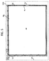
- Fig. 5 is a plan view showing the essential portions around the matrix (AR) of the display panel PNL including the upper and lower glass substrates SUB1, SUB2.
- Fig. 6 is a view showing the cross section in the vicinity of the external connection terminals GTM to which the scanning circuit is connected at its left side and the cross section in the vicinity of the sealed portion where no external connection terminals are provided at its right side.
- a glass substrate having a standardized size is processed and it is reduced to the size corresponding to the respective kind of panel.
- the glass is cut.
- Fig. 5 and Fig. 6 shows the latter example. Both Fig. 5 and Fig. 6 show the upper and lower substrates SUB1, SUB2 after cutting, wherein LN shows a margin of both substrates before cutting.
- the size of the upper substrate SUB2 is restricted such that it moves toward the inside than the lower substrate SUB1.
- the group of terminals Tg, Td are respectively named by assembling a plurality of scanning circuit connecting terminals GTM, image signal circuit connecting terminals DTM and drawing wiring portions which will be explained later for a unit of tape carrier package TCP (see Fig. 16, Fig. 17) on which integral circuit chips CHI mounted.
- the drawing wiring of each group extending from the matrix portion to the external connecting terminal portion are inclined as they approach both ends.
- This arrangement is provided for making the terminals DTM, GTM of the display panel PNL match the arranged pitch of the package TCP and the connecting terminal pitch at respective package TCP. Furthermore, counter electrode terminals COT are provided for applying a counter voltage to the counter electrodes CT from the external circuit .
- the counter lines CL of the matrix portion are drawn out to the side (right side in the drawing) opposite to the scanning circuit terminals GTM and respective counter lines are bundled at the common bus line CB and are connected to the counter electrodes COT.
- a seal pattern SL which seals the liquid crystal LC is formed except for a liquid crystal filling inlet INJ.
- the seal member may be made of epoxy resin, for example.
- Layers which constitute the orientation films OR11, OR12 are formed inside the seal pattern SL.
- the polarizing plates POL1, POL2 are respectively provided to the outside surfaces of the lower transparent glass substrate SUB1 and the upper transparent glass substrate SUB2.
- the liquid crystal LC is filled in a region partitioned by the seal pattern SL between the lower orientation film OR11 and the upper orientation film OR12 which determine the direction of the liquid crystal molecules.
- the lower orientation film OR11 is formed on the upper portion of the passivation layer PSV1 of the lower transparent glass substrate SUB1 side.
- This liquid crystal display device is assembled such that different kinds of layers are respectively stacked at the lower transparent glass substrate SUB1 side and the upper transparent glass substrate SUB2 side, the seal pattern SL is formed on the substrate SUB2 side, the lower transparent glass substrate SUB1 and the upper transparent glass substrate SUB2 are overlapped, the liquid crystal LC is filled into through the opening portion INJ of the seal member SL, the fill-in inlet INJ is closed by epoxy resin or the like, and the upper and the lower substrates are cut.
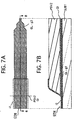
- Fig. 7 is a view showing a connection structure of the display matrix from the gate line GL to the external connecting terminals GTM, wherein Fig. 7A is a plan view and Fig. 7B is a cross-sectional view taken along a line B-B of Fig. 7A.
- Fig. 7A is a plan view
- Fig. 7B is a cross-sectional view taken along a line B-B of Fig. 7A.
- the gate terminal GTM is comprised of the Cr - Mo layer g3 and the transparent conductive layer i1 which protects the surface of the Cr - Mo layer g3 and enhances the reliability of its connection with the TCP (Tape Carrier Package).
- This transparent conductive layer i1 adopts the transparent conductive film ITO formed by the same step as that of the pixel electrode PX.
- an insulating film GI and the passivation layer PSV1 are formed at the right side from the border line, while the terminal portion GTM which is positioned at the left end side is exposed therefrom so as to be electrically brought into contact with an outer circuit.
- the gate line GL and the gate terminal are shown in the drawing, in an actual use, it is constructed such that these pairs are arranged in a plural numbers in an upward and downward direction thus constituting the group of terminals Tg (see Fig. 5) and, during the manufacturing process, the left ends of the gate terminals are extended over a cutting region of the substrates and are short-circuited by wiring SHg (not shown in drawings). They are useful for prevention of electrostatic breakdown at the time of rubbing of the orientation film OR11 during the manufacturing process.
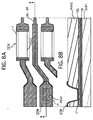
- Fig. 8 is a view showing the connection from the drain line DL to the external connection terminals DTM, wherein Fig. 8A is a plan view and Fig. 8B is a cross-sectional view taken along a line B-B of Fig. 8A.
- Fig. 8A is a plan view
- Fig. 8B is a cross-sectional view taken along a line B-B of Fig. 8A.
- These drawings correspond to a right upper portion and around the right upper portion of Fig. 5 and the right end direction corresponds to the upper end portion of the substrate SUB1 although the direction of the drawing is changed for a convenience purpose.
- TSTd indicates detection terminals.
- the external circuit is not connected here, the width thereof is widened than the wiring portion so as to make a probe needle to be brought into contact with the detection terminal.
- the width of the drain terminal DTM is also widened than the wiring portion so as to make the drain terminals DTM brought into contact with the external circuit.
- the external connection drain terminals DTM are arranged in an upward and downward direction.
- the drain terminals DTM as shown in Fig. 5, constitute a group of terminals Td (suffix being omitted) and they are extended over the cutting line of the substrate SUB1.
- the drain terminals DTM are all short-circuited by the wiring SHd not shown in the drawing so as to prevent the electrostatic breakdown during the manufacturing process.
- the detection terminals TSTd are formed into the drain lines DL which are arranged as every other one as shown in Fig. 8.
- the drain connection terminals DTM are made of transparent conductive layers i1 and portions thereof where the passivation layers PSV1 are removed are connected to the drain lines DL.
- This transparent conductive film i1 adopts the transparent conductive film ITO formed by the same process as that of the pixel electrode PX as is the case of gate terminals GTM.
- the draw-out line from the matrix portion to the drain terminal portion DTM is communicated by the layer d3 of the same level as the drain line DL.
- Fig. 9 is a view showing the connection from the counter line CL to the external connection terminals CTM, wherein Fig. 9A is a plan view and Fig. 9B is a cross-sectional view taken along a line B-B of Fig. 9A. These drawings correspond to a left upper portion and around the left upper portion of Fig. 5.
- Respective counter lines CL are bundled at the common bus line CB1 and are drawn out to the counter electrode terminals CTM.
- the common bus line CB is constructed such that the conductive layer 3 is laminated on the conductive layer g3 and they are electrically connected with each other by the transparent conductive layer i1. This is because that the resistance of the common bus line CB is reduced and hence, the counter voltage is sufficiently supplied to respective counter lines CL from the external circuit.
- This structure is characterized in that the resistance of the common bus can be reduced without providing any new conductive layer specifically.
- the counter electrode terminal CTM has a structure that the transparent conductive layer i1 is laminated on the conductive layer g3.
- This transparent conductive film i1 adopts the transparent conductive film ITO formed in the same step as the pixel electrode PX as is the case of other terminals.
- the counter electrode terminal CTM has the surface thereof covered by the transparent conductive layer i1 and the conductive layer g3 is covered with the transparent conductive layer i1 having a durability for preventing an electrolytic corrosion. Furthermore, the connection of the transparent conductive layer i1 with the conductive layer g3 and the conductive layer d3 is made by assuring a communication by forming through holes to the passivation layer PSV1 and the insulating film GI.
- Fig. 10 is a view showing the connection from another end of the counter line CL to the external connection terminals CTM2, wherein Fig. 10A is a plan view and Fig. 10B is a cross-sectional view taken along a line B-B of Fig. 10A.
- Fig. 10A is a plan view
- Fig. 10B is a cross-sectional view taken along a line B-B of Fig. 10A.
- respective counter lines CL have another ends thereof (gate terminal GTM side) bundled at the common bus line CB2 and are drawn out to the counter electrode terminals CTM2.
- the common bus line CB2 differs from the common bus line CB1 in that it is comprised of the conductive layer d3 and the transparent conductive layer i1 so as to be insulated from the gate line GL. Furthermore, the insulation against the gate line GL is assured by the insulating film GI.
- Fig. 11 The equivalent circuit of the display matrix portion and a wiring view of its peripheral circuit are shown in Fig. 11. Although the drawing is a circuit chart, it is described corresponding to an actual geometric arrangement.
- AR is a matrix array where a plurality of pixels are arranged in a two dimensional manner.
- X indicates a drain line DL
- suffixes G, B and R are added respectively corresponding to green, blue and red pixels.
- Y indicates a gate line GL and suffixes 1, 2, 3... , end are added in accordance with the sequence of a scanning timing.
- Gate lines Y (suffixed omitted) are connected to a gate driver V and drain lines X (suffix omitted) are connected to a drain driver H.
- SUP is a circuit which includes a power source circuit to obtain a plurality of partial-pressure stabilized voltage sources from one voltage source and a circuit which changes information for CRT (cathode ray tube) from a host (superior arithmetic unit) to information for TFT liquid crystal display device.
- a counter voltage Vch is set to a constant voltage.
- a scanning signal Vg takes an ON level at each scan period and takes an OFF level in the remaining period.
- An image signal voltage is applied such that it has an amplitude as twice as large as that of a voltage to be applied to the liquid crystal layer and its positive pole and negative pole are alternately inverted at each frame to transmit one pixel.
- the image signal voltage Vd has its polarity changed at each row and the polarity is also inverted at each line.
- the pixels are arranged such that the pixels which are neighboring to one pixel in upward and downward directions as well as in left and right directions have the inverted polarity and hence, flicker and crosstalk (smear in a left and right directions) hardly occur.
- the counter voltage Vc is set to a voltage which is a given amount lower than the center voltage with inverted polarity of the image signal voltage. This is performed so as to correct a field through voltage which is generated at the time that the thin film transistor element is changed over from ON to OFF and is also performed to apply an alternating current voltage having little direct component to the liquid crystal (since the liquid crystal often generates a residual image or a deterioration of image when the direct current is applied to the liquid crystal).
- the storage capacitance C stg is provided for storing image information written in the pixels for a long time (after the thin film transistor TFT is turned off).
- the storage capacitance C stg stores no image information in the pixel. Accordingly, in the system which applies the electric field parallel to the surface of the substrate, the storage capacitance C stg is an inevitable constructional element.
- ⁇ Vs ⁇ C gs /(C gs + C stg + C pix) ⁇ Vg
- C gs indicates a parasitic capacitance generated between the gate electrode GT and the source electrode SD1 of the thin film transistor TFT
- C pix indicates a capacitance generated between the pixel electrode PX and the counter electrode CT
- ⁇ Vs indicates an amount of change of the pixel electrode potential caused by ⁇ Vg, or a so-called feed through voltage.
- the gate electrode GT is made larger than the i-type semiconductor layer AS so as to completely cover the i-type semiconductor layer AS so that its overlapping area to the source electrode SD1 and the drain electrode SD2 is increased by an amount increased relative to the i-type semiconductor layer AS. Accordingly, the parasitic capacitance C gs is increased and an adverse effect that the pixel electrode potential Vs is liable to receive the influence of the gate (scanning) signal Vg. With the provision of the storage capacitance C stg, this demerit can be resolved.
- steps A - G are divided corresponding to the respective photographic treatment and respective cross-sectional views of respective steps show stages where the working after photographic treatment is finished and the photoresist is removed.
- the photographic treatment means a series of workings from applying of the photoresist to a developing by way of a selective exposure using a mask, and a repeated explanation is obviated. The method is hereinafter explained in view of divided steps.
- the conductive film g3 made of Cr-Mo or the like which has a film thickness of 2000 ⁇ is formed on the lower transparent glass substrate SUB1 made of AN635 glass (name of product) by spattering. After the photographic treatment, the conductive filme g3 is selectively etched using second cerium ammonium nitrate thus forming the gate electrodes GT, the gate lines GL, the counter lines CL, the gate terminals GTM, a first conductive layer of the common bus line CB1, first conductive layers of the counter electrode terminals CTM1 and the bus line SHg (not shown in drawings) which is connected with gate terminals GTM.
- Ammonia gas, silane gas, and nitrogen gas are introduced into the plasma CVD apparatus so as to form a silicon nitride film having a thickness of 3500 ⁇ , while silane gas and hydrogen gas are introduced into the plasma CVD apparatus so as to form the i-type amorphous Si film having a thickness of 1200 ⁇ , and ,thereafter, hydrogen gas and phosphine gas are introduced into the plasma CVD apparatus so as to form the N(+) type amorphous Si film having a thickness of 300 ⁇ .
- the N(+) type amorphous Si film or the i-type amorphous Si film is selectively etched by using SF6 or CC14 as a dry etching gas so as to form the island of the i-type semiconductor layer AS.
- the conductive film d3 made of Cr and having a thickness of 300 ⁇ is formed by spattering. After the photographic treatment, the conductive film d3 is etched using a liquid similar to that of the step A so as to form the drain line DL, the source electrode SD1, the drain electrode SD2, a first conductive layer of the common bus line CB2 and the bus line SHd (not shown in drawings) which makes the drain terminals DTM short-circuited. Subsequently, CC14, SF6 are introduced to a dry etching device so as to etch the N(+) type amorphous Si film thus selectively removing an N(+) type semiconductor layer d0 disposed between the source and the drain.
- the N(+)type semiconductor layer d0 is excepted by the mask of conductive film d3. That is, the N(+) type semiconductor layer d0 remaining on the i-type semiconductor layer AS is removed by a self aligning except for the conductive layer d1 and the conductive layer d2. In such a case, the N(+) type semiconductor layer d0 is totally removed to its thickness by etching so that the i-type semiconductor layer AS is slightly removed by etching. However, the degree of such an etching can be controlled by means of the etching time.
- Ammonia gas, silane gas, and nitrogen gas are introduced into the plasma CVD apparatus so as to form a silicon nitride Si film having a thickness of 0.3 ⁇ m.
- a patterning of the passivation layer PSV1 is performed.
- the insulating film GI is subjected to the dry etching in the same manner as that of the step E. Accordingly, the organic passivation layer PSV2 and the insulating film GI are collectively subjected to working including the patterning while using the same photomask.
- the transparent conductive film i1 which is made of an ITO film and has a film thickness of 1400 ⁇ is formed by spattering. After the photographic treatment, the transparent conductive film i1 is selectively etched using a mixed acid liquid made of hydrochloric acid and nitric acid as an etchant so as to form an uppermost layer of the gate terminals GTM, the drain terminals DTM and counter electrode terminals CTM1 and a second conductive layer of CTM2.
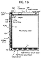
- Fig. 16 shows a top plan view showing a condition where the drain driver H and the gate driver V are connected to the display panel PNL shown in Fig. 5 and the like.
- CHI indicates drive IC chips for driving the display panel PNL (lower-side 5 pieces are drive IC chips of the gate driver side and left-side 10 pieces are drive IC chips of the drain driver side).
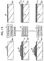
- TCP is a tape carrier package on which drive IC chips CHI are mounted as explained later in view of Fig. 13 and Fig. 14 by a tape automated bonding method (TAB), while PCB1 is a drive circuit board on which the above-mentioned TCP and capacitors and the like are mounted and is divided in two for the drain driver and for the gate driver.
- FGP indicates a frame grand pad and is produced by soldering spring shaped pieces which are formed by cutting in a shield case SHD.
- FC indicates a flat cable for electrically connecting the lower-side drive circuit board PCB1 with the left-side drive circuit board PCB1.
- a flat cable FC as shown in the drawings, the cable which sandwiches and supports a plurality of lead wires (Sn plated to phosphor bronze as raw material) by means of polyethylene layer and polyvinylalcohol layer in stripes is used.
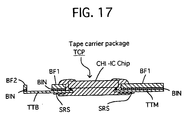
- Fig. 17 shows the cross-sectional structure of the tape carrier package TCP which constitutes the gate driver V and the drain driver H and in which integrated circuit chips CHI are mounted on a flexible wiring board.
- Fig. 18 is a cross-sectional view of an essential portion where the tape carrier package TCP is connected to the scanning signal circuit terminals GTM of the liquid crystal display panel in this example.
- TTB indicates an input terminal and wiring portion of the integrated circuit CHI
- TTM indicates an output terminal and wiring portion.
- They are made of Cu, for example, and bonding pads PAD of the integrated circuits CHI are respectively connected to the inner distal ends (usually called as inner leads) thereof by a face-down bonding method.
- Outside distal end portions (usually called as outer leads) of the terminals TTB, TTM respectively correspond to the inputs and the outputs of the semiconductor integrated circuit chips CHI and are connected to a CRT/TFT converting circuit/power source circuit SUP by solder bonding or the like and are connected to the liquid crystal display panel PNL by means of an anisotropic conductive film ACF.
- a package TCP is connected to the panel such that the distal end thereof covers the passivation layer PSV1 which has the panel PNL-side connecting terminals GTM exposed. Accordingly, the external connecting terminals GTM (DTM) are covered by at least either one of the passivation layer PSV1 or the package TCP and hence, it has a sufficient resistance against an electrolytic corrosion.
- BF1 is a base film made of polyimide or the like and SRS is a solder resist film for masking to prevent the solder from adhering to unnecessary portions during soldering.
- the gap defined between the upper and lower glass substrates at the outside of the seal pattern SL is protected by epoxy resin EPX or the like after being cleaned and furthermore, silicone resin SIL is charged between the package TCP and the upper substrate SUB2 so as to provide a multiplied protection.
- the drive circuit board PCB2 On the drive circuit board PCB2, electronic components such as ICs, capacitors and resistors and the like are mounted. On this drive circuit board PCB2, a power source circuit for obtaining a plurality of partial-pressure stabilized voltage sources, and the circuit SUP including a circuit for converting information for CRT (cathode ray tube) supplied from a host (superior arithmetic unit) into information for TFT liquid crystal display device are mounted.
- CJ is a connector connecting portion to which a connector not shown in the drawing is connected with the outside is connected.
- the drive circuit board PCB1 and the drive circuit board PCB2 are electrically connected with each other by means of the flat cable FC.
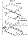
- Fig. 19 is an exploded perspective view of respective components of the liquid crystal display module MDL.
- SHD indicates a frame-like shield case (metal frame) made of a metal plate
- LCW indicates a display window
- PNL indicates a liquid crystal display panel
- SPB indicates a light diffusion plate
- LCB indicates a light guide body
- RM indicates a reflecting plate
- BL indicates a back light fluorescent tube
- LCA is a back light case.
- Respective members are stacked while keeping the vertical arrangement relationship shown in the drawing to assemble the module MDL.
- the module MDL has its entire body fixedly secured by means of pawls and hooks mounted on the shield case SHD.
- the back light case LCA has a shape suitable for accommodating the back light lamp BL, the light diffusion plate SPB, the light guide body LCB and the reflection plate RM.
- Light of the back light lamp BL which is disposed on the side surface of the light guide body LCB is turned into a back light which is uniform on the display surface by means of the light guide body LCB, the reflection plate RM and the light diffusion plate SPB and is emitted to the liquid crystal display panel PNL side.
- An inverter circuit board PC3 is connected to the back light lamp BL and this constitutes the power source of the back light lamp BL.
- the effect of the liquid crystal display element constructed in the above manner is generated by following three operations.
- the reference electrode Against the drain line formed on one transparent substrate side, the reference electrode is formed on the organic insulating film in a completely overlapped condition in a plan view and hence, almost whole lines of unnecessary lines of electric force generated from the drain line are terminated at the reference electrode. Accordingly, crosstalk caused by the leaked electric field peculiar to the display system such as the system of the present invention which adopts the transverse electric field can be eliminated. Therefore, the leaked electric field can be more completely shielded than the shield electrodes which have been conventionally disposed at both sides of the drain line or on the counter substrate for reducing the crosstalk and hence, the horizontal direction of the pixels can be occupied by the display electrode, the reference electrode and the opening.
- the specific dielectric constant of the organic insulating film is approximately half (the specific dielectric constant ⁇ r being about 3) of the inorganic insulating film. Furthermore, since the organic passivation layer can easily increase its thickness compared to the inorganic passivation layer, the distance between the drain line and the reference electrode is widened. Even when the drain line is completely overlapped by the reference electrode, the capacitance generated between the drain line and the reference electrode can be considerably made small. Accordingly, the load as seen from the drain line becomes small so that wiring propagation delay of the image signal becomes small, the signal voltage is sufficiently charged to the display electrode, and the drive circuit for driving the drain line can be minimized.
- the organic passivation layer has an excellent flatness so that by coating the organic passivation layer onto the top layer of the substrate which constitutes an active element, the flatness of the substrate which constitutes the active element is enhanced. Accordingly, irregularities of brightness (transmissivity) - voltage characteristics which is caused by the irregularities of gap between the substrates can be eliminated and hence, the uniformity of the brightness can be enhanced.
- the so-called longitudinal smear which is a fundamental problem to the liquid crystal display device of an extremely broad angle of visual field which adopts the transverse electric field system can be restricted. Accordingly, the reduction of the power consumption and the size reduction of the peripheral circuit are simultaneously achieved. Furthermore, the uniformity of the brightness can be enhanced.
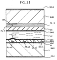
- Fig. 20 is a plan view of the pixel and Fig. 21 is a cross-sectional view of a comb-shaped electrode portion.
- the pixel electrode PX is comprised of a source electrode SD1, a drain electrode SD2 and a conductive film d3 on the same layer as the drain electrode SD2. Furthermore, the pixel electrode PX is integrally formed with the source electrode SD1.
- a contact failure with the pixel electrode PX can be avoided although the transmissivity is sacrificed. Furthermore, since the pixel electrode PX is covered with the insulating film (the passivation layer PSV1), when there exists an orientation failure, the possibility that the direct current flows through the liquid crystal is lowered thus eliminating the deterioration and the like of the liquid crystal and the reliability is further enhanced compared to the embodiment 1.
- Fig. 22 is a cross-sectional view of the pixel of this embodiment.
- the passivation layer PSV1 and the organic passivation layer PSV2 are collectively removed such that the external connecting terminals DTM, GTM are exposed. Accordingly, different from the embodiment 1, the passivation layer PSV1 is formed on most of the pixel. Furthermore, in the pixel portion, for assuring an electric connection between the counter line CL and the counter electrode CT which will be explained later and an electric connection between the source electrode SD2 and the pixel electrode PX, through holes TH2 and TH1 are formed.
- the organic passivation layer PSV2, the passivation layer PSV1 and the insulating film GI are collectively subjected to working and a hole which reaches the layer g3 is formed, while at the through hole TH1, the organic passivation layer PSV2 and the passivation layer PSV1 are collectively subjected to working and a hole is blocked by the layer d3 thus forming the hole which reaches the layer d3.
- resist material is used for the organic passivation layer PSV2.
- the resist material is developed by photolithography, the resist material at the through hole portion is removed, and the pattern of the resist material is formed.
- the passivation layer PSV1 and the insulating film G1 are collectively etched to form the pattern of the passivation layer PSV1 and the insulating film GI.
- This step is as same as the step for forming TFT of the embodiment 1.
- this resist material is removed usually, in this embodiment, the resist material is remained and is used as the organic passivation layer PSV2.
- the passivation layer PSV1 by setting the thickness of the passivation layer PSV1 to 0.1 ⁇ m which is an extremely thin value, an etching time of the passivation layer PSV1 is prevented from being prolonged and hence, the throughput is enhanced.
- the passivation layer PSV1 is provided for protecting the back channel portion of the thin film transistor element TFT, that is, for stabilizing the threshold voltage Vth of the thin film transistor and it is sufficient if the thickness of 0.05 to 0.3 ⁇ m is assured.
- the passivation layer PSV1, the organic passivation layer PSV2 and the insulating film GI are respectively and independently produced through individual photolithography step using indivisual photo masks, in this embodiment, they can be performed collectively using a single mask and hence, the throughput for producing the TFT substrate is greatly enhanced compared to the first embodiment and as a result, the mass productivity is greatly enhanced.
- the collective working of the organic passivation layer PSV2 and the insulating film GI and the collective working of the organic passivation layer PSV2 and the passivation layer PSV1 can be performed in the same manner as this embodiment and they belong to the category or scope of the present invention.
- This embodiment is similar to the embodiment 1 except for the following.
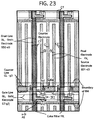
- Fig. 23 is a plan view showing one pixel and its periphery of the active matrix system color liquid crystal display device of this embodiment.
- the light blocking films BM in stripes are formed only in a horizontal direction of the pixel pattern.
- this embodiment it is sufficient to perform only a shielding of light on the TFT and a shielding of light at the light leaking portion between the counter electrode and the gate line.
- this embodiment can greatly enhance the aperture efficiency and hence, this embodiment can enhance the brightness in addition to the effects of the embodiment 1.
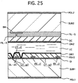
- Fig. 24 is a plan view of the pixel and Fig. 25 is a cross-sectional view of the comb electrode portion.
- the counter electrode CT includes a portion which protrudes from the gate line GL, the gate electrode GT and the counter line CL which is constructed by the conductive film g3 on the same layer as the counter line CL and a portion which is formed of the conductive film i1 on the passivation layer PSV2 as in the case of the embodiment 2. Furthermore, through holes are formed in the portion protruding from the counter line CL made of the conductive film g3 and the portion formed of the conductive film i1 on the passivation layer PSV2 and they are electrically connected with each other and are constructed such that they embrace the drain line.
- this embodiment can reduce the leaked electric field peculiar to the transverse electric field system more effectively than the embodiment 1 and the embodiment 2 so that crosstalk can be resolved.
- liquid crystal display device of the present invention a so-called longitudinal smear which is an intrinsic problem in the liquid crystal display device having a super broad visual field angle and adopting the transverse electric field system can be restricted thus enabling the enhancement the brightness, the reduction of the power consumption, the downsizing of the peripheral circuit and the enhancement of the uniformity of the brightness.
Landscapes
- Physics & Mathematics (AREA)
- Nonlinear Science (AREA)
- Engineering & Computer Science (AREA)
- Mathematical Physics (AREA)
- Chemical & Material Sciences (AREA)
- Crystallography & Structural Chemistry (AREA)
- General Physics & Mathematics (AREA)
- Optics & Photonics (AREA)
- Microelectronics & Electronic Packaging (AREA)
- Manufacturing & Machinery (AREA)
- Geometry (AREA)
- Liquid Crystal (AREA)
Applications Claiming Priority (3)
| Application Number | Priority Date | Filing Date | Title |
|---|---|---|---|
| JP9344097 | 1997-04-11 | ||
| JP9344097 | 1997-04-11 | ||
| PCT/JP1998/001500 WO1998047044A1 (fr) | 1997-04-11 | 1998-04-01 | Dispositif d'affichage a cristaux liquides |
Publications (3)
| Publication Number | Publication Date |
|---|---|
| EP1008896A1 true EP1008896A1 (fr) | 2000-06-14 |
| EP1008896A4 EP1008896A4 (fr) | 2005-05-18 |
| EP1008896B1 EP1008896B1 (fr) | 2006-09-13 |
Family
ID=14082395
Family Applications (1)
| Application Number | Title | Priority Date | Filing Date |
|---|---|---|---|
| EP98911154A Expired - Lifetime EP1008896B1 (fr) | 1997-04-11 | 1998-04-01 | Dispositif d'affichage a cristaux liquides |
Country Status (7)
| Country | Link |
|---|---|
| US (10) | US6208399B1 (fr) |
| EP (1) | EP1008896B1 (fr) |
| JP (1) | JP3674953B2 (fr) |
| KR (2) | KR100697903B1 (fr) |
| DE (1) | DE69835888T2 (fr) |
| TW (1) | TW531686B (fr) |
| WO (1) | WO1998047044A1 (fr) |
Cited By (6)
| Publication number | Priority date | Publication date | Assignee | Title |
|---|---|---|---|---|
| WO2003069401A1 (fr) | 2002-02-13 | 2003-08-21 | Koninklijke Philips Electronics N.V. | Dispositif d'affichage a cristaux liquides |
| CN100345053C (zh) * | 2003-11-04 | 2007-10-24 | Lg.菲利浦Lcd株式会社 | 利用水平电场的薄膜晶体管基板及其制造方法 |
| US7362401B2 (en) | 1997-10-16 | 2008-04-22 | Mitsubishi Denki Kabushiki Kaisha | In plane switching liquid crystal displaying apparatus for improved luminance including a thin film transistor array substrate |
| EP2076104A2 (fr) * | 2007-12-27 | 2009-07-01 | LG Electronics Inc. | Film flexible et dispositif d'affichage comportant ce film |
| CN102566168A (zh) * | 2010-12-30 | 2012-07-11 | 上海天马微电子有限公司 | 阵列基板及其制作方法、液晶显示装置 |
| US8808837B2 (en) | 2007-12-21 | 2014-08-19 | Lg Electronics Inc. | Flexible film and display device comprising the same |
Families Citing this family (133)
| Publication number | Priority date | Publication date | Assignee | Title |
|---|---|---|---|---|
| US6532053B2 (en) * | 1996-12-18 | 2003-03-11 | Hitachi, Ltd. | Transverse electric field system liquid crystal display device suitable for improving aperture ratio |
| US6972818B1 (en) * | 1997-05-19 | 2005-12-06 | Lg.Philips Lcd Co., Ltd. | In-plane switching mode liquid crystal display device |
| JPH11174491A (ja) * | 1997-12-08 | 1999-07-02 | Nec Corp | アクティブマトリクス型液晶表示装置 |
| US20040109103A1 (en) * | 1998-06-30 | 2004-06-10 | Hitachi, Ltd. | Liquid crystal display device |
| US6287899B1 (en) * | 1998-12-31 | 2001-09-11 | Samsung Electronics Co., Ltd. | Thin film transistor array panels for a liquid crystal display and a method for manufacturing the same |
| JP2000199915A (ja) * | 1999-01-06 | 2000-07-18 | Matsushita Electric Ind Co Ltd | 液晶表示パネル |
| US7202924B1 (en) * | 1999-03-17 | 2007-04-10 | Lg.Philips Lcd Co., Ltd | Liquid crystal display and a fabricating method thereof |
| JP2000275666A (ja) * | 1999-03-25 | 2000-10-06 | Hitachi Ltd | 液晶表示装置 |
| US6630977B1 (en) * | 1999-05-20 | 2003-10-07 | Semiconductor Energy Laboratory Co., Ltd. | Semiconductor device with capacitor formed around contact hole |
| JP3576871B2 (ja) * | 1999-06-04 | 2004-10-13 | 日本電気株式会社 | アクティブマトリクス型液晶表示装置 |
| US6762816B1 (en) * | 1999-06-11 | 2004-07-13 | Matsushita Electric Industrial Co., Ltd. | Liquid crystal display with special electrode configurations and compositions and method for producing the same |
| JP4724339B2 (ja) | 1999-09-07 | 2011-07-13 | 株式会社日立製作所 | 液晶表示装置 |
| JP3391343B2 (ja) * | 1999-10-26 | 2003-03-31 | 日本電気株式会社 | アクティブマトリクス基板及びその製造方法 |
| KR100595294B1 (ko) * | 1999-12-14 | 2006-07-03 | 엘지.필립스 엘시디 주식회사 | 횡전계방식 액정표시장치용 칼라필터 기판의 제조방법 |
| JP2001343667A (ja) * | 2000-03-29 | 2001-12-14 | Sharp Corp | 表示装置およびその欠陥修正方法 |
| KR100859232B1 (ko) * | 2000-04-05 | 2008-09-18 | 마쯔시다덴기산교 가부시키가이샤 | 액정표시패널 |
| KR100736114B1 (ko) * | 2000-05-23 | 2007-07-06 | 엘지.필립스 엘시디 주식회사 | 횡전계 방식의 액정표시장치 및 그 제조방법 |
| JP3564417B2 (ja) * | 2000-05-31 | 2004-09-08 | Nec液晶テクノロジー株式会社 | カラー液晶表示装置及びその製造方法 |
| JP3723747B2 (ja) * | 2000-06-16 | 2005-12-07 | 松下電器産業株式会社 | 表示装置およびその駆動方法 |
| JP3427981B2 (ja) * | 2000-07-05 | 2003-07-22 | 日本電気株式会社 | 液晶表示装置及びその製造方法 |
| JP2002139737A (ja) * | 2000-07-31 | 2002-05-17 | Matsushita Electric Ind Co Ltd | 液晶表示装置とその製造方法 |
| JP2002062544A (ja) * | 2000-08-22 | 2002-02-28 | Nec Corp | アクティブマトリクス型液晶表示装置 |
| KR100469341B1 (ko) * | 2000-08-30 | 2005-01-31 | 엘지.필립스 엘시디 주식회사 | 횡전계방식 액정표시장치 및 그 제조방법 |
| JP2002090778A (ja) * | 2000-09-20 | 2002-03-27 | Hitachi Ltd | 液晶表示装置 |
| TWI284240B (en) * | 2000-09-27 | 2007-07-21 | Matsushita Electric Industrial Co Ltd | Liquid crystal display device |
| JP2002148659A (ja) | 2000-11-10 | 2002-05-22 | Hitachi Ltd | 液晶表示装置 |
| JP2002162415A (ja) * | 2000-11-28 | 2002-06-07 | Japan Electronic Materials Corp | プローブカード用プローブ |
| JP4667587B2 (ja) * | 2000-12-01 | 2011-04-13 | 株式会社日立製作所 | 液晶表示装置 |
| JP2002182243A (ja) * | 2000-12-15 | 2002-06-26 | Nec Corp | 液晶表示装置用トランジスタ基板及びその製造方法 |
| JP4884586B2 (ja) * | 2000-12-18 | 2012-02-29 | 株式会社 日立ディスプレイズ | 液晶表示装置 |
| JP3949897B2 (ja) * | 2001-01-29 | 2007-07-25 | 株式会社日立製作所 | 液晶表示装置 |
| JP4603560B2 (ja) * | 2001-02-23 | 2010-12-22 | Nec液晶テクノロジー株式会社 | 横電界方式のアクティブマトリクス型液晶表示装置及び電子機器 |
| JP2002323706A (ja) * | 2001-02-23 | 2002-11-08 | Nec Corp | 横電界方式のアクティブマトリクス型液晶表示装置及びその製造方法 |
| JP5046064B2 (ja) * | 2001-02-23 | 2012-10-10 | Nltテクノロジー株式会社 | 横電界方式のアクティブマトリクス型液晶表示装置 |
| US7095460B2 (en) * | 2001-02-26 | 2006-08-22 | Samsung Electronics Co., Ltd. | Thin film transistor array substrate using low dielectric insulating layer and method of fabricating the same |
| JP5165169B2 (ja) * | 2001-03-07 | 2013-03-21 | 株式会社ジャパンディスプレイイースト | 液晶表示装置 |
| JP2002268084A (ja) * | 2001-03-08 | 2002-09-18 | Sharp Corp | アクティブマトリクス基板及びその製造方法 |
| JP4831716B2 (ja) * | 2001-03-15 | 2011-12-07 | Nltテクノロジー株式会社 | アクティブマトリクス型液晶表示装置 |
| JP4718712B2 (ja) * | 2001-04-17 | 2011-07-06 | Nec液晶テクノロジー株式会社 | アクティブマトリクス型液晶表示装置 |
| JP4943589B2 (ja) * | 2001-04-26 | 2012-05-30 | ゲットナー・ファンデーション・エルエルシー | 液晶表示装置の製造方法 |
| KR100803177B1 (ko) * | 2001-05-14 | 2008-02-14 | 삼성전자주식회사 | 액정표시장치용 박막 트랜지스터 및 그 제조방법 |
| KR100744955B1 (ko) * | 2001-05-21 | 2007-08-02 | 엘지.필립스 엘시디 주식회사 | 횡전계방식 액정표시장치용 어레이기판과 그 제조방법 |
| JP3946547B2 (ja) * | 2001-06-05 | 2007-07-18 | シャープ株式会社 | アクティブマトリクス基板および表示装置ならびに検出装置 |
| JP4876341B2 (ja) * | 2001-07-13 | 2012-02-15 | 日本電気株式会社 | アクティブマトリクス基板及びその製造方法 |
| TWI298110B (en) * | 2001-07-31 | 2008-06-21 | Hitachi Ltd | Liquid crystal display device |
| JP5038560B2 (ja) * | 2001-08-01 | 2012-10-03 | ゲットナー・ファンデーション・エルエルシー | 電界効果型トランジスタ及びその製造方法並びに該トランジスタを使った液晶表示装置及びその製造方法 |
| JP2003140188A (ja) * | 2001-11-07 | 2003-05-14 | Hitachi Ltd | 液晶表示装置 |
| JP2003149674A (ja) * | 2001-11-13 | 2003-05-21 | Hitachi Ltd | 液晶表示装置 |
| KR100752213B1 (ko) * | 2001-12-20 | 2007-08-28 | 엘지.필립스 엘시디 주식회사 | 액정표시소자 |
| KR100652063B1 (ko) * | 2001-12-27 | 2006-11-30 | 엘지.필립스 엘시디 주식회사 | 액정표시소자 및 그 제조방법 |
| JP4162890B2 (ja) * | 2001-12-27 | 2008-10-08 | 株式会社日立製作所 | 液晶表示装置 |
| KR100473588B1 (ko) * | 2001-12-28 | 2005-03-08 | 엘지.필립스 엘시디 주식회사 | 액정 표시 장치용 어레이 기판 |
| KR100801153B1 (ko) * | 2001-12-31 | 2008-02-05 | 엘지.필립스 엘시디 주식회사 | 횡전계방식 액정표시장치용 어레이기판과 그 제조방법 |
| JP3891846B2 (ja) * | 2002-01-15 | 2007-03-14 | 株式会社日立製作所 | 液晶表示装置 |
| JP3586674B2 (ja) * | 2002-01-30 | 2004-11-10 | Nec液晶テクノロジー株式会社 | 液晶表示装置 |
| JP3957277B2 (ja) * | 2002-04-15 | 2007-08-15 | 株式会社アドバンスト・ディスプレイ | 液晶表示装置及びその製造方法 |
| US6833897B2 (en) * | 2002-04-19 | 2004-12-21 | Hannstar Display Corp. | IPS-LCD device with a color filter formed on an array substrate |
| JP4085170B2 (ja) * | 2002-06-06 | 2008-05-14 | 株式会社 日立ディスプレイズ | 液晶表示装置 |
| JP2004077718A (ja) * | 2002-08-15 | 2004-03-11 | Hitachi Displays Ltd | 液晶表示装置 |
| US6970223B2 (en) * | 2002-08-17 | 2005-11-29 | Lg. Philips Lcd Co., Ltd. | In-plane switching mode LCD device and method for fabricating the same |
| JP4199501B2 (ja) | 2002-09-13 | 2008-12-17 | Nec液晶テクノロジー株式会社 | 液晶表示装置の製造方法 |
| JP2004109794A (ja) * | 2002-09-20 | 2004-04-08 | Hitachi Displays Ltd | 液晶表示装置 |
| JP4248848B2 (ja) * | 2002-11-12 | 2009-04-02 | 奇美電子股▲ふん▼有限公司 | 液晶表示セルおよび液晶ディスプレイ |
| KR100917324B1 (ko) * | 2002-11-16 | 2009-09-11 | 엘지디스플레이 주식회사 | 모바일 폰용 액정표시장치 |
| US7046315B2 (en) * | 2002-12-06 | 2006-05-16 | Lg.Philips Lcd Co., Ltd. | Array substrate of liquid crystal display device having color filter on thin film transistor structure and method of fabricating the same |
| JP4194362B2 (ja) * | 2002-12-19 | 2008-12-10 | 奇美電子股▲ふん▼有限公司 | 液晶表示セルおよび液晶ディスプレイ |
| JP4176487B2 (ja) * | 2003-01-15 | 2008-11-05 | 株式会社 日立ディスプレイズ | 液晶表示装置 |
| JP4720970B2 (ja) * | 2003-03-19 | 2011-07-13 | 日本電気株式会社 | 液晶表示装置 |
| US7494596B2 (en) * | 2003-03-21 | 2009-02-24 | Hewlett-Packard Development Company, L.P. | Measurement of etching |
| JP4505192B2 (ja) * | 2003-03-31 | 2010-07-21 | シャープ株式会社 | 液晶パネルの製造方法 |
| KR100560401B1 (ko) * | 2003-11-04 | 2006-03-14 | 엘지.필립스 엘시디 주식회사 | 수평 전계 인가형 박막 트랜지스터 기판 및 그 제조 방법 |
| KR100538328B1 (ko) * | 2003-06-20 | 2005-12-22 | 엘지.필립스 엘시디 주식회사 | 액정표시장치 및 그 제조방법 |
| KR100741890B1 (ko) * | 2003-06-26 | 2007-07-23 | 엘지.필립스 엘시디 주식회사 | 횡전계 방식의 액정표시장치 및 그의 제조방법 |
| KR100675631B1 (ko) * | 2003-06-27 | 2007-02-01 | 엘지.필립스 엘시디 주식회사 | 횡전계방식 액정표시장치 및 그 제조방법 |
| KR100560404B1 (ko) * | 2003-11-04 | 2006-03-14 | 엘지.필립스 엘시디 주식회사 | 수평 전계 인가형 박막 트랜지스터 기판 및 그 제조 방법 |
| US7202523B2 (en) * | 2003-11-17 | 2007-04-10 | Micron Technology, Inc. | NROM flash memory devices on ultrathin silicon |
| KR100698059B1 (ko) * | 2003-12-27 | 2007-03-23 | 엘지.필립스 엘시디 주식회사 | 액정표시장치 및 이의 제조방법 |
| KR101186863B1 (ko) * | 2003-12-29 | 2012-10-05 | 엘지디스플레이 주식회사 | 멀티도메인 횡전계모드 액정표시소자 |
| JP4462981B2 (ja) | 2004-03-29 | 2010-05-12 | Nec液晶テクノロジー株式会社 | アクティブマトリクス基板及び該基板を備える液晶表示装置 |
| CN101057174A (zh) * | 2004-04-13 | 2007-10-17 | 庄臣及庄臣视力保护公司 | 用于电活性液晶眼科设备的图案化电极 |
| JP4554983B2 (ja) * | 2004-05-11 | 2010-09-29 | Nec液晶テクノロジー株式会社 | 液晶表示装置 |
| JP4846301B2 (ja) * | 2004-08-30 | 2011-12-28 | サムスン エレクトロニクス カンパニー リミテッド | 薄膜トランジスタ基板の製造方法及びストリッピング組成物 |
| KR100652061B1 (ko) | 2004-11-04 | 2006-12-06 | 엘지.필립스 엘시디 주식회사 | 컬러필터 기판 및 그 제조방법, 및 그를 이용한액정표시소자 및 그 제조방법 |
| JP2006178235A (ja) * | 2004-12-22 | 2006-07-06 | Nec Corp | 薄膜トランジスタアレイ基板及び液晶表示装置 |
| KR101133758B1 (ko) * | 2005-01-19 | 2012-04-09 | 삼성전자주식회사 | 센서 및 이를 구비한 박막 트랜지스터 표시판 |
| KR101133764B1 (ko) * | 2005-03-14 | 2012-04-09 | 삼성전자주식회사 | 박막 트랜지스터, 박막 트랜지스터 표시판 및 그 제조 방법 |
| US7486336B2 (en) * | 2005-03-31 | 2009-02-03 | Mstar Semiconductor, Inc. | ADC system, video decoder and related method for decoding composite video signal utilizing clock synchronized to subcarrier of composite video signal |
| KR20060121370A (ko) * | 2005-05-24 | 2006-11-29 | 삼성전자주식회사 | 액정표시장치의 제조방법과 이에 의한 액정표시장치 |
| US7443477B2 (en) * | 2005-09-06 | 2008-10-28 | Hannstar Display Corporation | In-plane switching liquid crystal display |
| KR20070080050A (ko) * | 2006-02-06 | 2007-08-09 | 삼성전자주식회사 | 액정 표시 장치 및 그 제조 방법 |
| TW200730978A (en) * | 2006-02-08 | 2007-08-16 | Wintek Corp | Active matrix liquid crystal display and pixel structure thereof |
| JP4622917B2 (ja) * | 2006-03-30 | 2011-02-02 | エプソンイメージングデバイス株式会社 | 液晶パネル用アレイ基板および液晶パネル |
| CN101501748B (zh) * | 2006-04-19 | 2012-12-05 | 伊格尼斯创新有限公司 | 有源矩阵显示器的稳定驱动设计 |
| TWI326441B (en) * | 2006-04-28 | 2010-06-21 | Chimei Innolux Corp | Driving device and driving method of liquid crystal panel |
| KR101279927B1 (ko) * | 2006-10-16 | 2013-07-04 | 엘지디스플레이 주식회사 | 액정표시장치용 어레이 기판 및 그 제조방법 |
| JP2008164787A (ja) | 2006-12-27 | 2008-07-17 | Epson Imaging Devices Corp | 液晶表示装置 |
| US7782413B2 (en) * | 2007-05-09 | 2010-08-24 | Tohoku University | Liquid crystal display device and manufacturing method therefor |
| JP4945311B2 (ja) * | 2007-05-18 | 2012-06-06 | 株式会社 日立ディスプレイズ | 液晶表示装置 |
| US9482912B2 (en) * | 2007-07-27 | 2016-11-01 | Sharp Kabushiki Kaisha | Circuit board, display device, and liquid crystal display device |
| TW200912488A (en) * | 2007-09-10 | 2009-03-16 | Hannstar Display Corp | Liquid crystal display |
| JP2008170987A (ja) * | 2007-12-21 | 2008-07-24 | Mitsubishi Electric Corp | 面内スイッチング型液晶表示装置 |
| US8293455B2 (en) * | 2008-01-30 | 2012-10-23 | Hewlett-Packard Development Company, L.P. | Mandrel |
| JP5246782B2 (ja) | 2008-03-06 | 2013-07-24 | 株式会社ジャパンディスプレイウェスト | 液晶装置および電子機器 |
| JP5172508B2 (ja) * | 2008-07-09 | 2013-03-27 | 株式会社ジャパンディスプレイセントラル | 液晶表示装置 |
| RU2462738C1 (ru) * | 2008-09-24 | 2012-09-27 | Шарп Кабусики Кайся | Устройство жидкокристаллического дисплея, подложка активной матрицы и электронное устройство |
| JP2011252935A (ja) * | 2008-09-26 | 2011-12-15 | Sharp Corp | 回路基板及び表示装置 |
| KR20100043933A (ko) * | 2008-10-21 | 2010-04-29 | 삼성전자주식회사 | 액정 혼합물 및 이를 포함하는 액정표시장치 |
| TWI388889B (zh) * | 2008-11-21 | 2013-03-11 | Asustek Comp Inc | 導光板及其製造方法 |
| JP2010139953A (ja) | 2008-12-15 | 2010-06-24 | Hitachi Displays Ltd | 液晶表示装置 |
| KR20100071141A (ko) * | 2008-12-19 | 2010-06-29 | 삼성전자주식회사 | 표시 기판, 이를 갖는 액정표시장치 및 이의 제조방법 |
| JP5239924B2 (ja) | 2009-02-16 | 2013-07-17 | Nltテクノロジー株式会社 | 液晶表示装置及びそれを用いた電子機器 |
| CN102246092B (zh) * | 2009-03-05 | 2015-04-29 | 夏普株式会社 | 液晶面板 |
| WO2010131552A1 (fr) * | 2009-05-13 | 2010-11-18 | シャープ株式会社 | Dispositif d'affichage à cristaux liquides |
| US10127524B2 (en) * | 2009-05-26 | 2018-11-13 | Microsoft Technology Licensing, Llc | Shared collaboration canvas |
| CN101713893B (zh) * | 2009-10-26 | 2012-07-04 | 华映光电股份有限公司 | 画素数组 |
| JP5351118B2 (ja) * | 2010-10-05 | 2013-11-27 | 株式会社ジャパンディスプレイ | 液晶表示装置 |
| KR20120049716A (ko) * | 2010-11-09 | 2012-05-17 | 삼성전자주식회사 | 표시 기판, 이의 제조 방법 및 이를 포함하는 표시 장치 |
| JP5645203B2 (ja) | 2010-11-25 | 2014-12-24 | 三菱電機株式会社 | 液晶表示パネル及び液晶表示装置 |
| KR101881020B1 (ko) * | 2010-12-02 | 2018-07-24 | 삼성디스플레이 주식회사 | 액정 표시 장치 및 그 형성 방법 |
| KR20120122518A (ko) * | 2011-04-29 | 2012-11-07 | 삼성디스플레이 주식회사 | 박막 트랜지스터 표시판 및 그 제조 방법 |
| CN103608701B (zh) | 2011-06-15 | 2017-03-29 | 康宁股份有限公司 | 经激光处理的grin透镜和使用它的光学接口设备与组件 |
| JP6022805B2 (ja) | 2012-04-23 | 2016-11-09 | 株式会社ジャパンディスプレイ | 表示装置 |
| US9612490B2 (en) | 2012-12-28 | 2017-04-04 | Sharp Kabushiki Kaisha | Liquid crystal display |
| KR20150015996A (ko) | 2013-08-02 | 2015-02-11 | 삼성디스플레이 주식회사 | 액정 표시 장치 |
| CN103439840B (zh) * | 2013-08-30 | 2017-06-06 | 京东方科技集团股份有限公司 | 一种阵列基板、显示装置及阵列基板的制造方法 |
| KR102130545B1 (ko) * | 2013-11-27 | 2020-07-07 | 삼성디스플레이 주식회사 | 액정 표시 장치 |
| KR102314792B1 (ko) * | 2015-02-13 | 2021-10-19 | 삼성디스플레이 주식회사 | 표시 장치 |
| JPWO2016152492A1 (ja) * | 2015-03-26 | 2017-12-28 | 富士フイルム株式会社 | マトリクス装置およびマトリクス装置の製造方法 |
| CN104777692B (zh) * | 2015-05-08 | 2018-09-04 | 厦门天马微电子有限公司 | 阵列基板及制作方法、触控显示面板 |
| JP2017009887A (ja) * | 2015-06-25 | 2017-01-12 | セイコーエプソン株式会社 | 電気光学装置および電子機器 |
| KR102412369B1 (ko) * | 2015-11-16 | 2022-06-24 | 주식회사 지2터치 | 터치 스크린 일체형 표시 장치 |
| WO2017198585A1 (fr) * | 2016-05-17 | 2017-11-23 | Merck Patent Gmbh | Dispositif de commande de transmission de rayonnement |
| TWI718414B (zh) * | 2018-09-21 | 2021-02-11 | 元太科技工業股份有限公司 | 導電結構、線路結構及顯示器 |
Family Cites Families (45)
| Publication number | Priority date | Publication date | Assignee | Title |
|---|---|---|---|---|
| JPH0833552B2 (ja) * | 1987-07-21 | 1996-03-29 | 株式会社フロンテック | 液晶表示素子 |
| JPH04318522A (ja) * | 1991-04-17 | 1992-11-10 | Oki Electric Ind Co Ltd | 薄膜トランジスタ型液晶表示装置 |
| JP2669954B2 (ja) * | 1991-05-08 | 1997-10-29 | シャープ株式会社 | アクティブマトリクス表示装置 |
| DE69333323T2 (de) * | 1992-09-18 | 2004-09-16 | Hitachi, Ltd. | Flüssigkristall-Anzeigevorrichtung |
| JP3123273B2 (ja) * | 1992-12-28 | 2001-01-09 | 株式会社日立製作所 | アクティブマトリクス型液晶表示装置およびその製造方法 |
| JP2701698B2 (ja) * | 1993-07-20 | 1998-01-21 | 株式会社日立製作所 | 液晶表示装置 |
| JP3543351B2 (ja) * | 1994-02-14 | 2004-07-14 | 株式会社日立製作所 | アクティブマトリクス型液晶表示装置 |
| JPH10325961A (ja) * | 1994-03-17 | 1998-12-08 | Hitachi Ltd | アクティブマトリクス型液晶表示装置 |
| US5621556A (en) * | 1994-04-28 | 1997-04-15 | Xerox Corporation | Method of manufacturing active matrix LCD using five masks |
| TW289097B (fr) * | 1994-08-24 | 1996-10-21 | Hitachi Ltd | |
| TW354380B (en) * | 1995-03-17 | 1999-03-11 | Hitachi Ltd | A liquid crystal device with a wide visual angle |
| JP2708098B2 (ja) * | 1995-04-28 | 1998-02-04 | 株式会社日立製作所 | 液晶表示装置 |
| JP3474975B2 (ja) * | 1995-09-06 | 2003-12-08 | 株式会社 日立ディスプレイズ | 液晶表示装置およびその製造方法 |
| JPH0980473A (ja) * | 1995-09-08 | 1997-03-28 | Hitachi Ltd | 液晶表示素子 |
| US6049369A (en) * | 1995-09-11 | 2000-04-11 | Hitachi, Ltd. | Parallel-field TFT LCD having reference electrodes and a conductive layer |
| US6266117B1 (en) | 1995-09-14 | 2001-07-24 | Hiatchi, Ltd | Active-matrix liquid crystal display |
| JP3340894B2 (ja) * | 1995-09-20 | 2002-11-05 | 株式会社日立製作所 | アクティブマトリクス型液晶表示装置 |
| JP3646999B2 (ja) * | 1995-09-28 | 2005-05-11 | シャープ株式会社 | 透過型液晶表示装置 |
| JP3418653B2 (ja) * | 1995-09-28 | 2003-06-23 | シャープ株式会社 | アクティブマトリクス型液晶表示装置 |
| TW329500B (en) * | 1995-11-14 | 1998-04-11 | Handotai Energy Kenkyusho Kk | Electro-optical device |
| US6014190A (en) * | 1995-11-30 | 2000-01-11 | Samsung Electronics Co., Ltd. | In-plane switching liquid crystal display and a manufacturing method thereof |
| KR100190023B1 (ko) * | 1996-02-29 | 1999-06-01 | 윤종용 | 박막트랜지스터-액정표시장치 및 그 제조방법 |
| JP3597305B2 (ja) * | 1996-03-05 | 2004-12-08 | 株式会社半導体エネルギー研究所 | 液晶表示装置およびその作製方法 |
| KR100209277B1 (ko) * | 1996-04-25 | 1999-07-15 | 구자홍 | 박막트랜지스터 어레이 기판 및 그 제조방법 |
| JPH1020298A (ja) * | 1996-07-03 | 1998-01-23 | Sharp Corp | 液晶表示装置 |
| JPH1039333A (ja) * | 1996-07-19 | 1998-02-13 | Sharp Corp | アクティブマトリクス型表示装置およびその欠陥修正方法 |
| JP2701832B2 (ja) * | 1996-07-31 | 1998-01-21 | 株式会社日立製作所 | 液晶表示装置 |
| JPH1073823A (ja) * | 1996-09-02 | 1998-03-17 | Hitachi Ltd | アクティブマトリクス型液晶表示装置 |
| KR100241287B1 (ko) * | 1996-09-10 | 2000-02-01 | 구본준 | 액정표시소자 제조방법 |
| KR100264238B1 (ko) * | 1996-10-21 | 2000-08-16 | 윤종용 | 평면구동방식의액정표시장치및그기판 |
| KR100250795B1 (ko) * | 1996-11-29 | 2000-04-01 | 김영환 | 액정 표시 소자 및 그 제조방법 |
| JPH09230387A (ja) * | 1997-01-23 | 1997-09-05 | Casio Comput Co Ltd | マトリックス型液晶表示装置 |
| US6433764B1 (en) * | 1997-01-23 | 2002-08-13 | Lg. Philips Lcd Co., Ltd. | Liquid crystal display |
| US6256076B1 (en) * | 1997-03-19 | 2001-07-03 | Samsung Electronics Co., Ltd. | Liquid crystal displays having switching elements and storage capacitors and a manufacturing method thereof |
| JP3208658B2 (ja) * | 1997-03-27 | 2001-09-17 | 株式会社アドバンスト・ディスプレイ | 電気光学素子の製法 |
| JP4024901B2 (ja) * | 1997-05-22 | 2007-12-19 | エルジー フィリップス エルシーディー カンパニー リミテッド | アクティブマトリックス型液晶表示装置 |
| US6054392A (en) * | 1997-05-27 | 2000-04-25 | Mitsubishi Denki Kabushiki Kaisha | Active matrix substrate and method of forming a contact hole in the same |
| KR100251512B1 (ko) * | 1997-07-12 | 2000-04-15 | 구본준 | 횡전계방식 액정표시장치 |
| KR100243297B1 (ko) * | 1997-07-28 | 2000-02-01 | 윤종용 | 다결정실리콘 박막 트랜지스터-액정표시장치 및그 제조방법 |
| JPH11174491A (ja) * | 1997-12-08 | 1999-07-02 | Nec Corp | アクティブマトリクス型液晶表示装置 |
| US6133977A (en) * | 1997-10-21 | 2000-10-17 | Samsung Electronics Co., Ltd. | Liquid crystal displays having common electrode overlap with one or more data lines |
| JP3228202B2 (ja) * | 1997-11-18 | 2001-11-12 | 日本電気株式会社 | 横方向電界方式アクティブマトリクス型液晶表示装置およびその製造方法 |
| US6215541B1 (en) * | 1997-11-20 | 2001-04-10 | Samsung Electronics Co., Ltd. | Liquid crystal displays and manufacturing methods thereof |
| TWI255957B (en) * | 1999-03-26 | 2006-06-01 | Hitachi Ltd | Liquid crystal display device and method of manufacturing the same |
| JP4318522B2 (ja) | 2003-10-06 | 2009-08-26 | 本田技研工業株式会社 | 多気筒内燃機関 |
-
1998
- 1998-04-01 TW TW087104906A patent/TW531686B/zh not_active IP Right Cessation
- 1998-04-01 DE DE69835888T patent/DE69835888T2/de not_active Expired - Lifetime
- 1998-04-01 JP JP54371398A patent/JP3674953B2/ja not_active Expired - Lifetime
- 1998-04-01 KR KR1020067008182A patent/KR100697903B1/ko not_active Expired - Fee Related
- 1998-04-01 WO PCT/JP1998/001500 patent/WO1998047044A1/fr not_active Ceased
- 1998-04-01 EP EP98911154A patent/EP1008896B1/fr not_active Expired - Lifetime
- 1998-04-01 US US09/402,645 patent/US6208399B1/en not_active Expired - Lifetime
- 1998-04-01 KR KR1019997009266A patent/KR100646903B1/ko not_active Expired - Lifetime
-
2001
- 2001-02-28 US US09/793,903 patent/US6392730B2/en not_active Expired - Lifetime
- 2001-02-28 US US09/793,921 patent/US6388725B2/en not_active Expired - Lifetime
-
2002
- 2002-04-05 US US10/115,939 patent/US6522369B2/en not_active Expired - Lifetime
- 2002-04-05 US US10/115,916 patent/US6512567B2/en not_active Expired - Lifetime
-
2003
- 2003-02-14 US US10/366,410 patent/US6738108B2/en not_active Expired - Lifetime
- 2003-02-14 US US10/366,409 patent/US6693687B2/en not_active Expired - Lifetime
-
2004
- 2004-05-05 US US10/838,241 patent/US6924865B2/en not_active Expired - Lifetime
-
2005
- 2005-07-22 US US11/186,906 patent/US20050253141A1/en not_active Abandoned
-
2008
- 2008-03-25 US US12/055,032 patent/US7821607B2/en not_active Expired - Fee Related
Cited By (7)
| Publication number | Priority date | Publication date | Assignee | Title |
|---|---|---|---|---|
| US7362401B2 (en) | 1997-10-16 | 2008-04-22 | Mitsubishi Denki Kabushiki Kaisha | In plane switching liquid crystal displaying apparatus for improved luminance including a thin film transistor array substrate |
| WO2003069401A1 (fr) | 2002-02-13 | 2003-08-21 | Koninklijke Philips Electronics N.V. | Dispositif d'affichage a cristaux liquides |
| CN100345053C (zh) * | 2003-11-04 | 2007-10-24 | Lg.菲利浦Lcd株式会社 | 利用水平电场的薄膜晶体管基板及其制造方法 |
| US8808837B2 (en) | 2007-12-21 | 2014-08-19 | Lg Electronics Inc. | Flexible film and display device comprising the same |
| EP2076104A2 (fr) * | 2007-12-27 | 2009-07-01 | LG Electronics Inc. | Film flexible et dispositif d'affichage comportant ce film |
| CN102566168A (zh) * | 2010-12-30 | 2012-07-11 | 上海天马微电子有限公司 | 阵列基板及其制作方法、液晶显示装置 |
| CN102566168B (zh) * | 2010-12-30 | 2014-11-26 | 上海天马微电子有限公司 | 阵列基板及其制作方法、液晶显示装置 |
Also Published As
| Publication number | Publication date |
|---|---|
| US20030156232A1 (en) | 2003-08-21 |
| US20010009447A1 (en) | 2001-07-26 |
| WO1998047044A1 (fr) | 1998-10-22 |
| US20010010573A1 (en) | 2001-08-02 |
| US20020105611A1 (en) | 2002-08-08 |
| US6208399B1 (en) | 2001-03-27 |
| KR20010006187A (ko) | 2001-01-26 |
| US20030147021A1 (en) | 2003-08-07 |
| US20050253141A1 (en) | 2005-11-17 |
| US6924865B2 (en) | 2005-08-02 |
| EP1008896B1 (fr) | 2006-09-13 |
| US6738108B2 (en) | 2004-05-18 |
| US20080174729A1 (en) | 2008-07-24 |
| US6512567B2 (en) | 2003-01-28 |
| US6522369B2 (en) | 2003-02-18 |
| US6392730B2 (en) | 2002-05-21 |
| KR20060054491A (ko) | 2006-05-22 |
| US6693687B2 (en) | 2004-02-17 |
| JP3674953B2 (ja) | 2005-07-27 |
| US7821607B2 (en) | 2010-10-26 |
| TW531686B (en) | 2003-05-11 |
| KR100646903B1 (ko) | 2006-11-17 |
| US20020105612A1 (en) | 2002-08-08 |
| DE69835888T2 (de) | 2007-05-03 |
| US6388725B2 (en) | 2002-05-14 |
| DE69835888D1 (de) | 2006-10-26 |
| US20040201809A1 (en) | 2004-10-14 |
| KR100697903B1 (ko) | 2007-03-20 |
| EP1008896A4 (fr) | 2005-05-18 |
Similar Documents
| Publication | Publication Date | Title |
|---|---|---|
| US6512567B2 (en) | Liquid crystal display device wherein gate terminal and drain terminal are formed by same layer of counter electrode | |
| JP3474975B2 (ja) | 液晶表示装置およびその製造方法 | |
| JPWO1998047044A1 (ja) | 液晶表示装置 | |
| JPH11183904A (ja) | 液晶表示装置 | |
| JPH09258203A (ja) | 液晶表示装置 | |
| JP3493117B2 (ja) | 液晶表示装置 | |
| JPH11202787A (ja) | 液晶表示装置 | |
| JPH11190835A (ja) | 液晶表示装置 | |
| JPH11143383A (ja) | 液晶表示装置 | |
| JPH1152420A (ja) | 液晶表示装置 | |
| JPH11119210A (ja) | 液晶表示装置 | |
| JP3478709B2 (ja) | 液晶表示装置 | |
| JP4055778B2 (ja) | 液晶表示装置 | |
| JPH11142872A (ja) | 液晶表示装置 | |
| JPH11194336A (ja) | 液晶表示装置 | |
| JP3595327B2 (ja) | 液晶表示装置 | |
| JPH11126028A (ja) | 液晶表示装置 | |
| JPH112840A (ja) | 液晶表示装置 | |
| JPH11153794A (ja) | 液晶表示装置 | |
| JPH11119212A (ja) | 液晶表示装置 |
Legal Events
| Date | Code | Title | Description |
|---|---|---|---|
| PUAI | Public reference made under article 153(3) epc to a published international application that has entered the european phase |
Free format text: ORIGINAL CODE: 0009012 |
|
| 17P | Request for examination filed |
Effective date: 19991028 |
|
| AK | Designated contracting states |
Kind code of ref document: A1 Designated state(s): DE FR GB NL |
|
| A4 | Supplementary search report drawn up and despatched |
Effective date: 20050406 |
|
| RIC1 | Information provided on ipc code assigned before grant |
Ipc: 7G 02F 1/136 B Ipc: 7G 02F 1/1343 B Ipc: 7G 02F 1/1333 A |
|
| 17Q | First examination report despatched |
Effective date: 20050608 |
|
| GRAP | Despatch of communication of intention to grant a patent |
Free format text: ORIGINAL CODE: EPIDOSNIGR1 |
|
| GRAS | Grant fee paid |
Free format text: ORIGINAL CODE: EPIDOSNIGR3 |
|
| GRAA | (expected) grant |
Free format text: ORIGINAL CODE: 0009210 |
|
| RAP1 | Party data changed (applicant data changed or rights of an application transferred) |
Owner name: HITACHI, LTD. |
|
| AK | Designated contracting states |
Kind code of ref document: B1 Designated state(s): DE FR GB NL |
|
| PG25 | Lapsed in a contracting state [announced via postgrant information from national office to epo] |
Ref country code: NL Free format text: LAPSE BECAUSE OF FAILURE TO SUBMIT A TRANSLATION OF THE DESCRIPTION OR TO PAY THE FEE WITHIN THE PRESCRIBED TIME-LIMIT Effective date: 20060913 |
|
| REG | Reference to a national code |
Ref country code: GB Ref legal event code: FG4D |
|
| REF | Corresponds to: |
Ref document number: 69835888 Country of ref document: DE Date of ref document: 20061026 Kind code of ref document: P |
|
| NLV1 | Nl: lapsed or annulled due to failure to fulfill the requirements of art. 29p and 29m of the patents act | ||
| EN | Fr: translation not filed | ||
| PLBE | No opposition filed within time limit |
Free format text: ORIGINAL CODE: 0009261 |
|
| STAA | Information on the status of an ep patent application or granted ep patent |
Free format text: STATUS: NO OPPOSITION FILED WITHIN TIME LIMIT |
|
| 26N | No opposition filed |
Effective date: 20070614 |
|
| PG25 | Lapsed in a contracting state [announced via postgrant information from national office to epo] |
Ref country code: FR Free format text: LAPSE BECAUSE OF FAILURE TO SUBMIT A TRANSLATION OF THE DESCRIPTION OR TO PAY THE FEE WITHIN THE PRESCRIBED TIME-LIMIT Effective date: 20070518 |
|
| PG25 | Lapsed in a contracting state [announced via postgrant information from national office to epo] |
Ref country code: FR Free format text: LAPSE BECAUSE OF FAILURE TO SUBMIT A TRANSLATION OF THE DESCRIPTION OR TO PAY THE FEE WITHIN THE PRESCRIBED TIME-LIMIT Effective date: 20060913 |
|
| REG | Reference to a national code |
Ref country code: DE Ref legal event code: R082 Ref document number: 69835888 Country of ref document: DE Representative=s name: BEETZ & PARTNER PATENT- UND RECHTSANWAELTE, DE |
|
| REG | Reference to a national code |
Ref country code: DE Ref legal event code: R082 Ref document number: 69835888 Country of ref document: DE Representative=s name: BEETZ & PARTNER MBB PATENT- UND RECHTSANWAELTE, DE Effective date: 20111024 Ref country code: DE Ref legal event code: R082 Ref document number: 69835888 Country of ref document: DE Representative=s name: BEETZ & PARTNER MBB PATENTANWAELTE, DE Effective date: 20111024 Ref country code: DE Ref legal event code: R082 Ref document number: 69835888 Country of ref document: DE Representative=s name: BEETZ & PARTNER MBB, DE Effective date: 20111024 Ref country code: DE Ref legal event code: R082 Ref document number: 69835888 Country of ref document: DE Representative=s name: BEETZ & PARTNER PATENT- UND RECHTSANWAELTE, DE Effective date: 20111024 Ref country code: DE Ref legal event code: R081 Ref document number: 69835888 Country of ref document: DE Owner name: PANASONIC LIQUID CRYSTAL DISPLAY CO., LTD., HI, JP Free format text: FORMER OWNER: HITACHI, LTD., TOKYO, JP Effective date: 20111024 Ref country code: DE Ref legal event code: R081 Ref document number: 69835888 Country of ref document: DE Owner name: HITACHI DISPLAYS, LTD., MOBARA, JP Free format text: FORMER OWNER: HITACHI, LTD., TOKYO, JP Effective date: 20111024 Ref country code: DE Ref legal event code: R081 Ref document number: 69835888 Country of ref document: DE Owner name: HITACHI DISPLAYS, LTD., JP Free format text: FORMER OWNER: HITACHI, LTD., TOKYO, JP Effective date: 20111024 Ref country code: DE Ref legal event code: R081 Ref document number: 69835888 Country of ref document: DE Owner name: PANASONIC LIQUID CRYSTAL DISPLAY CO., LTD., JP Free format text: FORMER OWNER: HITACHI, LTD., TOKYO, JP Effective date: 20111024 |
|
| REG | Reference to a national code |
Ref country code: GB Ref legal event code: 732E Free format text: REGISTERED BETWEEN 20120112 AND 20120118 |
|
| REG | Reference to a national code |
Ref country code: GB Ref legal event code: 732E Free format text: REGISTERED BETWEEN 20120119 AND 20120125 |
|
| REG | Reference to a national code |
Ref country code: DE Ref legal event code: R082 Ref document number: 69835888 Country of ref document: DE Representative=s name: BEETZ & PARTNER MBB PATENT- UND RECHTSANWAELTE, DE Effective date: 20120322 Ref country code: DE Ref legal event code: R082 Ref document number: 69835888 Country of ref document: DE Representative=s name: BEETZ & PARTNER MBB PATENTANWAELTE, DE Effective date: 20120322 Ref country code: DE Ref legal event code: R082 Ref document number: 69835888 Country of ref document: DE Representative=s name: BEETZ & PARTNER MBB, DE Effective date: 20120322 Ref country code: DE Ref legal event code: R082 Ref document number: 69835888 Country of ref document: DE Representative=s name: BEETZ & PARTNER PATENT- UND RECHTSANWAELTE, DE Effective date: 20120322 Ref country code: DE Ref legal event code: R081 Ref document number: 69835888 Country of ref document: DE Owner name: PANASONIC LIQUID CRYSTAL DISPLAY CO., LTD., HI, JP Free format text: FORMER OWNER: HITACHI DISPLAYS, LTD., MOBARA, CHIBA, JP Effective date: 20120322 Ref country code: DE Ref legal event code: R081 Ref document number: 69835888 Country of ref document: DE Owner name: HITACHI DISPLAYS, LTD., MOBARA, JP Free format text: FORMER OWNER: HITACHI DISPLAYS, LTD., MOBARA, CHIBA, JP Effective date: 20120322 Ref country code: DE Ref legal event code: R081 Ref document number: 69835888 Country of ref document: DE Owner name: PANASONIC LIQUID CRYSTAL DISPLAY CO., LTD., JP Free format text: FORMER OWNER: HITACHI DISPLAYS, LTD., MOBARA, JP Effective date: 20120322 Ref country code: DE Ref legal event code: R081 Ref document number: 69835888 Country of ref document: DE Owner name: HITACHI DISPLAYS, LTD., JP Free format text: FORMER OWNER: HITACHI DISPLAYS, LTD., MOBARA, JP Effective date: 20120322 |
|
| REG | Reference to a national code |
Ref country code: DE Ref legal event code: R082 Ref document number: 69835888 Country of ref document: DE Representative=s name: BEETZ & PARTNER PATENT- UND RECHTSANWAELTE, DE |
|
| REG | Reference to a national code |
Ref country code: DE Ref legal event code: R082 Ref document number: 69835888 Country of ref document: DE Representative=s name: BEETZ & PARTNER MBB PATENT- UND RECHTSANWAELTE, DE Effective date: 20120615 Ref country code: DE Ref legal event code: R082 Ref document number: 69835888 Country of ref document: DE Representative=s name: BEETZ & PARTNER MBB PATENTANWAELTE, DE Effective date: 20120615 Ref country code: DE Ref legal event code: R082 Ref document number: 69835888 Country of ref document: DE Representative=s name: BEETZ & PARTNER MBB, DE Effective date: 20120615 Ref country code: DE Ref legal event code: R082 Ref document number: 69835888 Country of ref document: DE Representative=s name: BEETZ & PARTNER PATENT- UND RECHTSANWAELTE, DE Effective date: 20120615 Ref country code: DE Ref legal event code: R081 Ref document number: 69835888 Country of ref document: DE Owner name: PANASONIC LIQUID CRYSTAL DISPLAY CO., LTD., HI, JP Free format text: FORMER OWNERS: HITACHI DISPLAYS, LTD., MOBARA, CHIBA, JP; IPS ALPHA SUPPORT CO., LTD., MOBARA, CHIBA, JP Effective date: 20120615 Ref country code: DE Ref legal event code: R081 Ref document number: 69835888 Country of ref document: DE Owner name: HITACHI DISPLAYS, LTD., MOBARA, JP Free format text: FORMER OWNERS: HITACHI DISPLAYS, LTD., MOBARA, CHIBA, JP; IPS ALPHA SUPPORT CO., LTD., MOBARA, CHIBA, JP Effective date: 20120615 Ref country code: DE Ref legal event code: R081 Ref document number: 69835888 Country of ref document: DE Owner name: HITACHI DISPLAYS, LTD., MOBARA, JP Free format text: FORMER OWNER: HITACHI DISPLAYS, LTD., IPS ALPHA SUPPORT CO., LTD., , JP Effective date: 20120615 Ref country code: DE Ref legal event code: R081 Ref document number: 69835888 Country of ref document: DE Owner name: PANASONIC LIQUID CRYSTAL DISPLAY CO., LTD., HI, JP Free format text: FORMER OWNER: HITACHI DISPLAYS, LTD., IPS ALPHA SUPPORT CO., LTD., , JP Effective date: 20120615 Ref country code: DE Ref legal event code: R081 Ref document number: 69835888 Country of ref document: DE Owner name: PANASONIC LIQUID CRYSTAL DISPLAY CO., LTD., JP Free format text: FORMER OWNER: HITACHI DISPLAYS, LTD., IPS ALPHA SUPPORT CO., LTD., , JP Effective date: 20120615 Ref country code: DE Ref legal event code: R081 Ref document number: 69835888 Country of ref document: DE Owner name: HITACHI DISPLAYS, LTD., JP Free format text: FORMER OWNER: HITACHI DISPLAYS, LTD., IPS ALPHA SUPPORT CO., LTD., , JP Effective date: 20120615 |
|
| PGFP | Annual fee paid to national office [announced via postgrant information from national office to epo] |
Ref country code: GB Payment date: 20170329 Year of fee payment: 20 |
|
| PGFP | Annual fee paid to national office [announced via postgrant information from national office to epo] |
Ref country code: DE Payment date: 20170329 Year of fee payment: 20 |
|
| REG | Reference to a national code |
Ref country code: DE Ref legal event code: R071 Ref document number: 69835888 Country of ref document: DE |
|
| REG | Reference to a national code |
Ref country code: GB Ref legal event code: PE20 Expiry date: 20180331 |
|
| PG25 | Lapsed in a contracting state [announced via postgrant information from national office to epo] |
Ref country code: GB Free format text: LAPSE BECAUSE OF EXPIRATION OF PROTECTION Effective date: 20180331 |