EP1014585A2 - Pegelverschiebungsschaltung und diese verwendende Ein- und Ausgangsschaltungen - Google Patents
Pegelverschiebungsschaltung und diese verwendende Ein- und Ausgangsschaltungen Download PDFInfo
- Publication number
- EP1014585A2 EP1014585A2 EP99124947A EP99124947A EP1014585A2 EP 1014585 A2 EP1014585 A2 EP 1014585A2 EP 99124947 A EP99124947 A EP 99124947A EP 99124947 A EP99124947 A EP 99124947A EP 1014585 A2 EP1014585 A2 EP 1014585A2
- Authority
- EP
- European Patent Office
- Prior art keywords
- level
- circuit
- gate
- insulated
- input
- Prior art date
- Legal status (The legal status is an assumption and is not a legal conclusion. Google has not performed a legal analysis and makes no representation as to the accuracy of the status listed.)
- Withdrawn
Links
Images




Classifications
-
- H—ELECTRICITY
- H03—ELECTRONIC CIRCUITRY
- H03K—PULSE TECHNIQUE
- H03K19/00—Logic circuits, i.e. having at least two inputs acting on one output; Inverting circuits
- H03K19/0175—Coupling arrangements; Interface arrangements
- H03K19/0185—Coupling arrangements; Interface arrangements using field effect transistors only
- H03K19/018507—Interface arrangements
-
- H—ELECTRICITY
- H03—ELECTRONIC CIRCUITRY
- H03K—PULSE TECHNIQUE
- H03K19/00—Logic circuits, i.e. having at least two inputs acting on one output; Inverting circuits
-
- H—ELECTRICITY
- H03—ELECTRONIC CIRCUITRY
- H03K—PULSE TECHNIQUE
- H03K19/00—Logic circuits, i.e. having at least two inputs acting on one output; Inverting circuits
- H03K19/003—Modifications for increasing the reliability for protection
- H03K19/00369—Modifications for compensating variations of temperature, supply voltage or other physical parameters
- H03K19/00384—Modifications for compensating variations of temperature, supply voltage or other physical parameters in field effect transistor circuits
Definitions
- the present invention relates to a level-shifting circuit which shifts a level of an input voltage, and input and output circuits using the level-shifting circuit.
- This level-shifting circuit 1 comprises: an input terminal 2; an n-channel type MOSFET N 5 which has its gate connected to the input terminal 2 and its drain connected to a voltage source V DD ; a current source CS1 which has its flow-in terminal connected to a source of the n-channel type MOSFET N 5 and its flow-out terminal connected to a ground potential; and an output terminal 6 which is connected at a interconnection point between the source of the n-channel type MOSFET N 5 and the flow-in terminal of the current source CS1.
- the current source CS1 through which a current I DS flows in this level-shifting circuit 1 is employed a constant-current source which is not affected by the manufacturing process, nor the operating temperature, nor the supply voltage.
- V OUT V IN - V GS
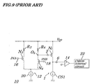
- This small-amplitude interface input circuit 10 comprises: a differential amplifier circuit 12; the level-shifting circuit 1; and a comparator 14.
- the level-shifting circuit 1 is formed together with the following-stage comparator 14 in the same chip, which comparator 14 is supplied with a supply voltage lower than a VDD for the level-shifting circuit 1 (e.g., 1.8V for the comparator 14 versus 3V for the level-shifting circuit), so that the level-shifting circuit 1 is used to shift the level of an input signal to such a range which can be received by the comparator 14.
- the differential amplifier circuit 12 comprises: input terminals 16 and 18; a resistor R3, an n-channel type MOSFET N 3 which has its gate connected to the input terminal 16 and its drain connected via the resistor R 3 to the voltage source V DD ; a resistor R 4 ; an n-channel type MOSFET N 4 which has its gate connected to the input terminal 18 and its drain connected via the resistor R 4 to the voltage source V DD ; and a current source 20 which has its flow-in terminal connected to sources of the n-channel type MOSFETs N 3 and N 4 and its flow-out terminal connected to the ground potential.
- An output terminal O4 of this differential amplifier circuit 12 (i.e., an interconnection point between the resistor R 4 and the source of the n-channel type MOSFET N 4 ) is connected to a gate of an n-channel type MOSFET N 1 .
- the level-shifting circuit 1 has the same configuration as that shown in Fig. 7.
- An output terminal 6 of the level-shifting circuit 1 is connected to an input (+) of the comparator 14.
- a voltage source (not shown) which supplies a reference voltage V CP .
- the comparator has its output connected to a CMOS internal circuit 22.
- the level-shifting circuit 1 acts to output to the comparator 14 such binary signals as corresponding to a binary value represented by two signals INA and INB (both of which are shown in Fig. 10) mutually opposite in phase and different in voltage level which are transmitted via a transmission line and received at the separate input terminals 16 and 18 of the differential amplifier circuit 12.
- the signal INB which is differential-amplified at the differential amplifier circuit 12 is supplied from the output terminal O4 of the differential amplifier circuit 12 to the level-shifting circuit 12 at its input terminal 2, where the INB signal is shifted in level to such a signal V OUT 1 (which is shown in Fig. 10) that can be received by the comparator 14, and then output from the output terminal 6 of the level-shifting circuit 1.
- the comparator 14 sequentially outputs a binary signal having such a waveform as V OUT 2 (1) in Fig. 10, which signal is then processed in the CMOS internal circuit 22.
- FIG. 11 An example of the small-amplitude interface input circuit is shown in Fig. 11.
- This small-amplitude interface input circuit 30 comprises: a differential amplifier circuit 32; a level-shifting circuit 34; and a differential amplifier circuit 36, in such a configuration that the level-shifting circuit 34 has two level-shifting circuits, each of which has the same configuration as that shown in Fig. 7, connected separately to the output terminals O3 and O4 of the differential amplifier circuit 32.
- the differential amplifier circuit 32 has the same configuration as that shown in Fig. 9.
- the level-shifting circuit 34 is configured of two level-shifting circuits each of which is shown in Fig.
- a first level-shifting circuit 34 1 consists of an n-channel type MOSFET N 1 and a constant current source CS1 1
- a second level-shifting circuit 34 2 consists of an n-channel type MOSFET N 2 and a constant current source CS1 2 .
- the level-shifting circuit is formed together with the following-stage differential amplifier circuit 36 in the same chip, which differential amplifier circuit 36 is supplied with a V DD lower than a voltage source for the level-shifting circuit 34 (e.g., 1.8V for the differential amplifier circuit 36 versus 3V for the level-shifting circuit 34), so that the level-shifting circuit 34 is used to shift a signal supplied to the differential amplifier circuit 36 to such a range of level that can be received by the differential amplifier circuit 36.
- a voltage source for the level-shifting circuit 34 e.g., 1.8V for the differential amplifier circuit 36 versus 3V for the level-shifting circuit 34
- V DD voltage source
- this small-amplitude interface input circuit 30 also causes the differential amplifier circuit 36 to output binary signals which correspond to binary values represented by two signals INA and INB mutually opposite in phase and different in voltage level which are received via the transmission line at the input terminals 16 and 18 of the differential amplifier circuit 32.
- the signals INA and INB separately applied at the input terminals 16 and 18 are amplified at the differential amplifier circuit 32 and then respectively applied at gates of the n-channel type MOSFETs N 1 and N 2 of the level-shifting circuit 34.
- an output terminal 6 1 connected to an interconnection point between a source of the n-channel type MOSFET N 1 and the constant current source CS1 1 and an output terminal 6 2 connected to an interconnection point between a source of the n-channel type MOSFET N 2 and the constant current source CS1 2
- signals mutually opposite in phase and different in voltage level which have been shifted in level by as much as a predetermined quantity are output and applied to the (+) and (-) input terminals of the differential amplifier circuit 36 respectively.
- the level-shifting quantity for the signal applied at the (+) input of the differential amplifier circuit 36 is idealistically the same as that for the opposite-phase signal applied at the (-) input and, therefore, two signals which are mutually opposite in phase and different in voltage level are output from the level-shifting circuit 34 and applied to the differential amplifier circuit 36 at its (+) and (-) input terminals, when a level of voltage applied at the (+) input of the differential amplifier circuit is higher than that applied at its (-) input, the differential amplifier circuit 36 provides an output having a higher voltage level and, when a voltage level applied at the (+) input of the differential amplifier circuit 36 is lower than that applied at its (-) input, the differential amplifier circuit 36 provides an output having a lower voltage level.
- binary signals are output from the differential amplifier circuit which correspond to binary values represented by the two signals INA and INB mutually opposite in phase and different in voltage level which are input to the differential amplifier circuit 36 at its input terminals 16 and 18.
- These two signals are held in an idealistic time-wise relationship with the two input signals INA and INB which are mutually opposite in phase and different in voltage level; that is, these two signals have the same signal time-axis width as that of the signals INA and INB, so that even when subjected to signal processing at the CMOS internal circuit 38, these two signals give no inconvenience at all to that signal processing.
- This small-amplitude interface input circuit 40 comprises a level-shifting circuit 42 and a differential amplifier circuit 36.
- the level-shifting circuit 42 consists of two level-shifting circuits 42 1 and 42 2 , each of which has the same configuration as that shown in Fig. 7, in such a configuration that the first level-shifting circuit 42 1 consists of an n-channel type MOSFET N 1 and a constant current source CS1 1 and the second level-shifting circuit 42 2 consists of an n-channel type MOSFET N 2 and a constant current source CS1 2 .
- Two level-shifting circuits are so configured that they are provided, at their respective input terminals 2 1 and 2 2 , with two input signals INA and INB mutually opposite in phase and different in voltage level, via the transmission line, and also that their respective output terminals 6 1 and 6 2 are connected to (-) and (+) inputs of the differential amplifier circuit 36 respectively.
- small-amplitude interface input circuit 40 also causes, like those shown in Figs. 9 and 11, the differential amplifier circuit 36 to output binary signals which correspond to binary values represented by the two input signals INS and INB mutually opposite in phase and different in voltage level which are input to the level-shifting circuits 42 1 and 42 2 at their respective input terminals 2 1 and 2 2 .
- the signals INA and INB applied to the level-shifting circuits 42 1 and 42 2 at their respective input terminals 2 1 and 2 2 are shifted in level at these level-shifting circuits 42 1 and 42 2 respectively, so that the resultant signals which are mutually opposite in phase and different in voltage level are output respectively from the output terminal 6 1 connected to an interconnection point between a source of the n-channel type MOSFET N 1 and the constant current source CS1 1 and the output terminal 6 2 connected to an interconnection point between a source of the n-channel type MOSFET N 2 and the constant current source CS1 2 and applied to the differential amplifier circuit 36 at its (+) and (-) inputs respectively.
- a level-shifting quantity for the signal applied to that differential amplifier circuit at its (+) input is idealistically the same as that for that opposite-phase signal applied at its (-) input and, at the same time, two signals mutually opposite in phase and different in voltage level which are output from the level-shifting circuit 42 are applied to the differential amplifier circuit 36 at its (+) and (-) inputs respectively, when a level of voltage applied to the (+) input is higher than that applied to the (-) input, the differential amplifier circuit 36 outputs a higher level of voltage and, when the level of voltage applied to the (+) input is lower than that applied to the (-) input, the differential amplifier circuit 36 outputs a lower level of voltage.
- the differential amplifier circuit 36 outputs binary signals which correspond to binary values represented by the two signals INA and INB mutually opposite in phase and different in voltage level which are input to the level-shifting circuits 42 1 and 42 2 at their respective input terminals 2 1 and 2 2 .
- These binary signals are held in an idealistic time-wise relationship with the two input signals INA and INB which are mutually opposite in phase and different in voltage level; that is, since these binary signals have the same signal time-axis width as that for the signals INA and INB, they inflict no inconvenience on the CMOS internal circuit when it performs signal processing on them.
- This small amplitude interface output circuit 50 has roughly the same configuration as the small-amplitude interface input circuit 30 shown in Fig. 11.
- the output circuit 50 shown in Fig. 13 is different from the input circuit 30 shown in Fig. 11 in that its level-shifting circuit 34 has its output terminals 6 1 and 6 2 connected to a load resistor 54 via a transmission line 52 and also in that in order to drive the load connected to a bus line at a high speed because of its being an output circuit, its transistors (e.g., n-channel type MOSFETs N 1 , N 2 , N 3 , and N 4 ) have a large size and its constant current values (e.g., those for CS1 1 , CS1 2 , and 20) have a large magnitude.
- its transistors e.g., n-channel type MOSFETs N 1 , N 2 , N 3 , and N 4
- its constant current values e.g., those for CS1 1 , CS1 2 , and 20
- two signals INA and INB mutually opposite in phase and different in voltage level which are separately input at the input terminals 16 and 18 are amplified at the differential amplifier circuit 32 and applied to the gates of the respective n-channel type MOSFETs N1 and N 2 of the level-shifting circuit 34.
- Respectively from the output terminals 6 1 connected to an interconnection point between a source of the n-channel type MOSFET N 1 and the constant current source CS1 1 and the output terminal 6 2 connected to an interconnection point between a source of the n-channel type MOSFET N 2 and the constant current source CS1 2 are output and respectively supplied to a load resistor 54 such signals mutually opposite in phase and different in voltage level which have been shifted in level by a predetermined quantity.
- the load resistor 54 is configured to operate normally when supplied with such a prescribed voltage level of signals.
- the load resistor 54 operates normally as far as the level-shifting quantity given by the level-shifting circuit is not affected by fluctuations in the process nor the temperature.
- Equation 3 V T and ⁇ will vary with fluctuations in the properties and the operating temperature during the manufacturing processes.
- V T 0.5V in the conditions of certain manufacturing processes and operating temperature
- the above-mentioned conventional level-shifting circuits have a disadvantage of not being capable of obtaining a predetermined level-shifting quantity.
- the small-amplitude interface input circuit using this level shifting circuit 1 shown in Fig. 9 also has a problem due to fluctuations in the level-shifting quantity for the level-shifted signal output from the level-shifting circuit 1 which are caused by fluctuations in the manufacturing process, the operating temperature, and the supply voltage.
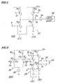
- the level-shifted signal rises in voltage level from V OUT 1S which has an appropriate level-shifting quantity of V OUT 1 shown in Fig. 10 up to V OUT 1U of V OUT 1 shown in the same figure, and is compared, as level-shifted, to the reference voltage V CP at the comparator 14, the comparator 14 outputs such a binary signal as represented by V OUT 2 (2) in Fig. 10.
- output binary signal has a larger signal width than that of a normal signal width (i.e., V OUT 2 (1) in Fig. 10); that is, a skew occurs at the binary signal, thus causing the CMOS internal circuit 22 to malfunction when it has received this signal.
- the level-shifted signal falls in voltage from V OUT 1S which has an appropriate level-shifting quantity of V OUT 1 shown in Fig. 10 down to V OUT 1D of V OUT 1 in the same figure and compared, as level-shifted, to the reference voltage VCP at the comparator 14, the comparator 14 outputs such a binary signal as represented by V OUT 2 (3) shown in Fig. 10.
- output binary signal has a smaller signal width than that of a normal signal (i.e., V OUT 2 (1) in Fig. 10); that is, a skew occurs at the binary signal, thus also causing the CMOS internal circuit to malfunction.
- the small-amplitude interface input circuits shown in Figs. 11 and 12 also suffer from such a skew-related problem as having been described for the small-amplitude interface input circuit 10 shown in Fig. 9, i.e. a problem that fluctuations in the manufacturing process, the operating temperature, and the supply voltage bring about fluctuations in the level-shifting quantity for level-shifted signals output from the level-shifting circuit 1. Since in Figs. 11 and 12 the following-stage is a differential amplifier circuit 36, it does not have such a skew as related to the reference level but does it have such a skew as caused by fluctuations in a so-called off-set voltage.
- the resultant signal as level-shifted would rise or fall from a normal signal level.
- level-shifting quantity between the level-shifting circuits 34 1 and 34 2 as well as between the level-shifting circuits 42 1 and 42 2 , as mentioned above, there occurs a problem of not a skew caused by the reference but a skew caused by fluctuations in the offset voltage.
- CMOS internal circuit may malfunction when it has received such a binary signal as having a skew.
- the small-amplitude interface output circuit shown in Fig. 13 also suffers from such a problem that fluctuations in the level-shifting quantity may cause an output signal having a level-shifting quantity different from the normal level-shifting quantity to be output from the small-amplitude interface output circuit. If such a level-shifting quantity fluctuates, the small-amplitude interface input circuit 50 may malfunction which should operate normally when supplied with an input signal having a prescribed level-shifting quantity, which leads to another disadvantage.
- values of the level-shifting quantity and an input voltage at which the following-stage circuit does not malfunction are obtained beforehand, so that such level-shifting values may be set not to permit that input voltage to be deviated.
- the drain current I DS may be increased and, by the second method, the value of a ⁇ related term, for example, W may be decreased.
- This changing method therefore, is very disadvantageous in adopting in such a field as for example battery-driven integrated circuits, which are strongly required for saving on power dissipation.
- the output impedance of the n-channel MOSFET N 5 is increased, thus deteriorating the high-speed performance, which leads to another disadvantage.
- the second method therefore, cannot be adopted in such integrated circuits which handle high-speed signals.
- the level-shifting quantity can be changed by either of these two changing methods, a problem of fluctuations in the level-shifting quantity caused by fluctuations in the manufacturing process, the operating temperature, or the supply voltage is still left unsolved.
- a level-shifting circuit in which a source of a first insulated-gate transistor is connected with a drain of a second insulated-gate transistor having a same conductivity type as the first insulated-gate transistor, to apply an input signal to a gate of the first insulated-gate transistor in order to output an output signal obtained by level-shifting the input signal by a desired quantity from an interconnection point between the first insulated-gate transistor and the second insulated-gate transistor, wherein
- a preferable mode is one wherein the gate of the second insulated-gate transistor is provided with the constant voltage which is not affected by a variation in a property, an operating temperature, or an operating voltage which is caused by a fluctuation in a manufacturing process for the first insulated-gate transistor and the second insulated-gate transistor.
- a preferable mode is one wherein the two insulated-gate transistors share a same value given by a following Equation 4: (1/T) ⁇ W/L where T is a thickness of a gate insulator film, W is a gate channel width, and L is a gate channel length.
- a preferable mode is one wherein the two insulated-gate transistors shares a value give by a following Equation 5: ⁇ ⁇ ⁇ r ⁇ (S/T) ⁇ W/L where ⁇ is a surface mobility, ⁇ r is a dielectric constant of a gate insulator film, and S is a unit area of a gate channel.
- a preferable mode is one wherein the two insulated-gate transistors are formed on a same substrate, in such a configuration that the constant voltage may be supplied from an outside of the substrate.
- a preferable mode is one wherein the two insulated-gate transistors are formed on a same substrate, in such a configuration that the constant voltage may be an arbitrary constant voltage which is created based on a band-gap reference voltage which is generated in the substrate.
- a preferable mode is one wherein the two insulated-gate transistors are formed on a same substrate, in such a configuration that, in each of the insulated-gate transistors, a source and a back-gate are interconnected.
- a preferable mode is one wherein the two insulated-gate transistors are formed on a same substrate, in such a configuration that, in neither of the insulated-gate transistors, a source and a back-gate are interconnected.
- a preferable mode is one wherein the two insulated-gate transistors are formed on a same substrate, in such a configuration that a back-gate of each of the insulated-gate transistors is clamped to a highest or lowest potential supplied to the substrate.
- an input circuit which shifts a level of a voltage of a signal output from a preceding-stage circuit by as much as a level-shifting quantity to such an input operating level as required by a following-stage circuit which is provided with an operating voltage different from an operating voltage for the preceding-stage circuit, wherein
- a preferable mode is one that wherein has such a configuration that a gate of the second insulated-gate transistor may be provided with the constant voltage which is not affected by a variation in a property or an operating temperature caused by a fluctuation in a manufacturing process of the first insulated-gate transistor and the second insulated-gate transistor.
- a preferable mode is one wherein the two insulated-gate transistors share a same value which is given by a following Equation 6: (1/T) ⁇ W/L
- a preferable mode is one wherein the two insulated-gate transistors share a same value which is given by a following Equation 7: ⁇ ⁇ ⁇ r ⁇ (S/T) ⁇ W/L
- a preferable mode is one wherein the two insulated-gate transistors are formed on a same substrate, in such a configuration that the constant voltage may be supplied from an outside of the substrate.
- a preferable mode is one wherein the two insulated-gate transistors are formed on a same substrate, in such a configuration that the constant voltage may be an arbitrary constant voltage created based on a band-gap reference voltage generated in the substrate.
- a preferable mode is one wherein the two insulated-gate transistors are formed on a same substrate, in such a configuration that in each of the insulated-gate transistors, a source and a back-gate are interconnected.
- a preferable mode is one wherein the two insulated-gate transistors are formed on a same substrate, in such a configuration that in neither of the insulated-gate transistors, a source and a gate are interconnected.
- a preferable mode is one wherein the two insulated-gate transistors are formed on a same substrate, in such a configuration that in each of the insulated-gate transistors, a back-gate is clamped to a highest-level or lowest-level potential supplied to the substrate.
- a preferable mode is one wherein the preceding-stage circuit is a differential amplifier circuit which is supplied with two signals mutually opposite in phase and different in voltage level, to output one output signal to one output terminal, the level-shifting circuit has one input terminal and one output terminal, the following-stage circuit is a comparator which is provided with a reference voltage at one input terminal thereof, the one output of the differential amplifier circuit is connected to one input terminal of the level-shifting circuit, and one output terminal of the level-shifting circuit is connected to the other input terminal of the comparator.
- a preferable mode is one wherein the preceding-stage circuit is a differential amplifier circuit which has two input terminals and two output terminals, the level-shifting circuit has two input terminals and two output terminals, the following-stage circuit is a differential amplifier circuit which has two input terminals, the preceding-stage amplifier circuit is supplied with two input signals opposite in phase and different in voltage level and has two output terminals thereof connected to corresponding input terminals of the level-shifting circuit, and the two output terminals of the level-shifting circuit are connected to corresponding input terminals of the following-stage differential amplifier circuit.
- an input circuit which shifts by a level-shifting quantity a level of a voltage of input signals which is required as an input operating level of an output stage and then supplies a signal thus level-shifted to the output stage, wherein
- a preferable mode is one that wherein has such a configuration that a gate of the second insulated-gate transistor may be provided with the constant voltage which is not affected by a variation in a property or an operating temperature caused by a fluctuation in a manufacturing process for the first insulated-gate transistor and the second insulated-gate transistor.
- a preferable mode is one wherein the two insulated-gate transistors share a same value given by a following Equation 8: (1/T) ⁇ W/L
- a preferable mode is one wherein the two insulated-gate transistors share a same value given by a following Equation 9: ⁇ ⁇ ⁇ r ⁇ (S/T) ⁇ W/L
- a preferable mode is one wherein the two insulated-gate transistors are formed on a same substrate, in such a configuration that the constant voltage may be applied from an outside of the substrate.
- a preferable mode is one wherein the two insulated-gate transistors are formed on a same substrate, in such a configuration that the constant voltage may be an arbitrary constant voltage created based on a band-gap reference voltage generated in the substrate.
- a preferable mode is one wherein the two insulated-gate transistors are formed on a same substrate, in such a configuration that in each of the insulated-gate transistors, a source and a back-gate are interconnected.
- a preferable mode is one wherein the two insulated-gate transistors are formed on a same substrate, in such a configuration that in neither of the insulated-gate transistors, a source and a back-gate are interconnected.
- a preferable mode is one wherein the two insulated-gate transistors are formed on a same substrate, in such a configuration that a back-gate of each of the insulated-gate transistors is clamped to a highest-level or lowest-level potential supplied to the substrate.
- a preferable mode is one wherein the level-shifting circuit has two input terminals provided with two signals opposite in phase and different in voltage level are supplied, and two output terminals, the output stage is a differential amplifier circuit which has two input terminals, and the two output terminals of the level-shifting circuit are connected to corresponding input terminals of the output stage.
- an output circuit which shifts a level of a signal output from an input stage by a predetermined level-shifting quantity and then outputs the signal, wherein
- a preferable mode is one wherein the gate of the second insulated-gate transistor is provided with the constant voltage which is not affected by a variation in a property or an operating temperature caused by a fluctuation in a manufacturing process for the first insulated-gate transistor and the second insulated-gate transistor.
- a preferable mode is one wherein the two insulated-gate transistors share a same value given by a following Equation 1: (1/T) ⁇ W/L
- a preferable mode is one wherein the two insulated-gate transistors share a same value given by a following Equation 11, in such a configuration that a gate of the other insulated-gate transistor may be provided with a constant voltage which is not affected by a fluctuation in a process or a temperature: ⁇ ⁇ ⁇ r (S/T) ⁇ W/L
- a preferable mode is one wherein the two insulated-gate transistors are formed on a same substrate, in such a configuration that the constant voltage may be supplied from an outside of the substrate.
- a preferable mode is one wherein the two insulated-gate transistors are formed on a same substrate, in such a configuration that the constant voltage may be an arbitrary constant voltage created based on a band-gap reference voltage generated in the substrate
- a preferable mode is one wherein the two insulated-gate transistors are formed on a same substrate, in such a configuration that in each of the insulated-gate transistors, a source and a back-gate are interconnected.
- a preferable mode is one wherein the two insulated-gate transistors are formed on a same substrate, in such a configuration that in neither of the insulated-gate transistors, a source and a back-gate are interconnected.
- a preferable mode is one wherein a back-gate of each of the insulated-gate transistors is clamped to a highest-level or lowest-level potential supplied to the substrate.
- a preferable mode is one wherein the input stage is a differential amplifier circuit which has two input terminals and two output terminals, the level-shifting circuit has two input terminals and two output terminals which are connected to two input terminals of a load circuit, and the differential amplifier circuit has the two input terminals thereof supplied with two signals which are mutually opposite in phase and different in voltage level and the two output terminals thereof connected to the two input terminals of the level-shifting circuit.
- a level-shifting circuit that removes the variation factors of the insulated-gate transistors which bring about fluctuations in a level-shifting quantity depending on the manufacturing process, the operating temperature, and the supply voltage, in such a way that during the removal, no factors are allowed to increase power dissipation or deteriorate high-speed performance of the circuit in contrast to the conventional methods for changing the level-shifting quantity.
- that configuration makes it possible to set the level-shifting quantity for the level-shifting circuit in a voltage value, thus arbitrarily changing the level-shifting quantity in voltage.
- the level-shifting quantity for the level-shifting circuit is not dependent on the manufacturing process, the operating temperature, or the supply voltage, so that fluctuations in those factors give no skew to binary signals output from that input circuit, thus preventing a circuit connected to that input circuit from malfunctioning.
- a small-amplitude interface input circuit using the above-mentioned level-shifting circuit has an advantage in such an application field as requiring low power dissipation or high-speed performance.
- a level-shifting quantity for the level-shifting circuit is not dependent on the manufacturing process, the operating temperature, or the supply voltage, so that their fluctuations may not give rise to such output signals mutually opposite in phase and different in voltage level, from that output circuit, that are level-shifted beyond a predetermined level-shifting quantity, thus preventing a load circuit connected to that output circuit from malfunctioning.
- a small-amplitude interface output circuit using the above-mentioned level-shifting circuit has an advantage in such an application field as requiring low power dissipation or high-speed performance.
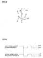
- a level-shifting circuit 1A, Figure 1, in this embodiment, related to a level-shifting circuit capable of outputting an output voltage as shifted by a predetermined level-shifting quantity even with fluctuations in the process or the temperature, comprises: a first input terminal 2; an n-channel type MOSFET N 1 which has its gate connected to the first input terminal 2 and its drain connected to a voltage source V DD ; another n-channel type MOSFET N 2 which has its drain connected to a source of the n-channel type MOSFET N 1 , its gate connected to a second input terminal 4 to be connected to the constant voltage source, and its source connected to the ground; and an output terminal 6 connected to an interconnection point between the source of the n-channel MOSFET N 1 and the drain of the n-channel MOSFET N 2 , in such a configuration that these n-channel MOSFETs N 1 and N 2 are formed on the same substrate.
- a silicon oxide film is used.
- a voltage V R of the constant voltage source is set at such a constant value as not depending on the manufacturing process, the operating temperature, nor the supply voltage.
- the voltage V R may be supplied from an outside of the chip or be an in-chip band-gap voltage or an arbitrary value obtained by stepping up or down that band-gap voltage.
- the n-channel MOSFETs N 1 and N 2 are formed so that their ⁇ 1 and ⁇ 2 values may be equal to each other.
- the ⁇ 1 value of the n-channel MOSFET N 1 is given by the following Equation 12 and
- n-channel MOSFETs N 1 and N 2 each have their back gates (region for forming elements therein) and sources connected to each other.
- V GS ⁇ 2I DS / ⁇ 2 ⁇ 1/2 + V T
- V R is set at a value which is not dependent on the manufacturing process, the operating temperature, nor the supply voltage, the V OUT also does not vary with them. That is, a level-shifting quantity for the level-shifting circuit 1A does not vary with the manufacturing process, the operating temperature, nor the supply voltage.
- the output voltage V OUT provided from the level-shifting circuit 1A can be output as a voltage not dependent on the manufacturing process, the operating temperature, nor the supply voltage. That is, even if the manufacturing process, the operating temperature, or the supply voltage may fluctuate, the output voltage V OUT having no fluctuations in the level-shifting quantity can be output from the level-shifting circuit 1A.
- the level-shifting quantity can be adjusted at an arbitrary set-point value by adjusting the constant voltage V R .
- that setting need not change a current flowing through the NMOS transistors nor the gate width W, thus inflicting, unlike the conventional embodiments, no disadvantage which brings about increases in power dissipation or deterioration in high-speed performance of the level-shifting circuit.
- the level-shifting circuit according to this embodiment brings about no fluctuations in the level-shifting quantity even with fluctuations in the manufacturing process, the operating temperature, or the supply voltage, thus making it possible to output a value of 1.5V from itself, which is originally a desired output V OUT .
- the level-shifting circuit 1A (Fig. 1) used in the first embodiment is applied to shift the level of a voltage between a differential amplifier circuit 12 and a comparator 14 in a small-amplitude interface input circuit 10A, in order to match a voltage level of a signal output from the input-stage differential amplifier circuit 12 with a voltage level of a signal input to the output-stage comparator in the small-amplitude interface input circuit 10A.
- level-shifting circuit 1A is formed together with the following-stage comparator 14 in the same chip and that comparator 14 is supplied with a V DD lower than a supply voltage for the level-shifting circuit 1A (e.g., 1.8V for the comparator 14 versus 3V for the level-shifting circuit 1A), that level-shifting circuit 1A is used to shift the level of an input signal to such a range of level that can be received by that comparator 14.
- a supply voltage for the level-shifting circuit 1A e.g., 1.8V for the comparator 14 versus 3V for the level-shifting circuit 1A
- the small-amplitude interface input circuit 10A in this embodiment comprises: a differential amplifier circuit 12 which receives at its separate input terminals such two signals transmitted via a transmission line that are mutually opposite in phase and different in voltage level; a level-shifting circuit 1A; and a comparator 14.
- the differential amplifier circuit 12 of the level-shifting circuit 1A and the comparator 14 of the small-amplitude interface input circuit 10A are the same as those described with reference to Fig. 9, while the level-shifting circuit 1A is the same as that described with reference to Fig. 1.
- the differential amplifier circuit 12 receives at its input terminals 16 and 18 such two input signals INA and INB (which are shown in Fig. 10) which are mutually opposite in phase and different in voltage level. Then, the signal INB as differential-amplified is output from an output terminal O4 of the differential amplifier circuit 12. That signal INB is applied to the level-shifting circuit 1A at its input terminal 2.
- the level-shifting circuit 1A outputs a signal as level-shifted from its output terminal 6.
- the level-shifting quantity given by the level-shifting circuit 1A is enough, like in the case of the circuit shown in Fig. 9, to permit the concerned level of a signal input at the level-shifting circuit 1A to be received by the comparator 14.
- level shifting by that level-shifting circuit 1A are not dependent on the manufacturing process, the operating temperature, nor the supply voltage.
- the signal output from the level-shifting circuit 1A is shifted by such a level-shifting quantity that it may not be dependent on the manufacturing process, the operating temperature, nor the supply voltage. Since such signal is supplied to the comparator 14 at its (-) input terminal, such a binary signal can be output from the comparator 14 as a skew-free binary signal that corresponds to the two input signals INA and INB mutually opposite in phase and different in voltage level, even if there are fluctuations in the manufacturing process, the operating temperature, or the supply voltage of the n-channel type MOSFETs N 1 and N 2 which compose the level-shifting circuit 1A.
- a signal input to the comparator 14 at its (-) input terminal is not stepped up or down in voltage like V OUT 1U or V OUT 1D shown in Fig. 10 by fluctuations in a level-shifting quantity of signals output from the level-shifting circuit 1A caused by fluctuations in the manufacturing process, the operating temperature, or the supply voltage, thus making it possible to supply a skew-free binary signal from the comparator 14 to a CMOS internal circuit 22.
- the level-shifting quantity can be adjusted to an arbitrary set-point value by adjusting the constant voltage V R .
- that setting need not change a current flowing through the NMOS transistors or the gate width W, thus inflicting, unlike the conventional embodiments, no disadvantage which brings about increases in power dissipation or deterioration in high-speed performance of the level-shifting circuit 1A.
- the level-shifting circuit 1A used in the first embodiment is applied between an input-stage differential amplifier circuit and an output-stage differential amplifier circuit in a small-amplitude interface input circuit, in order to match a voltage level of a signal output from the input-stage differential amplifier circuit with a voltage level of a signal input to the output-stage differential amplifier circuit.
- the level-shifting circuit 1B is used to shift the level of a signal supplied to the differential amplifier circuit 36 to such a range of level that can be received by the differential amplifier circuit 36.
- the small-amplitude interface input circuit 30A in this embodiment comprises: a differential amplifier circuit 32 which received at its separate input terminals such two input signals transmitted via the transmission line that are mutually opposite in phase and different in voltage level; a level-shifting circuit 1B which is connected with two input terminals 21 and 22 which respectively correspond to two output terminals of the differential amplifier circuit 32; and another differential amplifier circuit 36 which are connected with input terminals which respectively correspond to two output terminals 6 1 and 6 2 of the level-shifting circuit 1B.
- the differential amplifier circuits 32 and 36 are the same as those described with reference to Fig. 11.
- a first level-shifting circuit 1B1 and a second level-shifting circuit 1B2 which compose the level-shifting circuit 1B are of the same configuration as that shown in Fig. 1, so that they are discriminated from each other by adding subscripts 1 and 2 to n-channel type MOSFETs composing the first and second level-shifting circuits 1B1 and 1B2 respectively; therefore, the description of these two level-shifting circuits 1B1 and 1B2 is omitted here.
- An output terminal O3 of the differential amplifier circuit 32 is connected to the input terminal 21 of the first level-shifting circuit 1B1 and its output terminal O4, to the input terminal 22 of the second level-shifting circuit 1B2.
- the output terminal 6 1 of the first level-shifting circuit 1B1 is connected to the (+) input terminal of the differential amplifier circuit 36 and the output terminal 6 2 of the second level-shifting circuit 1B2, to the (-) input terminal of the differential amplifier circuit 36.
- Two input signals INA and INB mutually opposite in phase and different in voltage level which are transmitted via the transmission line are input to the differential amplifier circuit 32 at its input terminals 16 and 18 separately. These signals INA and INB are amplified at the differential amplifier circuit 32 and then applied to the gate of the n-channel type MOSFETs N11 and N21 of the levels-shifting circuit 1B respectively.
- a level-shifting quantity for signals output as level-shifted from the output terminals 6 1 and 6 2 of the level-shifting circuits 1B1 and 1B2 respectively is enough, like in the case of the circuit shown in Fig. 11, to permit the concerned level of a signal input at the level-shifting circuits 1B1 and 1B2 to be received by the differential amplifier circuit 36.
- a level-shifting quantity by the level-shifting circuits 1B1 and 1B2 of that level-shifting circuit 1B are not dependent on the process or the temperature.
- the respective signals output from the separate level-shifting circuits 1B1 and 1B2 of the level-shifting circuit 1B are shifted by such a level-shifting quantity that they may not be dependent on the manufacturing process, the operating temperature, nor the supply voltage.
- such a binary signal can be output from the differential amplifier circuit 36 as a skew-free binary signal that corresponds to the two input signals INA and INB mutually opposite in phase and different in voltage level, even if there are fluctuations in the manufacturing process, the operating temperature, or the supply voltage of the n-channel type MOSFETs N 11 , N 12 , N 21 , and N 22 which compose the level-shifting circuit.
- signals applied to the (+) and (-) input terminals of the differential amplifier circuit 36 are not stepped up or down in voltage like V OUT 1U or V OUT 1D shown in Fig. 10 by fluctuations in level-shifting quantity of signals output from the level-shifting circuit 34 caused by fluctuations in the manufacturing process, the operating temperature, or the supply voltage, thus making it possible to supply a skew-free binary signal from the differential amplifier circuit 36 to the CMOS internal circuit 38.
- the level-shifting quantity can be adjusted to an arbitrary set-point value by adjusting the constant voltage VR.
- that setting need not change a current flowing through the NMOS transistors or the gate width W, thus inflicting, unlike the conventional embodiments, no disadvantage which brings about increases in power dissipation or deterioration in high-speed performance of the level-shifting circuit.
- the level-shifting circuit used in the first embodiment is applied between each input terminal of a small-amplitude interface input circuit and the corresponding input terminal of an output-stage differential amplifier circuit, in order to match a voltage level of two input signals mutually opposite in phase and different in voltage level which are input via the transmission line to the small-amplitude interface input circuit at its two input terminals with a voltage level of signals input to the output-stage differential amplifier circuit at its respective input terminals.
- a level-shifting circuit 1C See Fig.
- the small-amplitude interface input circuit 40A in this embodiment comprises: a level-shifting circuit 1C which receives at its separate input terminals such two input signals that are mutually opposite in phase and different in voltage level; and a differential amplifier circuit 36 which are connected with input terminals which correspond to two output terminals of the level-shifting circuit 1C.
- That differential amplifier circuit 36 is the same as that described with reference to Fig. 11.
- a fist level-shifting circuit 1C1 and a second level-shifting circuit 1C2, which compose the level-shifting circuit 1C, are of the same configuration as that shown in Fig. 1, so that they are discriminated from each other by adding subscripts 1 and 2 to n-channel MOSFETs composing the first and second level-shifting circuits 1C1 and 1C2 respectively; therefore, the description of these two level-shifting circuits 1C1 and 1C2 is omitted here.
- One of the two input terminals which receive via the transmission line such two input signals that are opposite in phase and different in voltage level acts also as the input terminal 2 1 of the fist level-shifting circuit 1C1, while the other input terminal acts as the input terminal 2 2 of the second level-shifting circuit 1C2.
- the output terminal 6 1 of the first level-shifting circuit 1C1 is connected to the differential amplifier circuit 36 at its (+) input terminal
- the output terminal 6 2 of the second level-shifting circuit 1C2 is connected to the differential amplifier circuit 36 at its (-) input terminal.
- Two input signals INA and INB mutually opposite in phase and different in voltage level which are transmitted via the transmission line are applied to the level-shifting circuit 1C at its input terminals 2 1 and 2 2 separately. Then, two signals mutually opposite in phase and different in voltage level which are shifted by the respective same predetermined level-shifting quantity are output from the output terminal 6 1 of the level-shifting circuit 1C1 and the output terminal 6 2 of the level-shifting circuit 1C2 respectively.
- the level-shifting quantity for signals output as level-shifted from the output terminals 6 1 and 6 2 respectively of the level-shifting circuits 1C1 and 1C2 of the level-shifting circuit 1C is enough, like in the case of the circuit shown in Fig. 12, to the concerned level of a signal input at the level-shifting circuits 1C1 and 1C2 to be received by the differential amplifier circuit 36.
- level shifting by the level-shifting circuits 1C1 and 1C2 of that level-shifting circuit 1C are not dependent on the process or the temperature.
- the respective signals output from the separate level-shifting circuits 1C1 and 1C2 of the level-shifting circuit 1C are shifted by such a level-shifting quantity that they may not be dependent on the manufacturing process, the operating temperature, nor the supply voltage.
- such a binary signal can be output from the differential amplifier circuit 36 as a skew-free binary signal that corresponds to the two input signals INA and INB which are mutually opposite in phase and different in voltage level, even if there are fluctuations in the manufacturing process, the operating temperature, or the supply voltage of the n-channel MOSFETs N 11 , N 12 , N 21 , and N 22 which compose the level-shifting circuit.
- signals applied to the (+) and (-) input terminals of the differential amplifier circuit 36 are not stepped up or down in voltage like V OUT 1U or V OUT 1D shown in Fig. 10 just because of fluctuations in the level-shifting quantity of signals output from the level-shifting circuit 42 caused by fluctuations in the manufacturing process, the operating temperature, or the supply voltage, thus making it possible to supply a skew-free binary signal from the differential amplifier circuit 36 to the CMOS internal circuit 38.
- the level-shifting quantity can be adjusted to an arbitrary set-point value by adjusting the constant voltage V R .
- that setting need not change a current flowing through the NMOS transistors or the gate width W, thus inflicting, unlike the conventional embodiments, no disadvantage which brings about increases in power dissipation or deterioration in high-speed performance of the level-shifting circuit.
- the level-shifting circuit 1A used in the first embodiment is applied between an input-stage differential amplifier circuit 32 and a load resistor 54 of a small-amplitude interface output circuit 50A, in order to match a voltage level of a signal output from the input-stage differential amplifier circuit 32 with a voltage level of a signal supplied to the load resistor 54.
- This small-amplitude interface output circuit 50A in this embodiment comprises: the differential amplifier circuit 32 which receives at its separate input terminals 16 and 18 such input signals that are mutually opposite in phase and different in voltage level; and a level-shifting circuit 1B which is connected with input terminals 2 1 and 2 2 which correspond to two output terminals O 3 and O 4 of the differential amplifier circuit 32, in such a configuration that the two output terminals 6 1 and 6 2 of the level-shifting circuit 1B are connected to the transmission line 52.
- the differential amplifier circuit 32 is the same as that described with reference to Fig. 11 and the level-shifting circuit 1B, the same as that described with reference with Fig. 4.
- Two input signals INA and INB mutually opposite in phase and different in voltage level are applied to the differential amplifier circuit at its input terminals 16 and 18 respectively.
- These signals INA and INB are amplified at the differential amplifier circuit 32 and then applied to the gate of the n-channel MOSFETs N 11 and N 21 of the level-shifting circuit 1B respectively.
- the level-shifting quantity for signals output as level-shifted from the output terminals 6 1 and 6 2 of the first and second level-shifting circuits 1B1 and 1B2 respectively is enough to permit the level of signals input at the respective level-shifting circuits 1B1 and 1B2 of the level-shifting circuit 1B to be received by the load resistor 54, as specified in terms of level.
- level shifting by these respective level-shifting circuits 1B1 and 1B2 of the level-shifting circuit 1B are not dependent on the manufacturing process, the operating temperature, not the supply voltage.
- the load circuit 54 can be supplied with a signal having a specified level-shifting quantity, thus being prevented from malfunctioning.
- the level-shifting quantity can be adjusted to an arbitrary set-point value by adjusting the constant voltage V R .
- that setting need not change a current flowing through the NMOS transistors or the gate width W, thus inflicting, unlike the conventional embodiments, no disadvantage which brings about increases in power dissipation or deterioration in high-speed performance of the level-shifting circuit.
- p-channel type MOSFETs may be used in those embodiments.
- back-gate and the source are interconnected in the above-mentioned embodiments, they may not be interconnected within a tolerable fluctuation range of the level-shifting quantity.
Landscapes
- Engineering & Computer Science (AREA)
- Computer Hardware Design (AREA)
- Physics & Mathematics (AREA)
- Computing Systems (AREA)
- General Engineering & Computer Science (AREA)
- Mathematical Physics (AREA)
- Logic Circuits (AREA)
- Electronic Switches (AREA)
Applications Claiming Priority (2)
| Application Number | Priority Date | Filing Date | Title |
|---|---|---|---|
| JP35659198A JP3171177B2 (ja) | 1998-12-15 | 1998-12-15 | レベルシフト回路、該レベルシフト回路を用いた入力回路及び出力回路 |
| JP35659198 | 1998-12-15 |
Publications (2)
| Publication Number | Publication Date |
|---|---|
| EP1014585A2 true EP1014585A2 (de) | 2000-06-28 |
| EP1014585A3 EP1014585A3 (de) | 2001-12-19 |
Family
ID=18449797
Family Applications (1)
| Application Number | Title | Priority Date | Filing Date |
|---|---|---|---|
| EP99124947A Withdrawn EP1014585A3 (de) | 1998-12-15 | 1999-12-14 | Pegelverschiebungsschaltung und diese verwendende Ein- und Ausgangsschaltungen |
Country Status (5)
| Country | Link |
|---|---|
| US (1) | US6288580B1 (de) |
| EP (1) | EP1014585A3 (de) |
| JP (1) | JP3171177B2 (de) |
| KR (1) | KR100354672B1 (de) |
| CN (1) | CN1259798A (de) |
Families Citing this family (4)
| Publication number | Priority date | Publication date | Assignee | Title |
|---|---|---|---|---|
| JP4047178B2 (ja) | 2003-01-06 | 2008-02-13 | 富士通株式会社 | 入力回路 |
| US9407259B2 (en) * | 2014-06-27 | 2016-08-02 | Finisar Corporation | Driver circuit |
| CN108134601B (zh) * | 2016-11-30 | 2021-08-06 | 上海复旦微电子集团股份有限公司 | 接口电路 |
| JP2019033386A (ja) * | 2017-08-08 | 2019-02-28 | 株式会社村田製作所 | 差動増幅回路 |
Citations (2)
| Publication number | Priority date | Publication date | Assignee | Title |
|---|---|---|---|---|
| US4814635A (en) | 1987-11-27 | 1989-03-21 | Motorola, Inc. | Voltage translator circuit |
| JPH03291013A (ja) | 1990-04-09 | 1991-12-20 | Sumitomo Electric Ind Ltd | レベルシフト回路 |
Family Cites Families (12)
| Publication number | Priority date | Publication date | Assignee | Title |
|---|---|---|---|---|
| JPS5550743A (en) * | 1978-10-11 | 1980-04-12 | Fujitsu Ltd | Level shift circuit |
| US4714840A (en) * | 1982-12-30 | 1987-12-22 | Thomson Components - Mostek Corporation | MOS transistor circuits having matched channel width and length dimensions |
| US4717836A (en) * | 1986-02-04 | 1988-01-05 | Burr-Brown Corporation | CMOS input level shifting circuit with temperature-compensating n-channel field effect transistor structure |
| JP2751422B2 (ja) * | 1988-06-27 | 1998-05-18 | 日本電気株式会社 | 半導体装置 |
| JP2666435B2 (ja) * | 1988-11-30 | 1997-10-22 | 日本電気株式会社 | 温度補償レベルシフト回路 |
| JPH0327619A (ja) * | 1989-06-23 | 1991-02-06 | Sumitomo Electric Ind Ltd | レベルシフト回路 |
| JPH06260925A (ja) * | 1993-03-03 | 1994-09-16 | Nec Ic Microcomput Syst Ltd | レベルシフト回路 |
| JPH0818433A (ja) * | 1994-06-29 | 1996-01-19 | Matsushita Electric Ind Co Ltd | レベルシフト回路 |
| US5656952A (en) * | 1995-11-13 | 1997-08-12 | Analog Devices, Inc. | All-MOS differential high speed output driver for providing positive-ECL levels into a variable load impedance |
| JP3307547B2 (ja) * | 1996-10-30 | 2002-07-24 | 富士通株式会社 | レベルシフト回路及びこれを用いた電圧制御型発振回路 |
| US5786724A (en) * | 1996-12-17 | 1998-07-28 | Texas Instruments Incorporated | Control of body effect in MOS transistors by switching source-to-body bias |
| KR100246335B1 (ko) * | 1997-03-22 | 2000-03-15 | 김영환 | 메모리소자의내부정전압회로 |
-
1998
- 1998-12-15 JP JP35659198A patent/JP3171177B2/ja not_active Expired - Fee Related
-
1999
- 1999-12-10 US US09/458,056 patent/US6288580B1/en not_active Expired - Lifetime
- 1999-12-14 EP EP99124947A patent/EP1014585A3/de not_active Withdrawn
- 1999-12-14 KR KR1019990057471A patent/KR100354672B1/ko not_active Expired - Fee Related
- 1999-12-15 CN CN99127833A patent/CN1259798A/zh active Pending
Patent Citations (2)
| Publication number | Priority date | Publication date | Assignee | Title |
|---|---|---|---|---|
| US4814635A (en) | 1987-11-27 | 1989-03-21 | Motorola, Inc. | Voltage translator circuit |
| JPH03291013A (ja) | 1990-04-09 | 1991-12-20 | Sumitomo Electric Ind Ltd | レベルシフト回路 |
Also Published As
| Publication number | Publication date |
|---|---|
| CN1259798A (zh) | 2000-07-12 |
| JP3171177B2 (ja) | 2001-05-28 |
| JP2000183723A (ja) | 2000-06-30 |
| KR20000048133A (ko) | 2000-07-25 |
| EP1014585A3 (de) | 2001-12-19 |
| US6288580B1 (en) | 2001-09-11 |
| KR100354672B1 (ko) | 2002-10-04 |
Similar Documents
| Publication | Publication Date | Title |
|---|---|---|
| US4477737A (en) | Voltage generator circuit having compensation for process and temperature variation | |
| US6801064B1 (en) | Buffer circuit using low voltage transistors and level shifters | |
| KR0136233B1 (ko) | 인터페이스 회로 | |
| US6791391B2 (en) | Level shifting circuit | |
| EP1229649B1 (de) | Ausgangsschaltung | |
| JPH07183774A (ja) | 出力バッファ回路、入力バッファ回路、および入出力バッファ回路 | |
| US7391276B2 (en) | Oscillation apparatus capable of compensating for fluctuation of oscillation frequency | |
| US7078934B2 (en) | Level conversion circuit | |
| JP3240042B2 (ja) | 半導体出力回路 | |
| US5847581A (en) | Low power CMOS precision input receiver with integrated reference | |
| US20030020516A1 (en) | Voltage comparator circuit and substrate bias adjusting circuit using same | |
| US7579882B2 (en) | Output buffer circuit eliminating high voltage insulated transistor and level shift circuit, and an electronic device using the output buffer circuit | |
| US12341498B2 (en) | Bidirectional signal conversion circuit | |
| US6853236B1 (en) | Circuit apparatus operable under high voltage | |
| US20060061395A1 (en) | Semiconductor integrated circuit | |
| US6556040B2 (en) | Method and apparatus for non-linear termination of a transmission line | |
| US6288580B1 (en) | Level-shifting circuit and input and output circuits using the same | |
| EP1585278A2 (de) | Daten-Ausgangstreiber mit verbessertem Überspannungsschutz | |
| EP0651511A2 (de) | Halbleiterschaltungsanordnung mit einer Kombination von CMOS- und bipolaren Schaltungen | |
| JPH098637A (ja) | 半導体装置 | |
| US7532071B2 (en) | Operational amplifier circuit | |
| EP0868026A1 (de) | Schaltung mit veränderlicher Verzögerung | |
| US7737734B1 (en) | Adaptive output driver | |
| US6801069B1 (en) | Receiving latch with hysteresis | |
| US7064586B2 (en) | Input buffer circuit including reference voltage monitoring circuit |
Legal Events
| Date | Code | Title | Description |
|---|---|---|---|
| PUAI | Public reference made under article 153(3) epc to a published international application that has entered the european phase |
Free format text: ORIGINAL CODE: 0009012 |
|
| AK | Designated contracting states |
Kind code of ref document: A2 Designated state(s): AT BE CH CY DE DK ES FI FR GB GR IE IT LI LU MC NL PT SE Kind code of ref document: A2 Designated state(s): DE FR GB |
|
| AX | Request for extension of the european patent |
Free format text: AL;LT;LV;MK;RO;SI |
|
| PUAL | Search report despatched |
Free format text: ORIGINAL CODE: 0009013 |
|
| AK | Designated contracting states |
Kind code of ref document: A3 Designated state(s): AT BE CH CY DE DK ES FI FR GB GR IE IT LI LU MC NL PT SE |
|
| AX | Request for extension of the european patent |
Free format text: AL;LT;LV;MK;RO;SI |
|
| RIC1 | Information provided on ipc code assigned before grant |
Free format text: 7H 03K 19/0185 A, 7H 03K 19/003 B, 7H 03K 19/0944 B |
|
| 17P | Request for examination filed |
Effective date: 20011127 |
|
| AKX | Designation fees paid |
Free format text: DE FR GB |
|
| RAP1 | Party data changed (applicant data changed or rights of an application transferred) |
Owner name: NEC ELECTRONICS CORPORATION |
|
| 17Q | First examination report despatched |
Effective date: 20080822 |
|
| RAP1 | Party data changed (applicant data changed or rights of an application transferred) |
Owner name: RENESAS ELECTRONICS CORPORATION |
|
| RAP1 | Party data changed (applicant data changed or rights of an application transferred) |
Owner name: RENESAS ELECTRONICS CORPORATION |
|
| RAP1 | Party data changed (applicant data changed or rights of an application transferred) |
Owner name: RENESAS ELECTRONICS CORPORATION |
|
| STAA | Information on the status of an ep patent application or granted ep patent |
Free format text: STATUS: EXAMINATION IS IN PROGRESS |
|
| STAA | Information on the status of an ep patent application or granted ep patent |
Free format text: STATUS: THE APPLICATION IS DEEMED TO BE WITHDRAWN |
|
| 18D | Application deemed to be withdrawn |
Effective date: 20170701 |