EP1014592A2 - Mobilfunkendgerät und Oberflächewellenantenneduplexer - Google Patents
Mobilfunkendgerät und Oberflächewellenantenneduplexer Download PDFInfo
- Publication number
- EP1014592A2 EP1014592A2 EP99124880A EP99124880A EP1014592A2 EP 1014592 A2 EP1014592 A2 EP 1014592A2 EP 99124880 A EP99124880 A EP 99124880A EP 99124880 A EP99124880 A EP 99124880A EP 1014592 A2 EP1014592 A2 EP 1014592A2
- Authority
- EP
- European Patent Office
- Prior art keywords
- transmitting
- receiving
- signal
- saw
- terminal
- Prior art date
- Legal status (The legal status is an assumption and is not a legal conclusion. Google has not performed a legal analysis and makes no representation as to the accuracy of the status listed.)
- Withdrawn
Links
Images


Classifications
-
- H—ELECTRICITY
- H03—ELECTRONIC CIRCUITRY
- H03H—IMPEDANCE NETWORKS, e.g. RESONANT CIRCUITS; RESONATORS
- H03H9/00—Networks comprising electromechanical or electro-acoustic elements; Electromechanical resonators
- H03H9/02—Details
- H03H9/05—Holders or supports
- H03H9/0538—Constructional combinations of supports or holders with electromechanical or other electronic elements
- H03H9/0566—Constructional combinations of supports or holders with electromechanical or other electronic elements for duplexers
- H03H9/0576—Constructional combinations of supports or holders with electromechanical or other electronic elements for duplexers including surface acoustic wave [SAW] devices
-
- H—ELECTRICITY
- H03—ELECTRONIC CIRCUITRY
- H03H—IMPEDANCE NETWORKS, e.g. RESONANT CIRCUITS; RESONATORS
- H03H9/00—Networks comprising electromechanical or electro-acoustic elements; Electromechanical resonators
- H03H9/70—Multiple-port networks for connecting several sources or loads, working on different frequencies or frequency bands, to a common load or source
- H03H9/72—Networks using surface acoustic waves
- H03H9/725—Duplexers
Definitions
- the present invention relates to a dual-band/triple-band mobile radio terminal, a surface acoustic wave (hereinafter referred to as "SAW") filter suitable for such a mobile radio terminal, or an antenna duplexer constituted by such an SAW filter and a high-frequency switch.
- SAW surface acoustic wave
- a single antenna is shared between transmission and reception through an antenna duplexer so as to transmit and receive transmission/reception signals adapted to a mobile communication system.
- a related-art antenna duplexer has a receiving dielectric resonator using a receiving frequency band as its passing frequency band, and a transmitting dielectric resonator using a transmitting frequency band as its passing frequency band.
- a matching circuit and a phase shift circuit are combined in order to prevent and reduce interference of the receiving and transmitting dielectric resonators with each other.
- Fig. 2 shows a circuit block diagram of such an antenna duplexer for a GSM system mobile radio terminal.
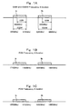
- Fig. 1A shows a frequency allocation of a GSM system.
- a receiving frequency band f R ranges from 935 to 960 MHz, and a transmitting frequency band f T ranges from 890 to 915 MHz.
- An antenna duplexer 1 is connected to an antenna 2 through an antenna terminal 3 shared by a receiving system and a transmitting system.
- a reception signal supplied from the antenna 2 is supplied to the receiving system through the terminal 3 and a parallel connection point 4 which connects the receiving and transmitting systems.
- the reception signal is supplied to a receiving-system terminal 9 while desired receiving frequency characteristics are ensured.
- the receiving system includes an SAW filter 7 using the receiving frequency band f R as its passing frequency band, a matching circuit 6-1 for impedance-matching of the SAW filter 7, and a phase shift circuit 5-1 for suppressing leakage of a transmission signal into the receiving system.
- the transmission signal is supplied to the transmitting system through a transmitting-system terminal 10, and then supplied to the antenna 2 through the parallel connection point 4 and the terminal 3 while desired transmitting frequency characteristics are ensured.
- the transmitting system includes an SAW filter 8 using the transmitting frequency band f T as its passing frequency band, a matching circuit 6-2 for impedance-matching of the SAW filter 8, and a phase shift circuit 5-2 for suppressing leakage of the reception signal into the transmitting system.
- such an antenna duplexer used a dielectric single-layer substrate in which a signal pattern was formed on its upper surface and a ground pattern was formed on its lower surface, while elements constituting the SAW filters, phase shift circuits and matching circuits were mounted on its upper surface.
- a low-noise modulation system such as an off-set PLL modulation system is adopted and a transmitting system of an antenna duplexer is formed by a switch so that a mobile radio terminal suitable as a dual-band/triple-band one is realized.
- a transmitting system is shared by two mobile communication systems having transmitting frequency bands close to each other.
- a multi-layer substrate is adopted, and matching circuits and so on are formed by lumped-constant circuit elements, and the SAW filter is received in a space provided in the multi-layer substrate.
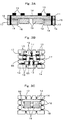
- Figs. 3A to 3C are a sectional view, a top view and a bottom view of the antenna duplexer respectively.
- This embodiment uses a dielectric multi-layer substrate in which first and second dielectric substrates (upper and lower dielectric substrates) 11 and 12 are bonded with each other through a bonding agent 15.
- Lumped-constant circuit elements 13 chips capacities, chip inductors, helical coils, etc. constituting phase shift circuits and matching circuits are mounted on the upper surface of the upper dielectric substrate 11 (the uppermost surface of the dielectric multi-layer substrate).
- a space is provided in a portion of the lower dielectric substrate 12 so as to receive SAW filters 16.
- Solder-coated portions (soldering lands) 55 for mounting the lumped-constant circuit elements 13 thereon are provided on the upper surface of the upper dielectric substrate 11, and soldering lands 55 for mounting the SAW filters 16 thereon are provided on the lower surface of the upper dielectric substrate 11.
- a signal terminal or ground terminal pattern 18 is provided on the lower surface of the lower dielectric substrate 12 (the lowermost surface of the dielectric multi-layer substrate) so as to be connected with signal lines and the ground on a board (not shown).
- the circuit pattern on the upper surface of the upper dielectric substrate 11 is electrically connected with the SAW filters 16 and the terminal pattern on the lower surface of the lower dielectric substrate 12 through conductors in through holes 14 and castellations 17.
- Glass epoxy resin which is rich in degree of freedom of working and inexpensive in cost is suitable for the multi-layer substrate. Glass ceramic or the like may be also used.
- the SAW filters large in volume are built in the multi-layer substrate, and the lumped-constant circuit elements constituting matching circuits, phase shift circuits, and so on are disposed on the upper surface of the multi-layer substrate, so that the SAW antenna duplexer can be made smaller in size than a related-art SAW duplexer in which SAW filters and other elements are mounted on a single-layer substrate.
- the lumped-constant circuit elements mounted on the upper surface of the upper dielectric substrate 11 are not limited to the phase shift circuits and matching circuits.
- the following embodiment will show an antenna duplexer using switching elements such as pin diodes, gallium arsenide ICs, etc.
- the antenna duplexer is suitable for a dual-mode/triple-mode mobile radio terminal.
- Those switching elements and bias circuits for driving the switching elements are also constituted by lumped-constant circuit elements, and the lumped-constant circuit elements are mounted on the upper surface of the upper dielectric substrate 11.
- the increase of the volume can be suppressed also in a large-circuit-scale antenna duplexer for a dual-mode/triple-mode mobile radio terminal.
- the upper surface of the upper dielectric substrate mounted with lumped-constant circuit elements, switching elements and so on is covered with a metal cap 43 from above.
- the metal cap 43 is connected with the ground pattern provided on the upper surface of the upper dielectric substrate.
- the connection is provided at one or more places of the metal cap 43 through solder or the like 44.
- each mounted SAW filter is an SAW filter 46 received in a sheet-mounted package.
- the SAW filter received in a sheet-mounted package ensures the air-tightness, and makes the working of handling the SAW filter easy.
- Fig. 9 shows an example in which SAW filter chips 47 are mounted on the SAW filters respectively with bumps 48 of gold, aluminum or the like by a flip-chip bonding method. This example is advantageous in reduction of area, thickness and cost.
- the SAW filter chips 47 are fixed to the substrate surface through a conductive or non-conductive bonding agent 50 while signal and ground patterns on the SAW filter chips 47 are electrically connected with the signal and ground patterns formed on the substrate surface through wires 49 of aluminum or the like.
- This example is advantageous in reduction of area, thickness and cost.
- the space to receive the SAW filters provided on the multi-layer substrate is covered with a cover 52 of metal, resin or ceramic.
- the protection of the SAW filters can be reinforced.
- a part or all of the chip inductors and helical coils are replaced by spiral coils 53 formed on the lower surface of the upper dielectric substrate or the upper surface of the lower dielectric substrate.
- the thickness of the bonding agent 15 bonding the upper and lower dielectric substrates 11 and 12 can be used effectively, and helical coils and so on can be eliminated from the upper surface of the upper dielectric substrate.
- the SAW antenna duplexer can be made thin.
- the number of coils mounted on the upper surface of the upper dielectric substrate is reduced. As a result, the antenna duplexer can be made low in cost.
- intermediate dielectric substrates 54 are provided between the upper and lower dielectric substrates. That is, the multi-layer substrate in this embodiment is not limited to one constituted by two dielectric substrates bonded with each other. In this case, the spiral coils 53 shown in the example of Fig. 13 are further provided on the intermediate dielectric substrates 54. Thus, a large number of spiral coils can be formed more advantageously in miniaturization.
- ETACS Extended Total Access Communication System
- FDMA Frequency Division Multiple Access
- GSM Global System for Mobile Communication
- EGSM Extended Global System for Mobile Communication
- PCN Personal Communication Network
- TDMA Time Division Multiple Access
- North America is served by EAMPS (Extended Advanced Mobile Phone Service) which is an FDMA system and PCS (Personal Communication System) which is a TDMA system.
- NTACS New Total Access Communication System
- PDC Personal Digital Cellular
- a user can receive service from a plurality of systems through a single mobile radio terminal.
- Fig. 1 shows the frequency allocation of transmitting/receiving frequency bands of GSM, EGSM, PCN and PCS.
- GSM Global System for Mobile communications
- EGSM Long Term Evolution
- PCN 1.8 GHz band
- Fig. 16 shows a circuit block diagram of a dual-band mobile radio terminal.
- a reception signal received by an antenna 100 is separated and shaped into reception signals adapted for respective systems in an antenna duplexer 102.
- a first carrier-frequency (RF) reception signal is amplified in a first low-noise amplifier (LNA) 120-1 adapted for a first mobile communication system.
- a second RF reception signal is amplified in a second LNA 120-2 adapted for a second mobile communication system.
- Each amplified RF reception signal is supplied to its corresponding radio-frequency filter 122 so as to obtain its desired reception frequency characteristics.
- the RF reception signal is supplied to its corresponding mixer 124 and mixed with a signal from a local oscillator 140 therein so as to be converted into an intermediate-frequency (IF) reception signal.
- IF intermediate-frequency
- the IF reception signal is supplied to an IF filter 128 through a switch 126 so as to obtain its desired intermediate-frequency characteristics.
- a control portion (not shown) of the mobile radio terminal changes over the switch 126 to the first RF system (120-1 to 124-1) when the terminal is in communication with a base station of the first mobile communication system, and to the second RF system (120-2 to 124-2) when the terminal is in communication with a base station of the second mobile communication system.
- the IF reception signal is demodulated to a base-band reception signal by an IF demodulator 130, and the base-band reception signal is supplied to a base-band logic circuit 104.
- the IF reception signal is subjected to processing such as error correction, etc. in the logic circuit 104 and then outputted as voice from a speaker 106.
- the local oscillator 140 may be designed so that the signals which the local oscillator 140 supplies to a plurality of mixers 124 do not have a common oscillation frequency but have oscillation frequencies corresponding to the respective systems. In that case, there is an advantage that the frequency of any IF reception signal can be set so as to be adapted to any characteristic of the IF filter 128.
- the reception signal is not always limited to a voice signal, but it may be a data signal.
- the voice output from a microphone 108 is converted into a base-band transmission signal in the logic circuit 104.
- the base-band transmission signal is converted into an IF transmission signal by an IF modulator 172, and the IF transmission signal is supplied to an off-set phase lock loop (off-set synthesizer) 180.
- the off-set synthesizer is a system which is extremely low in signal output of any frequency band other than a desired transmission frequency characteristic, in comparison with an orthogonal modulation system which was a typical one as an RF modulation system in the related art.
- the oscillator 162-1 (2) oscillates a signal of a frequency in the transmission frequency band of the first (second) mobile communication system.
- the signal oscillated from the oscillator 162 is mixed with a signal from the local oscillator 140 by a mixer 168.
- the local oscillator in the transmitting system is shown in common with the local oscillator in the receiving system, merely for the sake of simplification of the drawing.
- the frequency of the signal oscillated from the local oscillator 140 is now equal to the frequency obtained by subtracting the frequency of the IF transmission signal from the oscillation frequency of the oscillator 162.
- An output signal from the mixer 168 is further mixed with the IF transmission signal from the IF modulator 172 by a mixer 170.
- the mixer 170 outputs a DC signal.
- This DC signal drives the oscillator 162 so that the IF transmission signal is modulated into a carrier-frequency (RF) transmission signal.
- switches 164 and 166 are changed over by a not-shown control portion in the same manner as in the receiving system.
- a first RF transmission signal outputted from the first oscillator 162-1 is amplified by a first high power amplifier (HPA) 160-1, and a second RF transmission signal outputted from the second oscillator 162-2 is amplified by a second HPA 160-2.
- the transmission signal is outputted to the antenna 100 through the antenna duplexer 102.
- the transmission signal is not always limited to a voice signal, but may be a data signal.
- the transmitting and receiving frequency bands f T (1) and f R (1) of EGSM are in a range of from 880 to 915 MHz and in a range of from 925 to 960 MHz respectively as shown in Fig. 1A.
- the transmitting and receiving frequency bands f T (2) and f R (2) of PCN are in a range of from 1,710 to 1,785 MHz and in a range of from 1,805 to 1,880 MHz respectively as shown in Fig. 1B. Since the frequency bands of the two systems are thus at a large distance, there may be considered a system in which transmitting/receiving circuits adapted to the respective systems as shown in Fig.
- the circuit scale is twice as large as a conventional one.
- the efficiency of the switch is low because the frequencies used in EGSM and PCN are different from each other by approximately 1 GHz, so that the circuit scale further increases due to a circuit constituting the switch. Therefore, in this embodiment, it is noticed that noise in a receiving frequency band is kept in a low level even in an RF transmission signal amplified by an HPA in a low-noise RF modulation system represented by an off-set synthesizer.
- an SAW filter of a transmitting system used in a related-art antenna duplexer as shown in Fig. 2 is replaced by a switching element.
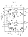
- FIG. 4 shows a circuit block diagram of a dual-band antenna duplexer. Blocks having similar functions to those in Fig. 2 are referenced correspondingly.
- An antenna duplexer 200 has a first transmitting/receiving circuit for a first mobile communication system (EGSM) and a second transmitting/receiving circuit for a second mobile communication system (PCN).
- the respective transmitting/receiving circuits are connected in parallel with an antenna terminal 3 through filters 21 and 22 respectively.
- the filters 21 and 22 are determined in accordance with frequency bands used in the respective communication systems.
- the filter 21 is a low pass filter which passes signals in the frequency band used in EGSM, that is, in the frequency band of not higher than 960 MHz.
- the filter 22 is a high pass filter which passes signals in the frequency band used in PCN, that is, in the frequency band of not lower than 1,710 MHz.
- the first transmitting/receiving circuit includes a receiving system constituted by a phase shift circuit 5-1, a matching circuit 6-1 and an SAW filter 24, and a transmitting system constituted by a phase shift circuit 5-2, matching circuits 6-2 and 6-3, and switching circuits 26, 27 and 29.
- the transmitting and receiving systems are connected in parallel with each other at a first parallel connection point 19. In such a parallel connection, it is necessary that, viewed from the parallel connection point, the impedance of the receiving system is made sufficiently high in the transmitting frequency band while the impedance of the transmitting system is made sufficiently high in the receiving frequency band so that signals can be prevented from leaking from one system into the other system.
- an EGSM reception signal outputted from the antenna terminal 3 is supplied to the receiving system through the low pass filter 21 and the first parallel connection point 19. Then, in order to restrain the leakage of the EGSM reception signal into the transmitting system, it is preferable that, viewed from the first parallel connection point 19, the absolute value of the reflection coefficient of the transmitting system including the switching circuits 26, 27 and 29 which are OFF is not less than 0.8 in the receiving frequency band f R (1).
- an EGSM transmission signal outputted from an EGSM transmitting terminal 32 is supplied to the antenna terminal 3 through the switching circuits 26, 27 and 29 which are tuned ON by a driving current 28 supplied from a bias terminal 30, the first parallel connection point 19 and the low pass filter 21. Then, in order to restrain the leakage of the EGSM transmission signal into the receiving system, it is preferable that, viewed from the first parallel connection point 19, the absolute value of the reflection coefficient of the receiving system including the SAW filter 24 is not less than 0.8 in the transmitting frequency band f T (1).
- Each of the matching circuits 6-2 and 6-3 in the transmitting system may have not only a function of impedance matching between the switching circuits but also a function as a low pass filter for eliminating second and third harmonics generated in the HPA.
- the driving current 28 outputted from the bias terminal 30 is grounded through the bias circuit 29, the switching element 26 and the feedback circuit 27.
- a capacity 23 is provided for preventing this bias current from leaking from the transmitting system into the antenna terminal 3. The absolute value of the reflection coefficient will be described later.
- the phase shift circuit 5-1 or 5-2 has a function of setting the optimum condition that the impedance of the transmitting or receiving system takes a maximum value in the receiving or transmitting frequency band. In this condition, the real part of the impedance is made maximum.
- a condition is achieved by a phase shift circuit, as well known in network theory.
- the phase shift circuit can be realized by a known circuit constituted by capacities, inductors, etc.
- Fig. 15 shows a relationship between the absolute value (
- ) of the reflection coefficient of the receiving (or transmitting) system and the loss (IL(dB)) in parallel connection when the impedance of the transmitting or receiving system is set to the optimum condition. Then, the loss in parallel connection IL(dB) is expressed by: IL(dB) -20log 10 (2 ⁇ (1+
- the SAW filter or switching circuits may have a function as the phase shift circuits 5 or the matching circuits 6. If these functions are achieved by the SAW filter or switching circuits, the circuits 5 and 6 can be omitted. Further, if the optimum condition of impedance is achieved by the SAW filter or switching circuits, and the matching circuits 6, the phase shift circuits 5 can be omitted.
- the second transmitting/receiving circuit includes a receiving system constituted by a phase shift circuit 5-1, a matching circuit 6-1 and an SAW filter 25, and a transmitting system constituted by a phase shift circuit 5-2, matching circuits 6-2 and 6-3, and switching circuits 26, 27 and 29.
- the transmitting and receiving systems are connected in parallel with each other at a second parallel connection point 20. Blocks having similar functions to those of the first transmitting/receiving circuit are referenced correspondingly.
- a PCN reception signal outputted from the antenna terminal 3 is supplied to the receiving system through the high pass filter 22 and the second parallel connection point 20. Then, in the same manner as in the first transmitting/receiving circuit, in order to restrain the leakage of the PCN reception signal into the transmitting system, it is preferable that, viewed from the second parallel connection point 20, the absolute value of the reflection coefficient of the transmitting system including the switching circuits 26, 27 and 29 which are OFF is not less than 0.8 in the receiving frequency band f R (2).
- a PCN transmission signal outputted from a PCN transmitting terminal 34 is supplied to the antenna terminal 3 through the switching circuits 26, 27 and 29 which are tuned ON by the driving current 28 supplied from a bias terminal 35, the second parallel connection point 20 and the high pass filter 22. Then, in the same manner as in the first transmitting/receiving circuit, in order to restrain the leakage of the PCN transmission signal into the receiving system, it is preferable that, viewed from the second parallel connection point 20, the absolute value of the reflection coefficient of the receiving system including the SAW filter 25 is not less than 0.8 in the transmitting frequency band f T (2).
- bias terminal 30 or 35 To which bias terminal 30 or 35 the bias current is supplied is controlled by a not-shown control portion in accordance with transmission of EGSM or PCN.
- the antenna duplexer shown in this embodiment can be miniaturized also from the point of view of mounting when the mounting is performed by using the multi-layer substrate shown in the first embodiment.
- the matching circuits, the phase shift circuits, the switching circuits, the bias circuits, etc. are constituted by lumped-constant circuit elements and mounted on the upper surface of the upper dielectric substrate.
- the SAW filters for EGSM and PCN are received in a space provided in the lower dielectric substrate.
- the mobile communication systems for providing service are not always limited to EGSM and PCN, but this embodiment is applicable to an antenna duplexer adapted to a combination of other mobile communication systems such as a W-CDMA system with a 2 GHz band and so on.
- the transmitting and receiving frequency bands f T (1) and f R (1) of EGSM are in a range of from 880 to 915 MHz and in a range of from 925 to 960 MHz respectively as shown in Fig. 1A.
- the transmitting and receiving frequency bands f T (2) and f R (2) of PCN are in a range of from 1,710 to 1,785 MHz and in a range of from 1,805 to 1,880 MHZ respectively as shown in Fig. 1B.
- the transmitting and receiving frequency bands f T (3) and f R (3) of PCS are in a range of from 1,850 to 1,910 MHz and in a range of from 1,930 to 1,990 MHz respectively as shown in Fig. 1C.
- the triple-band mobile radio terminal is adapted to a combination of mobile communication systems which include one 800 MHz band system and two other 1.5-2.0 GHz band systems, or two 800 MHz band systems and one other 1.5-2.0 GHz band system. Therefore, parts of circuits are shared between the two systems using neighboring frequency bands so that the circuit scale is reduced.
- the first mobile communication system is EGSM
- the second mobile communication system is PCN
- the third mobile communication system is PCS.
- the circuit configuration of the triple-band mobile radio terminal is also based on Fig. 16.
- three RF systems are required on the receiving system side, and oscillators of an off-set synthesizer and HPAs are required for three transmitting frequency bands on the transmitting system side.
- a basic configuration of the antenna duplexer is provided with a first transmitting/receiving circuit adapted to the 800 MHz band system (EGSM), and a second transmitting/receiving circuit adapted to the 1.5-2.0 GHz band systems (PCN and PCS).
- EGSM 800 MHz band system
- PCN and PCS 1.5-2.0 GHz band systems
- a first transmitting/receiving circuit a first transmitting system and a first receiving system are connected in parallel with each other in the same manner as in the second embodiment.
- a transmitting system is shared between PCN and PCS because PCN and PCS have transmitting frequency bands close to each other as shown in Figs. 1B and 1C.
- a second receiving system adapted to PCN and a third receiving system adapted to PCS are connected in parallel with each other. Further, the receiving systems connected in parallel and the transmitting system (second transmitting system) are connected in parallel.
- the impedance of the transmitting (receiving) system is made sufficiently high in the receiving (transmitting) frequency band.
- the impedance of the second (third) receiving system is made sufficiently high in the PCS (PCN) receiving frequency band.
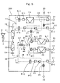
- FIG. 5 shows a circuit block diagram of a triple-band antenna duplexer. Blocks having similar functions to those in Figs. 2 and 4 are referenced correspondingly.
- An antenna duplexer 300 includes a first transmitting/receiving circuit for a first mobile communication system (EGSM) and a second transmitting/receiving circuit for second and third mobile communication systems (PCN and PCS). The respective transmitting/receiving circuits are connected in parallel with an antenna terminal 3 through filters 21 and 22 respectively.
- the filter 21 is a low pass filter which passes signals of the frequency band not higher than 960 MHz which is used in EGSM.
- the filter 22 is a high pass filter which passes signals of the frequency band not lower than 1,710 MHz which is used in PCN and PCS. Description is omitted as to the circuit configuration and operation of the first transmitting/receiving circuit because they are similar to those which were described in the second embodiment.
- the circuit includes a second receiving system constituted by phase shift circuits 5-1, matching circuits 6-1, and SAW filters 25 and 39, and a second transmitting system constituted by a phase shift circuit 5-2, matching circuits 6-2 and 6-3, and switching circuits 26 and 29.
- the second receiving and transmitting systems are connected in parallel with each other at a parallel connection point (referred to as "third parallel connection point") 36.
- the receiving system is provided with second and third receiving systems each constituted by a phase shift circuit, a matching circuit and an SAW filter so as to be adapted to PCN and PCS.
- the second and third receiving systems are connected in parallel with each other at a parallel connection point (referred to as "fourth parallel connection point) 38.
- a PCN reception signal outputted from the antenna terminal 3 is supplied to the receiving system through the high pass filter 22 and the third parallel connection point 36. Further, the signal is supplied to the second receiving system adapted to PCN through the fourth parallel connection point 38. Then, in order to restrain the leakage of the PCN reception signal into the third receiving system adapted to PCS, it is preferable that, viewed from the fourth parallel connection point 38, the absolute value of the reflection coefficient of the third receiving system including the SAW filter 39 is not less than 0.8 in the receiving frequency band f R (2).
- a PCS reception signal is supplied to the receiving system in the same manner as in the PCN signal, and the PCS reception signal is supplied to the third receiving system adapted to PCS through the fourth parallel connection point 38. Then, in order to restrain the leakage of the PCS reception signal into the second receiving system adapted to PCN, it is preferable that, viewed from the fourth parallel connection point 38, the absolute value of the reflection coefficient of the second receiving system including the SAW filter 25 is not less than 0.8 in the receiving frequency band f R (3).
- the absolute value of the reflection coefficient of the second transmitting system including the switching circuits 26 and 29 which are OFF is not less than 0.8 in the receiving frequency bands f R (2) and f R (3).
- a PCN or PCS transmission signal outputted from a transmitting terminal 41 is supplied to the antenna terminal 3 through the switching circuits 26 and 29 which are tuned ON by a driving current 28 supplied from a bias terminal 42, the third parallel connection point 36 and the high pass filter 22. Then, in order to restrain the leakage of the PCN or PCS transmission signal to the receiving system, it is preferable that, viewed from the third parallel connection point 36, the absolute value of the reflection coefficient of the receiving system including the SAW filters 25 and 39 is not less than 0.8 in the transmitting frequency bands f T (2) and f T (3).
- the driving current 28 is outputted from the bias terminal 42 and grounded through the bias circuit 29, the switching element 26, a phase shift circuit 37 and the switching element 26'.
- This phase shift circuit 37 has the same function as a quarter-wave line so as to restrain the leakage of the PCN or PCS transmission signal into the receiving system.
- the receiving system is OFF when the switching elements 26 and 26' are ON so that the driving current 28 flows into the phase shift circuit 37.
- the receiving system is ON when the switching elements 26 and 26' are OFF so that the driving current 28 does not flow into the phase shift circuit 37.
- the phase shift circuit 37 is designed so that the impedance of the receiving system is made maximum viewed from the third parallel connection point 36 when the driving current 28 is flowing into the phase shift circuit 37, and the impedance of the receiving system is made minimum viewed from the third parallel connection point 36 when the driving current 28 is not flowing into the phase shift circuit 37.
- the phase shift circuit 37 may be formed by a known circuit configuration with capacities, inductors, etc.
- the parallel connections between the second transmitting system and the receiving system and between the second and third receiving systems may be replaced by the switching of switching elements.
- the absolute value of the reflection coefficient of each of the transmitting and receiving systems is ensured to be not less than 0.8.
- the frequency band is narrower, it is easier to keep a large absolute value of a reflection coefficient.
- a frequency distance between min(the lowest frequency of f T (2), the lowest frequency of f T (3)) and max(the highest frequency of f T (2), the highest frequency of f T (3)) and a frequency distance between min(the lowest frequency of f R (2), the lowest frequency of f R (3)) and max(the highest frequency of f R (2), the highest frequency of f R (3)) are as narrow as possible.
- the receiving frequency bands of the two systems do not overlap with each other.
- a triple-band mobile radio terminal adapted to one system using a frequency band near an 800 MHz band and two systems using frequency bands in a 1.5-2.0 GHz band.
- similar configuration can be applied to a triple-band mobile radio terminal adapted to two systems using frequency bands near an 800 MHz band and one system using a frequency band in a 1.5-2.0 GHz band.
- a transmitting/receiving circuit corresponding to the second transmitting/receiving circuit described above is connected to a low pass filter connected to the antenna terminal 3
- a transmitting/receiving circuit corresponding to the first transmitting/receiving circuit described above is connected to a high pass filter connected to the antenna terminal 3.
- the antenna duplexer shown in this embodiment can be miniaturized also from the point of view of mounting when the mounting is performed by using the multi-layer substrate shown in the first embodiment.
- the matching circuits, the phase shift circuits, the switching circuits, the bias circuits, etc. are constituted by lumped-constant circuit elements and mounted on the upper surface of the upper dielectric substrate.
- the SAW filters for EGSM, PCN and PCS are received in a space on the lower dielectric substrate.
- the mobile communication systems for providing service are not always limited to EGSM, PCN and PCS, but this embodiment is applicable to an antenna duplexer adapted to a predetermined combination of other mobile communications.
- an antenna duplexer can be miniaturized so that a dual-band/triple-band mobile radio terminal small in size and light in weight can be realized.
Landscapes
- Physics & Mathematics (AREA)
- Acoustics & Sound (AREA)
- Surface Acoustic Wave Elements And Circuit Networks Thereof (AREA)
- Transceivers (AREA)
- Support Of Aerials (AREA)
- Variable-Direction Aerials And Aerial Arrays (AREA)
Applications Claiming Priority (2)
| Application Number | Priority Date | Filing Date | Title |
|---|---|---|---|
| JP36407498A JP3484090B2 (ja) | 1998-12-22 | 1998-12-22 | スイッチ型アンテナ共用器および移動無線端末 |
| JP36407498 | 1998-12-22 |
Publications (2)
| Publication Number | Publication Date |
|---|---|
| EP1014592A2 true EP1014592A2 (de) | 2000-06-28 |
| EP1014592A3 EP1014592A3 (de) | 2004-04-21 |
Family
ID=18480912
Family Applications (1)
| Application Number | Title | Priority Date | Filing Date |
|---|---|---|---|
| EP99124880A Withdrawn EP1014592A3 (de) | 1998-12-22 | 1999-12-16 | Mobilfunkendgerät und Oberflächewellenantenneduplexer |
Country Status (3)
| Country | Link |
|---|---|
| US (1) | US6766149B1 (de) |
| EP (1) | EP1014592A3 (de) |
| JP (1) | JP3484090B2 (de) |
Cited By (18)
| Publication number | Priority date | Publication date | Assignee | Title |
|---|---|---|---|---|
| FR2812512A1 (fr) * | 2000-07-27 | 2002-02-01 | Murata Manufacturing Co | Module haute frequence et appareil de communication mobile l'utilisant |
| US6380823B1 (en) * | 1999-06-04 | 2002-04-30 | Fujitsu Limited | Antenna duplexer with receiving, transmitting, and antenna terminal groups separated planarly |
| WO2002007337A3 (en) * | 2000-07-14 | 2002-06-27 | Ericsson Telefon Ab L M | Frequency multiplexer |
| EP1223634A2 (de) | 2000-12-26 | 2002-07-17 | Matsushita Electric Industrial Co., Ltd. | Hochfrequenzschalter, laminierter Hochfrequenzschalter, Hochfrequenz-Funkeinheit und Hochfrequenz-Schaltverfahren |
| US6456172B1 (en) * | 1999-10-21 | 2002-09-24 | Matsushita Electric Industrial Co., Ltd. | Multilayered ceramic RF device |
| US6563396B2 (en) * | 1999-09-28 | 2003-05-13 | Murata Manufacturing Co., Ltd. | Composite high frequency component and mobile communication apparatus incorporating the same |
| US6570469B2 (en) * | 2000-06-27 | 2003-05-27 | Matsushita Electric Industrial Co., Ltd. | Multilayer ceramic device including two ceramic layers with multilayer circuit patterns that can support semiconductor and saw chips |
| EP1237290A3 (de) * | 2001-02-27 | 2003-12-10 | Matsushita Electric Industrial Co., Ltd. | Antennenduplexer und mobile Kommunikationseinrichtung, die diesen benutzt |
| EP1298756A3 (de) * | 2001-10-01 | 2004-01-02 | Matsushita Electric Industrial Co., Ltd. | Zusammengestelltes Filter, Antennenweiche und Kommunikationsgerät |
| EP1083672A4 (de) * | 1999-03-18 | 2004-06-23 | Hitachi Metals Ltd | Hochfrequenzschaltermodul |
| US7003312B2 (en) * | 1999-12-28 | 2006-02-21 | Hitachi Metals, Ltd. | High-frequency switch circuit, high-frequency switch module and wireless communication device |
| US7253702B2 (en) * | 2000-11-01 | 2007-08-07 | Hitachi Metals, Ltd. | High-frequency switch module |
| WO2008135597A1 (de) * | 2007-05-08 | 2008-11-13 | Epcos Ag | Elektrisches bauelement mit einer frontend-schaltung |
| EP1233528A4 (de) * | 2000-10-06 | 2009-07-22 | Panasonic Corp | Zusammengesetztes hochfrequenz-schaltmodul |
| CN1951006B (zh) * | 2004-04-30 | 2010-05-05 | 诺基亚公司 | 在多频段通信中使用的方法、收发机和通信设备 |
| EP1695447A4 (de) * | 2003-10-17 | 2013-03-20 | Nokia Corp | Frontend-anordnung für mehrband-multimodus-kommunikations-engines |
| EP2728759A1 (de) * | 2012-10-30 | 2014-05-07 | Panasonic Corporation | Antennenanpassungsschaltung für drahtlose Kommunikationsvorrichtung |
| CN112751191A (zh) * | 2019-10-29 | 2021-05-04 | Oppo广东移动通信有限公司 | 一种天线模组和移动终端 |
Families Citing this family (38)
| Publication number | Priority date | Publication date | Assignee | Title |
|---|---|---|---|---|
| US7035602B2 (en) | 1999-12-14 | 2006-04-25 | Matsushita Electric Industrial Co., Ltd. | High-frequency composite switch component |
| JP3480445B2 (ja) | 2001-01-10 | 2003-12-22 | 株式会社村田製作所 | 弾性表面波装置 |
| JP2007174713A (ja) * | 2001-03-30 | 2007-07-05 | Hitachi Media Electoronics Co Ltd | 高周波フィルタ、高周波回路、アンテナ共用器及び無線端末 |
| US6995630B2 (en) * | 2001-10-24 | 2006-02-07 | Matsushita Electric Industrial Co., Ltd. | High-frequency compound switch module and communication terminal using it |
| US7277403B2 (en) * | 2001-12-13 | 2007-10-02 | Avago Technologies Wireless Ip (Singapore) Pte Ltd | Duplexer with a differential receiver port implemented using acoustic resonator elements |
| JP3833569B2 (ja) | 2001-12-21 | 2006-10-11 | 富士通メディアデバイス株式会社 | 分波器及びこれを用いた電子装置 |
| JP2003264348A (ja) * | 2002-03-07 | 2003-09-19 | Sony Corp | 高周波モジュール |
| US7936714B1 (en) | 2002-03-11 | 2011-05-03 | Netgear, Inc. | Spectrum allocation system and method for multi-band wireless RF data communications |
| GB2387508B (en) | 2002-04-12 | 2005-06-29 | Nec Technologies | Mobile radio communications device and method of operation |
| EP1502364A4 (de) | 2002-04-22 | 2010-03-31 | Ipr Licensing Inc | Funksender/-empfänger mit mehreren eingängen und mehreren ausgängen |
| KR100574533B1 (ko) * | 2002-07-30 | 2006-04-27 | 엘지이노텍 주식회사 | Fem 칩 제조방법 |
| US6973330B2 (en) * | 2002-10-04 | 2005-12-06 | Sony Corporation | Optimized two-sided wireless modem card component placement |
| JP2004147045A (ja) * | 2002-10-24 | 2004-05-20 | Matsushita Electric Ind Co Ltd | 高周波スイッチ |
| US7373171B2 (en) * | 2003-02-14 | 2008-05-13 | Tdk Corporation | Front end module |
| JP2005117139A (ja) * | 2003-10-03 | 2005-04-28 | Mitsubishi Electric Corp | マイクロ波モジュール、及びこれを用いたアレーアンテナ装置 |
| CN100530958C (zh) * | 2003-10-16 | 2009-08-19 | 京瓷株式会社 | 复合型分波电路、用其的芯片零件、高频模块及无线通信设备 |
| JP4418250B2 (ja) * | 2004-02-05 | 2010-02-17 | 株式会社ルネサステクノロジ | 高周波回路モジュール |
| US7187945B2 (en) * | 2004-04-30 | 2007-03-06 | Nokia Corporation | Versatile antenna switch architecture |
| US20070030095A1 (en) * | 2005-08-05 | 2007-02-08 | Mitsutaka Hikita | Antenna duplexer and wireless terminal using the same |
| KR20070106091A (ko) * | 2006-04-28 | 2007-11-01 | 삼성전자주식회사 | 코드분할 다중접속 통신시스템과 일본식 코드분할 다중접속통신시스템 공유장치 |
| WO2008013170A1 (en) * | 2006-07-25 | 2008-01-31 | Murata Manufacturing Co., Ltd. | High frequency module and communication apparatus using same |
| JP5262413B2 (ja) * | 2008-08-12 | 2013-08-14 | 株式会社村田製作所 | マルチバンドデュプレクサモジュール |
| US20120139813A1 (en) * | 2009-06-18 | 2012-06-07 | Jaume Anguera | Wireless device providing operability for broadcast standards and method enabling such operability |
| JP5377243B2 (ja) * | 2009-11-25 | 2013-12-25 | 京セラ株式会社 | 圧電電子部品 |
| JP4858733B1 (ja) * | 2010-10-06 | 2012-01-18 | 横浜ゴム株式会社 | 送信装置 |
| US8892159B2 (en) * | 2011-05-12 | 2014-11-18 | St-Ericsson Sa | Multi-standard transceiver architecture with common balun and mixer |
| JP5777975B2 (ja) | 2011-08-22 | 2015-09-16 | 太陽誘電株式会社 | 通信モジュール |
| US9058455B2 (en) * | 2012-01-20 | 2015-06-16 | International Business Machines Corporation | Backside integration of RF filters for RF front end modules and design structure |
| KR101915526B1 (ko) * | 2012-04-17 | 2018-11-06 | 삼성전자 주식회사 | 휴대 단말기의 안테나 장치 |
| JP6105358B2 (ja) * | 2013-04-02 | 2017-03-29 | 太陽誘電株式会社 | 回路基板 |
| WO2017221953A1 (ja) | 2016-06-21 | 2017-12-28 | 株式会社村田製作所 | 弾性波デバイス |
| US9998097B2 (en) * | 2016-07-15 | 2018-06-12 | Murata Manufacturing Co., Ltd. | Radio-frequency front-end circuit and communication device |
| CA3092066A1 (en) * | 2018-02-22 | 2019-08-29 | Dexcom, Inc. | Sensor interposers employing castellated through-vias |
| KR102438877B1 (ko) * | 2018-06-20 | 2022-09-01 | 가부시키가이샤 무라타 세이사쿠쇼 | 고주파 모듈 및 통신 장치 |
| US11658688B2 (en) * | 2019-05-01 | 2023-05-23 | Skyworks Solutions, Inc. | Multiplexer with bulk acoustic wave filter and multilayer piezoelectric substrate filter |
| JP2021145282A (ja) * | 2020-03-13 | 2021-09-24 | 株式会社村田製作所 | 高周波モジュールおよび通信装置 |
| JP2021158556A (ja) * | 2020-03-27 | 2021-10-07 | 株式会社村田製作所 | 高周波モジュールおよび通信装置 |
| JP2021158554A (ja) * | 2020-03-27 | 2021-10-07 | 株式会社村田製作所 | 高周波モジュールおよび通信装置 |
Family Cites Families (11)
| Publication number | Priority date | Publication date | Assignee | Title |
|---|---|---|---|---|
| DE69307412T2 (de) * | 1992-07-08 | 1997-06-12 | Matsushita Electric Ind Co Ltd | Antennenumschaltanordnung zum Selektiven Verbinden einer Antenne mit einem Sender oder einem Empfänger |
| US5483678A (en) * | 1992-09-28 | 1996-01-09 | Fujitsu Limited | Internal microstrip antenna for radio telephones |
| FI97086C (fi) * | 1994-02-09 | 1996-10-10 | Lk Products Oy | Järjestely lähetyksen ja vastaanoton erottamiseksi |
| JPH07226607A (ja) * | 1994-02-10 | 1995-08-22 | Hitachi Ltd | 分波器、分波器モジュールおよび無線通信装置 |
| JP3139327B2 (ja) * | 1995-05-31 | 2001-02-26 | 株式会社村田製作所 | 高周波複合部品 |
| US5786738A (en) * | 1995-05-31 | 1998-07-28 | Fujitsu Limited | Surface acoustic wave filter duplexer comprising a multi-layer package and phase matching patterns |
| KR100213372B1 (ko) * | 1996-05-10 | 1999-08-02 | 이형도 | 모노리틱 쏘 듀플렉서 |
| JPH1032521A (ja) * | 1996-07-17 | 1998-02-03 | Murata Mfg Co Ltd | デュプレクサ |
| DE69722168T2 (de) * | 1997-02-12 | 2003-12-18 | Oki Electric Ind Co Ltd | Akustische Oberflächenwellenfilter mit erzeugten Dämpfungspolen durch Impedanzschaltungen |
| US6169733B1 (en) * | 1997-05-12 | 2001-01-02 | Northern Telecom Limited | Multiple mode capable radio receiver device |
| US6535166B1 (en) * | 2001-01-08 | 2003-03-18 | Ericsson Inc. | Capacitively coupled plated antenna |
-
1998
- 1998-12-22 JP JP36407498A patent/JP3484090B2/ja not_active Expired - Fee Related
-
1999
- 1999-12-16 EP EP99124880A patent/EP1014592A3/de not_active Withdrawn
- 1999-12-22 US US09/469,369 patent/US6766149B1/en not_active Expired - Fee Related
Cited By (40)
| Publication number | Priority date | Publication date | Assignee | Title |
|---|---|---|---|---|
| EP1801990A1 (de) * | 1999-03-18 | 2007-06-27 | Hitachi Metals, Ltd. | Hochfrequenzschalter |
| US7171234B2 (en) | 1999-03-18 | 2007-01-30 | Marino-Forum21 | High-frequency switch circuit |
| US7130655B2 (en) | 1999-03-18 | 2006-10-31 | Marino-Forum 21 | High-frequency switch circuit |
| US6987984B1 (en) | 1999-03-18 | 2006-01-17 | Hitachi Metals, Ltd. | High-frequency switch module |
| EP1083672A4 (de) * | 1999-03-18 | 2004-06-23 | Hitachi Metals Ltd | Hochfrequenzschaltermodul |
| US6380823B1 (en) * | 1999-06-04 | 2002-04-30 | Fujitsu Limited | Antenna duplexer with receiving, transmitting, and antenna terminal groups separated planarly |
| EP1089449A3 (de) * | 1999-09-28 | 2004-02-04 | Murata Manufacturing Co., Ltd. | Diplexerschaltung eines mobilen Nachrichtengerätes |
| US6563396B2 (en) * | 1999-09-28 | 2003-05-13 | Murata Manufacturing Co., Ltd. | Composite high frequency component and mobile communication apparatus incorporating the same |
| US6456172B1 (en) * | 1999-10-21 | 2002-09-24 | Matsushita Electric Industrial Co., Ltd. | Multilayered ceramic RF device |
| US7471962B2 (en) | 1999-12-28 | 2008-12-30 | Hitachi Metals, Ltd. | High-frequency switch circuit, high-frequency switch module and wireless communications device comprising it |
| US7003312B2 (en) * | 1999-12-28 | 2006-02-21 | Hitachi Metals, Ltd. | High-frequency switch circuit, high-frequency switch module and wireless communication device |
| US6570469B2 (en) * | 2000-06-27 | 2003-05-27 | Matsushita Electric Industrial Co., Ltd. | Multilayer ceramic device including two ceramic layers with multilayer circuit patterns that can support semiconductor and saw chips |
| US6784765B2 (en) | 2000-06-27 | 2004-08-31 | Matsushita Electric Industrial Co., Ltd. | Multilayer ceramic device |
| WO2002007337A3 (en) * | 2000-07-14 | 2002-06-27 | Ericsson Telefon Ab L M | Frequency multiplexer |
| US6950410B1 (en) | 2000-07-14 | 2005-09-27 | Telefonaktiebolaget Lm Ericsson (Publ) | Frequency multiplexer |
| US6788958B2 (en) | 2000-07-27 | 2004-09-07 | Murata Manufacturing Co., Ltd. | High-frequency module and mobile communication apparatus using the same |
| FR2812512A1 (fr) * | 2000-07-27 | 2002-02-01 | Murata Manufacturing Co | Module haute frequence et appareil de communication mobile l'utilisant |
| US7398103B2 (en) | 2000-07-27 | 2008-07-08 | Murata Manufacturing Co., Ltd. | High-frequency module and mobile communication apparatus using the same |
| DE10136337B4 (de) * | 2000-07-27 | 2005-04-28 | Murata Manufacturing Co | Hochfrequenzmodul und Verwendung desselben in einer Mobilen Kommunikationsvorrichtung |
| GB2369013A (en) * | 2000-07-27 | 2002-05-15 | Murata Manufacturing Co | High frequency module for a triple-band mobile telephone |
| GB2369013B (en) * | 2000-07-27 | 2003-04-23 | Murata Manufacturing Co | High-frequency module and mobile communication apparatus using the same |
| EP1233528A4 (de) * | 2000-10-06 | 2009-07-22 | Panasonic Corp | Zusammengesetztes hochfrequenz-schaltmodul |
| EP1333588A4 (de) * | 2000-11-01 | 2009-07-22 | Hitachi Metals Ltd | Hochfrequenz-schaltmodul |
| US7253702B2 (en) * | 2000-11-01 | 2007-08-07 | Hitachi Metals, Ltd. | High-frequency switch module |
| EP1223634A2 (de) | 2000-12-26 | 2002-07-17 | Matsushita Electric Industrial Co., Ltd. | Hochfrequenzschalter, laminierter Hochfrequenzschalter, Hochfrequenz-Funkeinheit und Hochfrequenz-Schaltverfahren |
| US7023296B2 (en) | 2000-12-26 | 2006-04-04 | Matsushita Electric Industrial Co., Ltd. | High-frequency switch, laminated high-frequency switch, high-frequency radio unit, and high-frequency switching method |
| US6867662B2 (en) | 2000-12-26 | 2005-03-15 | Matsushita Electric Industrial Co., Ltd. | High-frequency switch, laminated high-frequency switch, high-frequency radio unit, and high-frequency switching method |
| US7038557B2 (en) | 2001-02-27 | 2006-05-02 | Matsushita Electric Industrial Co., Ltd. | Antenna duplexer and mobile communication device using the same |
| EP1508974A3 (de) * | 2001-02-27 | 2005-09-14 | Matsushita Electric Industrial Co., Ltd. | Antennenweiche und deren Verwendung in einem mobilen Kommunikationsgerät |
| EP1237290A3 (de) * | 2001-02-27 | 2003-12-10 | Matsushita Electric Industrial Co., Ltd. | Antennenduplexer und mobile Kommunikationseinrichtung, die diesen benutzt |
| EP1298756A3 (de) * | 2001-10-01 | 2004-01-02 | Matsushita Electric Industrial Co., Ltd. | Zusammengestelltes Filter, Antennenweiche und Kommunikationsgerät |
| US6809611B2 (en) | 2001-10-01 | 2004-10-26 | Matsushita Electric Industrial Co., Ltd. | Composite filter, antenna duplexer, and communication apparatus |
| EP1695447A4 (de) * | 2003-10-17 | 2013-03-20 | Nokia Corp | Frontend-anordnung für mehrband-multimodus-kommunikations-engines |
| CN1951006B (zh) * | 2004-04-30 | 2010-05-05 | 诺基亚公司 | 在多频段通信中使用的方法、收发机和通信设备 |
| WO2008135597A1 (de) * | 2007-05-08 | 2008-11-13 | Epcos Ag | Elektrisches bauelement mit einer frontend-schaltung |
| US8620244B2 (en) | 2007-05-08 | 2013-12-31 | Epcos Ag | Electrical component with a front-end circuit |
| EP2728759A1 (de) * | 2012-10-30 | 2014-05-07 | Panasonic Corporation | Antennenanpassungsschaltung für drahtlose Kommunikationsvorrichtung |
| US8923783B2 (en) | 2012-10-30 | 2014-12-30 | Panasonic Corporation | Transmit and receive transmission circuits coupled to a common antenna for a wireless communication device |
| CN112751191A (zh) * | 2019-10-29 | 2021-05-04 | Oppo广东移动通信有限公司 | 一种天线模组和移动终端 |
| CN112751191B (zh) * | 2019-10-29 | 2023-07-21 | Oppo广东移动通信有限公司 | 一种天线模组和移动终端 |
Also Published As
| Publication number | Publication date |
|---|---|
| JP2000188522A (ja) | 2000-07-04 |
| US6766149B1 (en) | 2004-07-20 |
| JP3484090B2 (ja) | 2004-01-06 |
| EP1014592A3 (de) | 2004-04-21 |
Similar Documents
| Publication | Publication Date | Title |
|---|---|---|
| US6766149B1 (en) | Mobile radio terminal and surface acoustic wave antenna duplexer | |
| US7053731B2 (en) | Duplexer using surface acoustic wave filters | |
| US7373171B2 (en) | Front end module | |
| EP1079534B1 (de) | Bandgeschalteten Oberflächenwellen-Antenneduplexer und Mobilfunkendgerät | |
| US7941103B2 (en) | Duplexer | |
| Lin et al. | Design of an LTCC tri-band transceiver module for GPRS mobile applications | |
| CN1881810B (zh) | 多模式高频电路 | |
| US7050769B2 (en) | Electronic apparatus and design method | |
| Meier et al. | Miniaturization and advanced functionalities of SAW devices | |
| US6919778B2 (en) | Duplexer with an impedance matching circuit and an electronic device using the same | |
| US7684764B2 (en) | Duplexer using surface acoustic wave filters and electronic device equipped with the same | |
| JP4221205B2 (ja) | ダイプレクサ並びにそれを用いた高周波スイッチ | |
| CN100481725C (zh) | 天线双工器和电子设备 | |
| JPH08125413A (ja) | 平衡不平衡変換回路 | |
| US6996384B2 (en) | Receiver and radio communication terminal using the same | |
| US20040240420A1 (en) | Front end module and high-frequency functional module | |
| JP3752231B2 (ja) | フロントエンドモジュール | |
| JP3752232B2 (ja) | フロントエンドモジュール | |
| JP4446922B2 (ja) | フィルタおよび分波器 | |
| JP3851184B2 (ja) | フロントエンドモジュール | |
| JP3760084B2 (ja) | アンテナ共用器 | |
| JP3830369B2 (ja) | 高周波回路、複合高周波部品及びそれを用いた通信装置 | |
| JP3959268B2 (ja) | 高周波回路、複合高周波部品及びそれを用いた通信装置 | |
| JP2002300006A (ja) | 高周波部品及びアンテナ共用器 |
Legal Events
| Date | Code | Title | Description |
|---|---|---|---|
| PUAI | Public reference made under article 153(3) epc to a published international application that has entered the european phase |
Free format text: ORIGINAL CODE: 0009012 |
|
| AK | Designated contracting states |
Kind code of ref document: A2 Designated state(s): AT BE CH CY DE DK ES FI FR GB GR IE IT LI LU MC NL PT SE |
|
| AX | Request for extension of the european patent |
Free format text: AL;LT;LV;MK;RO;SI |
|
| 17P | Request for examination filed |
Effective date: 20031124 |
|
| PUAL | Search report despatched |
Free format text: ORIGINAL CODE: 0009013 |
|
| AK | Designated contracting states |
Kind code of ref document: A3 Designated state(s): AT BE CH CY DE DK ES FI FR GB GR IE IT LI LU MC NL PT SE |
|
| AX | Request for extension of the european patent |
Extension state: AL LT LV MK RO SI |
|
| AKX | Designation fees paid |
Designated state(s): DE FR GB |
|
| 17Q | First examination report despatched |
Effective date: 20070831 |
|
| STAA | Information on the status of an ep patent application or granted ep patent |
Free format text: STATUS: THE APPLICATION IS DEEMED TO BE WITHDRAWN |
|
| 18D | Application deemed to be withdrawn |
Effective date: 20121201 |