EP1223634A2 - Hochfrequenzschalter, laminierter Hochfrequenzschalter, Hochfrequenz-Funkeinheit und Hochfrequenz-Schaltverfahren - Google Patents
Hochfrequenzschalter, laminierter Hochfrequenzschalter, Hochfrequenz-Funkeinheit und Hochfrequenz-Schaltverfahren Download PDFInfo
- Publication number
- EP1223634A2 EP1223634A2 EP01130694A EP01130694A EP1223634A2 EP 1223634 A2 EP1223634 A2 EP 1223634A2 EP 01130694 A EP01130694 A EP 01130694A EP 01130694 A EP01130694 A EP 01130694A EP 1223634 A2 EP1223634 A2 EP 1223634A2
- Authority
- EP
- European Patent Office
- Prior art keywords
- circuit
- terminal
- receiving
- transmission
- signal transfer
- Prior art date
- Legal status (The legal status is an assumption and is not a legal conclusion. Google has not performed a legal analysis and makes no representation as to the accuracy of the status listed.)
- Withdrawn
Links
Images

Classifications
-
- H—ELECTRICITY
- H01—ELECTRIC ELEMENTS
- H01P—WAVEGUIDES; RESONATORS, LINES, OR OTHER DEVICES OF THE WAVEGUIDE TYPE
- H01P1/00—Auxiliary devices
- H01P1/10—Auxiliary devices for switching or interrupting
- H01P1/15—Auxiliary devices for switching or interrupting by semiconductor devices
Definitions
- the present invention relates to a high-frequency switch used to switch between transmission and reception signals in a three- or four-frequency band of a portable telephone, a laminated high-frequency switch, a high-frequency radio unit, and a high-frequency switching method.
- a conventional high-frequency switch for switching between transmission and reception signals in a three-frequency band specifically EGSM transmission and reception signals in 900-MHz band, DCS transmission and reception signals in 1, 800-MHz band, and PCS transmission and reception signals in 1,900-MHz band is described below with reference to the accompanying drawings.
- FIG. 10 shows a conventional high-frequency switch for switching between frequency-band signals.
- the conventional high-frequency switch is constituted by a first transmission-reception switching circuit 11, a second transmission-reception switching circuit 12, a diplexer 13, and an auxiliary switching circuit 14.
- a diplexer 13 is described in accordance with FIG. 10.
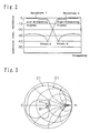
- a low-pass filter for passing a low-frequency signal like a waveform 1 shown in FIG. 2 is formed by a fifth strip line L5, a sixth strip line L6, and a seventh capacitor C7 of the diplexer 13 and an attenuation pole A is formed by the fact that the sixth strip line L6 and the seventh capacitor C7 constitute a series circuit which is connected to the earth side.
- an attenuation pole B is formed by the fact that the eleventh strip line L11 and fourteenth capacitor C14 constitute a series circuit which is connected to the earth side.
- the high-pass filter side when transmitting or receiving a low-frequency signal (EGSM signal in 900-MHz band), the high-pass filter side preferably obtains isolation against a low-frequency signal from a point C by the attenuation pole B and therefore, no signal leaks to the high-pass filter side. Moreover, when transmitting or receiving a high-frequency signal, the low-pass filter side obtains isolation from the point C against a high frequency by the attenuation pole A and therefore, no signal leaks to the low-pass filter side. That is, the diplexer 13 has a function for branching a low-frequency signal and a high-frequency signal.
- the first transmission-reception switching circuit 11 is described below.
- a first diode P1 and a second diode P2 are turned on.
- a first capacitor C1 a fourth capacitor C4, a sixth capacitor C6, and the thirteenth capacitor C13 prevent DC components, no DC current flows through each terminal.
- the impedance of a third strip line L3 infinitely increases when the second diode P2 is connected to the earth side, a signal sent from a transmitting-circuit terminal Tx1 is not transferred to a receiving-circuit terminal Rx1.
- the inductance component of the second diode P2 resonates with a fifth capacitor C5
- the second transmission-reception switching circuit 12 is a circuit for transmitting or receiving frequency signals having a frequency higher than the case of the first transmission-reception switching circuit 11 (DCS signal in 1,800-MHz band and PCS signal in 1,900-MHz band) .
- the circuit configuration of the second transmission-reception switching circuit 12 is completely the same as that of first transmission-reception switching circuit 11. Therefore, when transmitting a high frequency, by applying a positive voltage to a control terminal Vc2, a transmission signal is transferred from the transmitting-circuit terminal Tx2 to the antenna terminal ANT through the high-pass filter of the diplexer 13.
- When receiving a high-frequency signal by applying no positive voltage to the control terminal Vc2, it is possible to transfer a reception signal from the antenna terminal ANT to the receiving-circuit terminal Rx2 through the high-pass filter of the diplexer 13.
- An auxiliary switching circuit 14 is a circuit for transferring a high-frequency reception signal input from the receiving-circuit terminal Rx2 of the second transmission-reception switching circuit 12 to the point D of the auxiliary switching circuit 14 by further switching the signal to receiving-circuit terminals Rx3 (PCS receiving terminal) and Rx4 (DCS receiving terminal) in two frequency bands different from each other.
- the configuration of the auxiliary switching circuit 14 is basically the same as those of the first transmission-reception switching circuit 11 and second transmission-reception switching circuit 12. Therefore , by applying a positive voltage to a control terminal Vc3, a reception signal is transferred from the receiving-circuit terminal Rx2 of the second transmission-reception switching circuit 12 to the third receiving-circuit terminal Rx3 via the point D of the auxiliary switching circuit 14.
- the reception signal is transferred from the receiving-circuit terminal Rx2 of the second transmission-reception switching circuit 12 to the fourth receiving-circuit terminal Rx4 via the point D of the auxiliary switching circuit 14.
- the high-frequency reception signal is transferred to the fourth receiving-circuit terminal Rx4 via the high-pass filter of the diplexer 13, the point B of the second transmission-reception switching circuit 12, and the point D of the auxiliary switching circuit 14.
- a conventional high-frequency switch thus switches between transmission and reception signals in three types of frequency bands.
- the present invention is made to solve the above conventional problems and its object is to provide a high-frequency switch, a laminated high-frequency switch, and a high-frequency radio unit for reducing the number of components to be mounted on the surface of a laminated substrate for the high-frequency switch.
- the 1st invention of the present invention is a high-frequency switch comprising:
- the 2nd invention of the present invention is the high-frequency switch according to 1st invention, wherein the first diplexer has a low-pass filter disposed between the antenna terminal and the first transmission-reception switching circuit and a high-pass filter disposed between the antenna terminal and the second transmission-reception switching circuit.
- the 3rd invention of the present invention is the high-frequency switch according to 2nd invention, wherein the first transmission-reception switching circuit has a first diode having an anode connected to the first transmitting-circuit terminal and a cathode connected to the low-pass, filter, a first strip line connected at one end to the anode of the first diode and grounded at the other end through a first capacitor and connected to a first control terminal, a second diode having an anode connected to the first receiving-circuit terminal and a cathode grounded through a parallel circuit constituted by a second capacitor and a second strip line, and a third strip line connected at one end to the anode of the second diode and connected at the other end to the low-pass filter; the second transmission-reception switching circuit has a third diode having an anode connected to the second transmitting-circuit terminal and a cathode connected to the high-pass filter, a fourth strip line connected at one end to the anode of the third dio
- the 4th invention of the present invention is the high-frequency switch according to 3rd invention, further comprising:
- the 5th invention of the present invention is the high-frequency switch according to 3rd invention, further comprising:
- the 6th invention of the present invention is the high-frequency switch according to 3rd invention, wherein the phase-shifting circuit has a seventh strip line connected at one end to the second receiving-circuit terminal and connected at the other end to the first surface-acoustic-wave filter, a fifth capacitor connected at one end to the second receiving-circuit terminal and grounded at the other end through a first inductor, and a sixth capacitor grounded at one end through the first inductor and connected to the fifth capacitor and connected at the other end to the second surface-acoustic-wave filter.
- the 7th invention of the present invention the high-frequency switch according to 3rd invention, wherein the phase-shifting circuit has a second inductor grounded at one end through a seventh capacitor and connected to the second receiving-circuit terminal and connected at the other end to the first surface-acoustic-wave filter, an eighth capacitor connected at one end to the second receiving-circuit terminal and grounded at the other end through a third inductor, and a ninth capacitor grounded at one end through the third inductor and connected to the eighth capacitor and connected at the other end to the second surface-acoustic-wave filter.
- the 8th invention of the present invention is a high-frequency switch comprising:
- the 9th invention of the present invention is a laminated high-frequency switch using the high-frequency switch of 3rd invention, wherein at least one of the surface-acoustic-wave filter , the diode and the capacitor is mounted on the laminate.
- the 10th invention of the present invention is a laminated high-frequency switch using the high-frequency switch of6th invention, wherein lamination is provided in such a manner that a ground electrode is positioned between (a) the seventh strip line, and (b) the first inductor, the fifth capacitor, and the sixth capacitor.
- the 11th invention of the present invention is a high-frequency radio unit comprising:
- the 12th invention of the present invention is a high-frequency switching method comprising:
- the 13th invention of the present invention is a high-frequency switching method comprising:
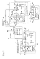
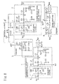
- FIG. 1 showing a circuit diagram of the high-frequency switch in this embodiment.
- a first transmission-reception switching circuit 1 switches between transmission and reception of a low-frequency-band signal (as specific example, EGSM signal in 900-MHz band).
- a low-frequency-band signal as specific example, EGSM signal in 900-MHz band.
- the anode of the first diode P1 is connected to the transmitting-circuit terminal Tx1 through the first capacitbr C1 and a low-pass filter 6 and the cathode of the first diode P1 is connected to the point A.
- one end of the first strip line L1 is connected to the joint between the first diode P1 and the low-pass filter 6 and the other end of the first strip line L1 is connected to the control terminal Vc1.
- the control terminal Vc1 serves as an input terminal for a control signal for switching between a transmission signal and a reception signal of the first transmission-reception switching circuit 1.
- the low-pass filter 6 is constituted by a parallel circuit comprising a fourteenth strip line L14 and a sixteenth capacitor C16, a fourteenth capacitor for connecting one end of the fourteenth strip line L14 to an earth, and a fifteenth capacitor C15 for connecting the other end of the fourteenth strip line L14 to an earth.
- the anode of the second diode P2 is connected to the receiving-circuit terminal Rx1 of the first transmission-reception switching circuit 1 through a series circuit comprising a surface-acoustic-wave filter (hereafter referred to as SAW filter) F3 and the fourth capacitor C4.
- SAW filter surface-acoustic-wave filter
- the cathode of the second diode P2 is connected to an earth through a parallel circuit comprising a fourth strip line L4 and the fifth capacitor C5.
- One end of the third strip line L3 is connected to the anode of the second diode P2 and the other end of the third strip line L3 is connected to the point A.
- the point A of the first transmission-reception switching circuit 1 is connected to a parallel circuit comprising the fifth strip line L5 of the first diplexer 3 and a twentieth capacitor C20 and the fifth strip line L5 and the other end of the twentieth capacitor C20 are connected to the antenna terminal ANT via the point C through the sixth capacitor C6. Moreover, one end of the fifth strip line L5 is connected to an earth through the seventh capacitor C7. In this case, the fifth strip line L5 of the first diplexer 3, the twentieth capacitor C20, and the seventh capacitor C7 constitute a low-pass filter. Moreover, the point C of the first diplexer 3 is connected to a matching circuit 8 through the thirteenth capacitor C13 and a twenty-first capacitor C21.
- the second transmission-reception switching circuit 2 switches between transmission and reception of high-frequency-band signals (as specific examples, DCS signal in 1,800-MHz band and PCS signal in 1,900-MHz band).
- the anode of a third diode P3 is connected to the transmitting-circuit terminal Tx2 of the second transmission-reception switching circuit 2 through an eighth capacitor C8 and a low-pass filter 7 and the cathode of the third diode P3 is connected to the point B.
- one end of a seventh strip line L7 is connected to the joint between the anode of the third diode P3 and the low-pass filter 7 and the other end of the seventh strip line L7 is connected to the control terminal Vc2.
- the control terminal Vc2 serves as an input terminal for a control signal for switching between a transmission signal and a reception signal of the second transmission-reception switching circuit 2.
- the anode of a fourth diode P4 is connected to receiving-circuit terminal Rx2 through an eleventh capacitor C11 and the cathode of the fourth diode P4 is connected to an earth through a parallel circuit comprising a tenth strip line L10 and a twelfth capacitor C12.
- One end of a ninth strip line L9 is connected to the anode of the fourth diode P4 and the other end of the ninth strip line L9 is connected to the point B.
- the point B of the second transmission-reception switching circuit 2 is connected to the thirteenth capacitor C13 of the first diplexer 3 via the matching circuit 8 and to the antenna terminal ANT through the sixth capacitor C6 by passing through the point C.
- One end of the thirteenth capacitor C13 is connected to an earth through a series circuit comprising the eleventh strip line L11 and the fourteenth capacitor C14.
- the thirteenth capacitor C13 of the first diplexer 3, eleventh strip line L11, and fourteenth capacitor C14 constitute a high-pass filter.
- a second diplexer 4 is constituted by a phase-shifting circuit 5 comprising strip lines L12 and L13, an SAW filter F1, and a SAW filter F2, in which the point D is connected to the receiving-circuit terminal Rx2 of the second transmission-reception switching circuit 2, the input terminal of the phase-shifting circuit 5 is connected to the point D, and the first output terminal of the phase-shifting circuit 5 is connected to the third receiving-circuit terminal Rx3 (PCS receiving terminal) through the first SAW filter F1. Moreover, the second output terminal of the phase-shifting circuit 5 isconnectedto the fourthreceiving-circuitterminal Rx4 (DCS receiving terminal) through the second SAW filter F2.
- the matching circuit 8 is provided to match the impedance of the second transmission-reception switching circuit 2 with that of the first diplexer 3 and one end of a sixteenth strip line L16 is grounded through a twenty-second capacitor C22. The other end of the sixteenth strip line L16 is connected to the point B grounded through a twenty-third capacitor C23 of the second transmission-reception switching circuit 2.
- the matching circuit 8 is not indispensable but it is sufficient to provide the circuit 8 when it is necessary to match impedances.
- the sixteenth strip line L16 or twenty-second capacitor C22 is unnecessary unless the matching circuit 8 is set.
- the antenna terminal ANT corresponds to an antenna terminal of the present invention.
- the transmitting-circuit terminal Tx1 corresponds to a first transmitting-circuit terminal of the present invention
- the receiving-circuit terminal Rx1 corresponds to a first receiving-circuit terminal of the present invention
- the first transmission-reception switching circuit 1 corresponds to a first transmission-reception switching circuit of the present invention.
- the transmitting-circuit terminal Tx2 corresponds to a second transmitting-circuit terminal of the present invention
- the receiving-circuit terminal Rx2 corresponds to a second receiving-circuit terminal of the present invention
- the second transmission-reception switching circuit 2 corresponds to a second transmission-reception switching circuit of the present invention.
- the first diplexer 3 corresponds to a first diplexer of the present invention.
- the phase-shifting circuit 5 corresponds to a phase-shifting circuit of the present invention
- the receiving-circuit terminal Rx3 corresponds to a third receiving-circuit terminal of the present invention
- the receiving-circuit terminal Rx4 corresponds to a fourth receiving-circuit terminal of the present invention
- the second diplexer 4 corresponds to a second diplexer of the present invention.
- means including the fifth strip line L5, seventh capacitor C7, and twentieth capacitor C20 corresponds to a low-pass filter disposed between an antenna terminal and a first transmission-reception switching circuit of the present invention.
- Means including the thirteenth capacitor C13, fourteenth capacitor C14, twenty-first capacitor C21, and eleventh strip line L11 correspond to a high-pass filter disposed between an antenna terminal and a second transmission-reception switching circuit of the present invention.
- the first diode P1 corresponds to a first diode of the present invention
- the second capacitor C2 correspondstoafirst(sic) capacitor of the present invention
- the control terminal Vc1 corresponds to a first control terminal of the present invention
- the first strip line L1 corresponds to a first strip line of the present invention
- the fifth capacitor C5 corresponds to a second capacitor of the present invention
- the fourth strip line L4 corresponds to a second strip line of the present invention
- the second diode P2 corresponds to a second diode of the present invention
- the third strip line L3 corresponds to a third strip line of the present invention.
- the third diode P3 corresponds to a third diode of the present invention
- the ninth capacitor C9 corresponds to a third capacitor of the present invention
- the control terminal Vc2 corresponds to a second control terminal of the present invention
- the seventh strip line L7 corresponds to a fourth strip line of the present invention
- the twelfth capacitor C12 corresponds to a fourth capacitor of the present invention
- the tenth strip line L10 corresponds to a fifth strip line of the present invention
- the fourth diode P4 corresponds to a fourth diode of the present invention
- the ninth strip line L9 corresponds to a sixth strip line of the present invention.
- the first SAW filter F1 corresponds to a first surface-acoustic-wave filter of the present invention
- the second SAW filter F2 corresponds to a second surface-acoustic-wave filter of the present invention
- the third SAW filter F3 corresponds to a third surface-acoustic-wave filter of the present invention.
- a low-pass filter for passing a signal in a low frequency band like the waveform 1 shown in FIG. 2 is formed by the fifth strip line L5, seventh capacitor C7, and twentieth capacitor C20 of the first diplexer 3 in FIG. 1 and an attenuation pole A is formed by a parallel circuit comprising the fifth strip line L5 and twentieth capacitor C20.
- a high-pass filter for passing a signal in a high frequency band like the waveform 2 shown in FIG. 2 is formed by the thirteenth capacitor C13, eleventh strip line L11, and fourteenth capacitor C14 and an attenuation pole B is formed by constituting a series circuit by the eleventh strip line L11 and fourteenth capacitor C14 connected to the earth side.
- the high-pass filter When transmitting or receiving a signal in a low frequency band by connecting it to an antenna through the above low-pass filter or high-pass filter, the high-pass filter preferably obtains an isolation for a low-frequency signal from the point C by the attenuation pole B and therefore, no signal leaks to the high-pass filter. Moreover, when transmitting or receiving a signal in a high frequency band, the low-pass filter preferably obtains an isolation from the point C for a high frequency by the attenuation pole A and therefore, no signal leaks to the low-pass filter. That is, the first diplexer 3 has a function for branching a low-frequency signal and a high-frequency signal.
- the first transmission-reception switching circuit 1 is described below.
- the first diode P1 and second diode P2 are turned on.
- the first capacitor C1, fourth capacitor C4, sixth capacitor C6, and thirteenth capacitor C13 prevent DC components, no DC current leaks to each terminal.
- the second diode P2 is connected to an earth, the impedance of the third strip line L3 infinitely increases. Therefore, a signal sent from the transmitting-circuit terminal Tx1 is not transferred to the receiving-circuit terminal Rx1.
- the transmission signal is sent to the antenna terminal ANT by passing through the low-pass filter of the first diplexer 3 via the point A.
- the low-pass filter 6 of the first transmission-reception switching circuit 1 prevents the harmonic component contained in a transmission signal from being transferred to the antenna terminal ANT. Because a transmission signal of the first transmission-reception switching circuit 1 is sent to the antenna terminal ANT by passing through the low-pass filter of the first diplexer 3, the low-pass filter 6 is not absolutely necessary. However, the filter 6 is used to further secure the effect of preventing the harmonic component.
- the first transmission-reception switching circuit 1 When the first transmission-reception switching circuit 1 performs reception, no DC voltage is applied to the control terminal Vc1. Therefore, because the first diode P1 and second diode P2 are turned off, a reception signal is transferred to the receiving-circuit terminal Rx1 via the point A from the antenna terminal ANT.
- a reception signal is transferred to the receiving-circuit terminal Rx1 via the point A from the antenna terminal ANT.
- the capacitance component of the first diode P1 by resonating the capacitance component of the first diode P1 with the second strip line L2 in order to avoid the influence of the capacitance component of the first diode P1, it is possible to make an isolation from the point A to the transmitting-circuit terminal Tx1 preferable at the reception frequency of a reception signal and transfer the reception signal from the antenna terminal ANT to the receiving-circuit terminal Rx1 through the low-pass filter of the first diplexer 3.
- the second transmission-reception switching circuit 2 is a circuit for transmitting or receiving a signal in a frequency band higher than that of the first transmission-reception switching circuit 1. Though the circuit configuration of the second transmission-reception switching circuit 2 is completely the same as that of the first transmission-reception switching circuit 1, the second transmission-reception switching circuit 2 is described below according to the accompanying drawings.
- the third diode P3 and fourth diode P4 are turned on by applying a positive voltage to the control terminal Vc2.
- the eighth capacitor C8, eleventh capacitor C11, thirteenth capacitor C13, and sixth capacitor C6 prevent DC components , no DC current flows through each terminal.
- the fourth diode P4 is connected to an earth and thereby, the impedance of the ninth strip line L9 infinitely increases, a signal sent from the transmitting-circuit terminal Tx2 is not transferred to the receiving-circuit terminal Rx2.
- the transmission signal is sent to the antenna terminal ANT via the point B by passing through the matching circuit 8 and the high-pass filter of the first diplexer 3.
- the low-pass filter 7 of the second transmission-reception switching circuit 2 prevents the harmonic component contained in a transmission signal from being transferred to the antenna terminal ANT. Because a transmission signal of the second transmission-reception switching circuit 2 is sent to the antenna terminal ANT by passing through the high-pass filter of the first diplexer 3 instead of passing through the low-pass filter of the circuit 3, it is preferable to use the low-pass filter 7 unless a transmission circuit takes secure measures for harmonics.
- the second diplexer 4 is described below.
- the point D is connected to the second receiving-circuit terminal Rx2 of the second transmission-reception switching circuit 2.
- the input terminal of the phase-shifting circuit 5 is connected to the point D and the first output terminal of the phase-shifting circuit 5 is connected to the third receiving-circuit terminal Rx3 through the first SAW filter F1.
- a band-pass filter for passing a reception signal in a second reception band specifically, a DCS-signal receiving band in 1,800-MHz band is constituted by the phase-shifting circuit 5 and first SAW filter F1 to pass only a reception signal in a low frequency band out of two types of high-band-frequency reception signals.
- the second output terminal of the phase-shifting circuit 5 is connected to the fourth receiving-circuit terminal Rx4 through the second SAW filter F2.
- a band-pass filter for passing a reception signal in a third reception band specifically, a PCS reception band in 1,900-MHz band is constituted by the phase-shifting circuit 5 and second SAW filter F2 to pass only a reception signal in a high frequency band out of two types of high-band-frequency reception signals.
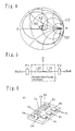
- FIG. 3 is a Smith chart showing the switch of impedances between the points D at the both ends of the single first SAW filter F1 and the terminal Rx3 when using a signal frequency as a parameter.
- the section along the curve between the points A1 and B1 on curves is a pass band of the first SAW filter F1, that is, the DCS side in 1,800-MHz band.
- the section along the curve between the points C1 and D1 on the curve is the pass band of the opposite side, that is, the PCS side in 1,900-MHz band.
- the pass band in the PCS band is separate from the central portion of the Smith chart to the upper side of the chart, it is also separate from the right side of the chart that is a high-impedance area.
- the first SAW filter F1 does not have an impedance high enough to prevent a PCS signal in 1,900-MHz band from passing. Therefore, in the case of the single first SAW filter F1, it is difficult to pass a signal in a DCS band in 1,800-MHz band and obtain a wave-filtering characteristic enough to prevent the PCS signal in 1,900-MHz band.
- FIG. 4 shows the impedance characteristic when using a signal frequency as a parameter in a diplexer in which the first output terminal of the phase-shifting circuit 5 and the first SAW filter f1 of the present invention are connected each other.
- FIG. 5 is a local circuit diagram in which the first output terminal of the phase-shifting circuit 5 and the first SAW filter F1 of the present invention are connected each other and the second output terminal of the phase-shifting circuit 5 and one end of the second SAW filter are connected each other.
- the input terminal of the phase-shifting circuit 5 is connected to the point D, the other end of the first SAW filter F1 is connected to the terminal Rx3, and the other end of the second SAW filter F2 is connected to the terminal Rx4.
- the Smith chart in FIG. 4 shows the impedance between the point D and the terminal Rx3 shown in FIG. 5. That is, the impedance curve in the case of the single SAW filter F1 shown in FIG. 3 has a shape shown in FIG. 4 because a phase is rotated by the phase-shifting circuit 5.
- the section along the curve between the points A2 and B2 on the curve is the pass band of the DCS side in 1,800-MHz band. Though the shape of the curve of the pass band of the DCS side slightly changes from that in FIG.
- the voltage standing-wave ratio (VSWR) is almost equal to 1, and it is shown that the series circuit comprising the phase-shifting circuit 5 and first SAW filter F1 connected between the point D and the terminal Rx3 matches with the impedance of a line.
- the section along the curve between the points C2 and D2 on the curve is the pass band of the PCS side in a 1,900 MHz band, in which the phase is rotated by the first phase-shifting circuit 5 and the pass band of the PCS side moves to a very-high-impedance area at the right side of the chart.
- the shape of a curve on a Smith chart is slightly changed.
- the position of the pass band of the PCS side in 1,900-MHz band is brought to almost the center of the Smith chart and the position of the pass band of the DCS side in 1,800-MHz band is separate from the center of the Smith chart.
- the pass band of the DCS in 1,800-MHz band is separate from the right side of the Smith chart having a high impedance, the filtering characteristic of passing only PCS signals in 1,90-MHz band and sufficiently preventing DCS signals in 1,800-MHz band cannot be not obtained.
- phase-shifting circuit 5 is described above by using a circuit constituted by strip lines as an example, a phase-shifting circuit can be constituted by various configurations. Therefore, a phase-shifting circuit of the present invention is not restricted to a circuit constituted by strip lines.
- a phase-shifting circuit has a strip line SL51 connected at one end to the second receiving-circuit terminal Rx2 (refer to FIG. 1) and connected at the other end to the SAW filter F1, a capacitor C51 connected at one end to the second receiving-circuit terminal Rx2 and grounded at the other end through an inductor L51, and a capacitor C52 grounded at one end through the inductor L51 and connected to the capacitor C51 and connected at the other end to the SAW filter F2 (the laminated structure of a laminated high-frequency switch using the above phase-shifting circuit will be described later).
- the strip line SL51 corresponds to the seventh strip line of the present invention
- the inductor L51 corresponds to the first inductor of the present invention
- the capacitor C51 corresponds to the fifth capacitor of the present invention
- the capacitor C52 corresponds to the sixth capacitor of the present invention.
- a phase-shifting circuit has an inductor L61 grounded at one end through a capacitor C61 and connected to the second receiving-circuit terminal Rx2 and connected at the other end to the SAW filter F1, a capacitor C62 connected at one end to the receiving-circuit terminal Rx2 and grounded at the other end through an inductor L62, and a capacitor C63 grounded at one end through the inductor L62 and connected to the capacitor C62 and connected at the other end to the SAW filter F2.
- the capacitor C61 corresponds to the seventh capacitor of the present invention
- the inductor L61 corresponds to the second inductor of the present invention
- the inductorL62 corresponds to the third inductor of the present invention
- the capacitor C62 corresponds to the eighth capacitor of the present invention
- the capacitor C63 corresponds to the ninth capacitor of the present invention.
- the diplexer 4 is used which distinguishes between signals in two frequency bands as a circuit characteristic instead of the auxiliary switching circuit 14 for switching between signals in two frequency bands through control differently from the case of a conventional high-frequency switch, it is possible to reduce the number of components to be mounted on the surface of a laminated substrate constituting a high-frequency switch and omit two diodes which particularly require mounting spaces and to which a standby voltage must be applied.
- reception signals of two different high-frequency bands are switchedby the phase-shifting circuit 5 of the second diplexer 4 and the surface-acoustic-wave filters F1 and F2, it is unnecessary to control the second diplexer 4 by applying a control voltage to the circuit 4 from an external unit and unnecessary to apply a standby voltage even under reception standby. Therefore, it is possible to reduce power consumption.
- a first diplexer is constituted by a low-pass filter and a high-pass filter.
- this embodiment is not restricted to the above case. It is also possible to realize this embodiment by using a band-pass filter having the same pass band as a low-pass filter or high-pass filter.
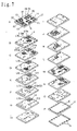
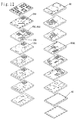
- Fig 6 is an exploded perspective view of the laminated high-frequency switch in the embodiment 2 of the present invention.
- the structure of the high-frequency switch in the above first embodiment is also described below.
- FIG. 6 shows a laminate using the high-frequency switch in the first embodiment.
- Three SAW filters F1, F2, and F3 and four diodes P1 to P4, and capacitors C1, C6, and C8 respectively having a comparatively large capacity aremounted on the upper face of a laminated high-frequency switch 21 having a multilayer structure in which various strip lines and capacitors constituting the high-frequency switch are built through terminals T1 formed on the upper face of the laminated high-frequency switch 21 and electrically connected to internal circuits of the laminated high-frequency switch 21.
- FIG. 7 is an exploded perspective view of the above laminated high-frequency switch 21.
- the high-frequency switch in this embodiment is constituted by 16-layer dielectric substrates 21A to 21P and the laminated number of dielectric substrates is not restricted to the configuration in this embodiment but it is properly selected in accordance with a characteristic required for the high-frequency switch.
- a dielectric substrate can use the so-called glass-ceramics substrate obtained by adding low-melting glass frit to ceramic powder such as forsterite. Many via holes for electrically connecting multilayer wirings each other are drilled on a green sheet obtained by forming the slurry obtained by adding an organic binder and an organic solvent to the ceramic powder by means of punching or laser working.
- strip lines L1 to L14 and capacitor electrodes C1 to C23 shown in FIG. 1 are printed on predetermined green sheets by using conductive paste whose conductive material mainly contains silver, gold, or copper powder to form a wiring pattern and printing-inject the same conductive paste into via holes for inter-layer-connecting the wiring pattern of each green sheet.
- the laminated high-frequency switch 21 can be obtained by drying the above obtained laminate, then baking the laminate in a kiln having an oxidation atmosphere at approx. 400 to 500°C to burn out the organic binder in the green sheets, then baking the laminate in the normal air when using silver or gold powder as the main component of a conductive material or in an inert-gas atmosphere or a reducing atmosphere in a temperature range of approx. 850 to 950°C when using copper powder.
- a plurality of terminals T1 for mounting SAW filters and diodes are provided on the upper face of the dielectric substrate 21A and a plurality of terminals T2 for mounting a high-frequency switch of the present invention on the surface of the main substrate of electronic units are provided on the back of the dielectric substrate 21P on whose surface an earth electrode E is formed by printing and patterning the above conductive paste.
- the laminated structure of the wiring pattern of a high-frequency switch having the multilayer structure thus constituted is briefly described below by illustrating the fourth and tenth strip lines and the thirteenth and twenty-first capacitors.
- the tenth strip line L10 and the fourth strip line L4 are constituted by successively connecting the lines L10 and L4 over six layers to the strip line patterns on the dielectric substrate 21G through via holes respectively so that strip line patterns on the dielectric substrate 21B are inter-layer-connected to strip line patterns on the dielectric substrate 21C through via holes 21B 10 and 21B 4 and strip line patterns on the dielectric substrate 21C are inter-layer-connected to strip line patterns on the dielectric substrate 21D through via holes 21C 10 and 21C 4 .
- the thirteenth capacitor C13 and twenty-first capacitor C21 are constituted in series by providing the electrode pattern of the twenty-first capacitor C21 for the dielectric substrate 21E and the electrode pattern shared by the thirteenth capacitor C13 and twenty-first capacitor C21 for the dielectric substrate 21F, and then the electrode pattern of the thirteenth capacitor C13 for the dielectric substrate 21G.
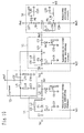
- FIG. 8 showing a circuit diagram of the high-frequency switch in this embodiment. Because the circuit diagram shown in FIG. 8 is basically the same as the circuit diagram in the first embodiment shown in FIG. 1, points different from the configuration shown in FIG. 1 are described below.
- balun balanced-to-unbalanced converters BL1 and BL2 (hereafter respectively referred to as balun) are connected between the first output terminal of the phase-shifting circuit 5 of the second diplexer 4 and the first SAW filter F1 and between the second output terminal of the phase-shifting circuit 5 of the diplexer 4 and the second SAW filter F2.
- a balun is disposed at the input side of the SAW filter F3 connected to the first receiving-circuit terminal Rx1, that is, between the anode of the second diode P2 of the first transmission-reception switching circuit 1 and the SAW filter F3.
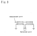
- FIG. 9 shows an equivalent circuit of a balun.
- a balun When a signal is input to an unbalanced port of the balun, a balanced output of the signal is obtained from a balanced port.
- a balun it is possible to convert an output signal of a receiving-circuit terminal into a balanced output by a simple circuit configuration and realize a circuit configuration strong for noises.
- a balun is constituted as shown in FIG. 9, it is possible to omit DC-cutoff capacities for cutting off a DC connected to the receiving-circuit terminals Rx1 and Rx2, that is, it is possible to omit the fourth capacitor C4 and eleventh capacitor C11 shown in FIG. 1 in order to cut off a DC.
- the balanced-to-unbalanced converter BL1 correspond to the first balanced-to-unbalanced converter of the present invention and the balanced-to-unbalanced converter BL2 corresponds to the second balanced-to-unbalanced converter of the present invention.
- the balun disposed between the anode of the second diode P2 of the first transmission-reception switching circuit 1 and the SAW filter F3 corresponds to the third balanced-to-unbalanced converter of the present invention.
- the configuration of the high-frequency switch in the third embodiment can be formed by a configuration same as the case of the second embodiment.
- the present invention includes a high-frequency switch provided with (1) a first transmission-reception switching circuit for selectively switching between the signal transfer between an antenna terminal and a first transmitting-circuit terminal and the signal transfer between the antenna terminal and a first receiving-circuit terminal, (2) a second transmission-reception switching circuit for selectively switching between the signal transfer between the antenna terminal and a second transmitting-circuit terminal and the signal transfer between the antenna terminal and a second receiving-circuit terminal, (3) a first diplexer disposed between the antenna terminal and the first transmission-reception switching circuit and between the antenna terminal and the second transmission-reception switching circuit, (4) a second diplexer connected to the second receiving-circuit terminal in order to selectively switch the signal transfer between the second receiving-circuit terminal and a third receiving-circuit terminal and the signal transfer between the second receiving-circuit terminal and a fourth receiving-circuit terminal by using a phase-shifting circuit and a surface-acoustic-wave filter, and (5) a third diplex
- This type of the high-frequency switch has a configuration in which a diplexer similar to the diplexer 4 (refer to FIG. 1) is connected to the receiving-circuit terminal Rx1 (refer to FIG. 1) of the high-frequency switch in the embodiment 1 described above as the above third diplexer, which can be used for a portable telephone corresponding to four bands capable of branching four frequencies.
- the present invention includes a high-frequency radio unit provided with a transmitting circuit for performing transmission, a receiving circuit for performing reception, and the above high-frequency switch.
- a high-frequency switch of the present invention has the following advantages.
- balun By using a balun, it is possible to reduce a capacity for DC cutoff connected to a receiving-circuit terminal. Moreover, by using a balun and thereby obtaining a balanced output, it is possible to realize a circuit strong for noises.
- the present invention has an advantage that it is possible to reduce the number of components to be mounted on the surface of the laminated substrate of a high-frequency switch.
- the present invention has an advantage that it is possible to reduce the power consumption of a high-frequency switch.
Landscapes
- Transceivers (AREA)
- Waveguide Switches, Polarizers, And Phase Shifters (AREA)
- Electronic Switches (AREA)
Applications Claiming Priority (2)
| Application Number | Priority Date | Filing Date | Title |
|---|---|---|---|
| JP2000394292 | 2000-12-26 | ||
| JP2000394292 | 2000-12-26 |
Publications (2)
| Publication Number | Publication Date |
|---|---|
| EP1223634A2 true EP1223634A2 (de) | 2002-07-17 |
| EP1223634A3 EP1223634A3 (de) | 2003-08-13 |
Family
ID=18859940
Family Applications (1)
| Application Number | Title | Priority Date | Filing Date |
|---|---|---|---|
| EP01130694A Withdrawn EP1223634A3 (de) | 2000-12-26 | 2001-12-21 | Hochfrequenzschalter, laminierter Hochfrequenzschalter, Hochfrequenz-Funkeinheit und Hochfrequenz-Schaltverfahren |
Country Status (3)
| Country | Link |
|---|---|
| US (3) | US6606015B2 (de) |
| EP (1) | EP1223634A3 (de) |
| CN (2) | CN1241325C (de) |
Cited By (8)
| Publication number | Priority date | Publication date | Assignee | Title |
|---|---|---|---|---|
| US6563396B2 (en) * | 1999-09-28 | 2003-05-13 | Murata Manufacturing Co., Ltd. | Composite high frequency component and mobile communication apparatus incorporating the same |
| EP1401045A1 (de) * | 2002-09-17 | 2004-03-24 | Hitachi Metals, Ltd. | Hochfrequenzvorrichtung,Hochfrequenzmodul und damit versehenes Kommunikationsgerät |
| EP1453135A1 (de) * | 2003-02-26 | 2004-09-01 | Matsuhita Electric Industrial Co., Ltd. | Antennenschaltmodul, allesenthaltendes Kommunikationsmodul, Kommunikationsgerät und Herstellungsverfahren für ein Antennenschaltmodul |
| KR100496499B1 (ko) * | 2001-11-12 | 2005-06-22 | 마쯔시다덴기산교 가부시키가이샤 | 다이플렉서, 이를 사용하는 고주파수 스위치 및 안테나 듀플렉서 |
| US7239853B2 (en) | 2002-12-06 | 2007-07-03 | Tdk Corporation | Antenna switching circuit |
| EP1601112A4 (de) * | 2003-02-14 | 2007-09-12 | Tdk Corp | Frontendmodul |
| CN101542924B (zh) * | 2007-05-10 | 2012-12-05 | 株式会社村田制作所 | 复合高频器件 |
| EP2757686A1 (de) * | 2013-01-18 | 2014-07-23 | Murata Manufacturing Co., Ltd. | Filterkreislauf |
Families Citing this family (40)
| Publication number | Priority date | Publication date | Assignee | Title |
|---|---|---|---|---|
| WO2002017504A1 (en) * | 2000-08-22 | 2002-02-28 | Hitachi Metals, Ltd. | Laminated high-frequency switch module |
| JP2002118486A (ja) * | 2000-10-06 | 2002-04-19 | Matsushita Electric Ind Co Ltd | 高周波複合スイッチモジュール |
| JP3800504B2 (ja) * | 2001-05-15 | 2006-07-26 | Tdk株式会社 | フロントエンドモジュール |
| JP3874241B2 (ja) * | 2001-07-27 | 2007-01-31 | 株式会社ルネサステクノロジ | 電子部品および設計方法 |
| US6995630B2 (en) * | 2001-10-24 | 2006-02-07 | Matsushita Electric Industrial Co., Ltd. | High-frequency compound switch module and communication terminal using it |
| CN100536328C (zh) * | 2002-10-25 | 2009-09-02 | 日立金属株式会社 | 平衡-不平衡型多频带滤波模块 |
| JP2004153523A (ja) * | 2002-10-30 | 2004-05-27 | Matsushita Electric Ind Co Ltd | 高周波スイッチモジュール |
| KR101031692B1 (ko) * | 2002-12-18 | 2011-04-29 | 파나소닉 주식회사 | 무선 통신 장치, 무선 통신 방법, 안테나 장치 및 제 1듀플렉서 |
| US7295814B2 (en) * | 2003-02-05 | 2007-11-13 | Hitachi Metals, Ltd. | Antenna switch circuit and antenna switch module |
| WO2004073193A1 (ja) * | 2003-02-14 | 2004-08-26 | Hitachi Metals, Ltd. | スイッチ回路及び複合高周波部品 |
| US6873225B2 (en) * | 2003-04-15 | 2005-03-29 | Microphase Corporation | Diplexers with low pass filter having distributed and non-distributed (lumped) elements |
| US7049906B2 (en) * | 2003-05-29 | 2006-05-23 | Sony Ericsson Mobile Communications Ab | Quad band antenna interface modules including matching network ports |
| JP4029779B2 (ja) * | 2003-06-05 | 2008-01-09 | 株式会社村田製作所 | 高周波モジュールおよび通信装置 |
| JP2005006072A (ja) * | 2003-06-12 | 2005-01-06 | Matsushita Electric Ind Co Ltd | 高周波スイッチ装置および半導体装置 |
| JP2005006143A (ja) * | 2003-06-13 | 2005-01-06 | Matsushita Electric Ind Co Ltd | 高周波スイッチ回路および半導体装置 |
| EP1515450B1 (de) * | 2003-08-15 | 2007-08-15 | TDK Corporation | Antennenumschaltungsvorrichtung |
| JP4042860B2 (ja) * | 2003-12-05 | 2008-02-06 | 太陽誘電株式会社 | バラン |
| DE102004001347B3 (de) * | 2004-01-08 | 2005-07-07 | Epcos Ag | Duplexer mit niedriger Bauhöhe |
| EP1796276A4 (de) * | 2004-06-07 | 2012-03-14 | Hitachi Metals Ltd | Hochfrequenz-schaltmodul und verfahren zu seiner steuerung |
| WO2006003959A1 (ja) * | 2004-06-30 | 2006-01-12 | Hitachi Metals, Ltd. | 高周波回路、高周波部品及びマルチバンド通信装置 |
| JPWO2006013753A1 (ja) * | 2004-08-06 | 2008-05-01 | 株式会社村田製作所 | 高周波複合部品 |
| JP4134004B2 (ja) * | 2004-11-15 | 2008-08-13 | Tdk株式会社 | 高周波モジュール |
| JP4446922B2 (ja) * | 2005-04-21 | 2010-04-07 | 富士通メディアデバイス株式会社 | フィルタおよび分波器 |
| EP1876722B1 (de) * | 2005-04-28 | 2016-08-24 | Murata Manufacturing Co., Ltd. | Hochfrequenzschaltmodul und verfahren zur anpassung der frequenzmerkmale einer hochfrequenzschaltung |
| DE102005020086B4 (de) * | 2005-04-29 | 2013-07-11 | Epcos Ag | Elektrisches Multiband-Bauelement |
| US20070030095A1 (en) * | 2005-08-05 | 2007-02-08 | Mitsutaka Hikita | Antenna duplexer and wireless terminal using the same |
| TW200713681A (en) * | 2005-09-26 | 2007-04-01 | Murata Manufacturing Co | High-frequency front end module, and duplexer |
| WO2008013170A1 (en) * | 2006-07-25 | 2008-01-31 | Murata Manufacturing Co., Ltd. | High frequency module and communication apparatus using same |
| JP2008109535A (ja) * | 2006-10-27 | 2008-05-08 | Hitachi Media Electoronics Co Ltd | スイッチ回路、それを有するフロントエンドモジュール及び無線端末 |
| US20080102762A1 (en) * | 2006-10-30 | 2008-05-01 | Lianjun Liu | Methods and apparatus for a hybrid antenna switching system |
| TWI442621B (zh) * | 2007-01-19 | 2014-06-21 | Murata Manufacturing Co | High frequency parts |
| JP4379542B2 (ja) * | 2007-03-16 | 2009-12-09 | パナソニック株式会社 | 弾性表面波デバイス |
| JP4873046B2 (ja) * | 2009-05-26 | 2012-02-08 | 株式会社村田製作所 | 高周波モジュール |
| JP5293762B2 (ja) * | 2011-03-04 | 2013-09-18 | 株式会社村田製作所 | 高周波スイッチモジュール |
| JP6114198B2 (ja) * | 2011-11-28 | 2017-04-12 | スカイワークスフィルターソリューションズジャパン株式会社 | 高周波フィルタ |
| JP6010350B2 (ja) * | 2012-06-04 | 2016-10-19 | 太陽誘電株式会社 | 弾性波デバイス |
| US9071388B2 (en) * | 2012-08-03 | 2015-06-30 | Entropic Communications, LLC. | Switchable diplexer with physical layout to provide improved isolation |
| CN103944527B (zh) * | 2014-04-15 | 2017-03-08 | 华为技术有限公司 | 一种高通滤波器电路及集成电路 |
| CN104022745B (zh) * | 2014-06-03 | 2017-01-25 | 成都嘉晨科技有限公司 | 超宽频带大功率功放器件 |
| RU178443U1 (ru) * | 2017-07-26 | 2018-04-04 | Акционерное Общество "Светлана-Электронприбор" | Сверхширокополосный автономный антенный переключатель для коротких видеоимпульсов |
Citations (2)
| Publication number | Priority date | Publication date | Assignee | Title |
|---|---|---|---|---|
| EP1014592A2 (de) | 1998-12-22 | 2000-06-28 | Hitachi Media Electronics Co., Ltd. | Mobilfunkendgerät und Oberflächewellenantenneduplexer |
| WO2001048935A1 (en) | 1999-12-28 | 2001-07-05 | Hitachi Metals, Ltd. | High-frequency switch, high-frequency switch module, and wireless communication device |
Family Cites Families (8)
| Publication number | Priority date | Publication date | Assignee | Title |
|---|---|---|---|---|
| US3768043A (en) * | 1973-01-05 | 1973-10-23 | Rca Corp | Wideband hybrid system |
| US5933770A (en) * | 1995-11-27 | 1999-08-03 | Lucent Technologies Inc. | Low distortion tuner-receiver with bridge-type diplexer |
| JPH11154804A (ja) * | 1997-11-20 | 1999-06-08 | Hitachi Ltd | 高周波回路装置 |
| EP1650865B1 (de) * | 1998-10-27 | 2009-10-21 | Murata Manufacturing Co., Ltd. | Zusammengestellte Hochfrequenzkomponente und damit ausgerüstetes mobiles Kommunikationsgerät |
| JP3304898B2 (ja) * | 1998-11-20 | 2002-07-22 | 株式会社村田製作所 | 複合高周波部品及びそれを用いた移動体通信装置 |
| JP2002064301A (ja) * | 1999-03-18 | 2002-02-28 | Hitachi Metals Ltd | トリプルバンド用高周波スイッチモジュール |
| JP3456164B2 (ja) * | 1999-06-02 | 2003-10-14 | 三菱電機株式会社 | アンテナ給電装置 |
| JP3711846B2 (ja) * | 2000-07-27 | 2005-11-02 | 株式会社村田製作所 | 高周波モジュール及びそれを用いた移動体通信装置 |
-
2001
- 2001-12-21 EP EP01130694A patent/EP1223634A3/de not_active Withdrawn
- 2001-12-26 CN CN01145221.8A patent/CN1241325C/zh not_active Expired - Fee Related
- 2001-12-26 CN CN200510131684.XA patent/CN1819453A/zh not_active Withdrawn
- 2001-12-26 US US10/034,879 patent/US6606015B2/en not_active Expired - Lifetime
-
2003
- 2003-06-17 US US10/463,005 patent/US6867662B2/en not_active Expired - Fee Related
-
2005
- 2005-02-02 US US11/049,440 patent/US7023296B2/en not_active Expired - Fee Related
Patent Citations (2)
| Publication number | Priority date | Publication date | Assignee | Title |
|---|---|---|---|---|
| EP1014592A2 (de) | 1998-12-22 | 2000-06-28 | Hitachi Media Electronics Co., Ltd. | Mobilfunkendgerät und Oberflächewellenantenneduplexer |
| WO2001048935A1 (en) | 1999-12-28 | 2001-07-05 | Hitachi Metals, Ltd. | High-frequency switch, high-frequency switch module, and wireless communication device |
Cited By (15)
| Publication number | Priority date | Publication date | Assignee | Title |
|---|---|---|---|---|
| US6563396B2 (en) * | 1999-09-28 | 2003-05-13 | Murata Manufacturing Co., Ltd. | Composite high frequency component and mobile communication apparatus incorporating the same |
| KR100496499B1 (ko) * | 2001-11-12 | 2005-06-22 | 마쯔시다덴기산교 가부시키가이샤 | 다이플렉서, 이를 사용하는 고주파수 스위치 및 안테나 듀플렉서 |
| US7577404B2 (en) | 2002-09-17 | 2009-08-18 | Hitachi Metals, Ltd. | High-frequency device, high-frequency module and communications device comprising them |
| US7076216B2 (en) | 2002-09-17 | 2006-07-11 | Hitachi Metals, Ltd. | High-frequency device, high-frequency module and communications device comprising them |
| EP1401045A1 (de) * | 2002-09-17 | 2004-03-24 | Hitachi Metals, Ltd. | Hochfrequenzvorrichtung,Hochfrequenzmodul und damit versehenes Kommunikationsgerät |
| KR101031836B1 (ko) | 2002-09-17 | 2011-05-02 | 히타치 긴조쿠 가부시키가이샤 | 고주파 부품 및 고주파 모듈 및 이들을 사용한 통신기 |
| EP2287963A3 (de) * | 2002-09-17 | 2011-06-08 | Hitachi Metals, Ltd. | Hochfrequenzvorrichtung, Hochfrequenzmodul und damit versehenes Kommunikationsgerät |
| US7239853B2 (en) | 2002-12-06 | 2007-07-03 | Tdk Corporation | Antenna switching circuit |
| EP1601112A4 (de) * | 2003-02-14 | 2007-09-12 | Tdk Corp | Frontendmodul |
| US7420438B2 (en) | 2003-02-14 | 2008-09-02 | Tdk Corporation | Front end module |
| EP1453135A1 (de) * | 2003-02-26 | 2004-09-01 | Matsuhita Electric Industrial Co., Ltd. | Antennenschaltmodul, allesenthaltendes Kommunikationsmodul, Kommunikationsgerät und Herstellungsverfahren für ein Antennenschaltmodul |
| US6975271B2 (en) | 2003-02-26 | 2005-12-13 | Matsushita Electric Industrial Co., Ltd. | Antenna switch module, all-in-one communication module, communication apparatus and method for manufacturing antenna switch module |
| CN101542924B (zh) * | 2007-05-10 | 2012-12-05 | 株式会社村田制作所 | 复合高频器件 |
| EP2757686A1 (de) * | 2013-01-18 | 2014-07-23 | Murata Manufacturing Co., Ltd. | Filterkreislauf |
| US9331658B2 (en) | 2013-01-18 | 2016-05-03 | Murata Manufacturing Co., Ltd. | Filter circuit |
Also Published As
| Publication number | Publication date |
|---|---|
| CN1362786A (zh) | 2002-08-07 |
| US6606015B2 (en) | 2003-08-12 |
| EP1223634A3 (de) | 2003-08-13 |
| US20030214367A1 (en) | 2003-11-20 |
| US7023296B2 (en) | 2006-04-04 |
| CN1819453A (zh) | 2006-08-16 |
| US6867662B2 (en) | 2005-03-15 |
| CN1241325C (zh) | 2006-02-08 |
| US20050134402A1 (en) | 2005-06-23 |
| US20020101296A1 (en) | 2002-08-01 |
Similar Documents
| Publication | Publication Date | Title |
|---|---|---|
| US6606015B2 (en) | High-frequency switch, laminated high-frequency switch, high-frequency radio unit, and high frequency switching method | |
| JP4324807B2 (ja) | 高周波スイッチモジュール | |
| US6788958B2 (en) | High-frequency module and mobile communication apparatus using the same | |
| US6987984B1 (en) | High-frequency switch module | |
| JP5187361B2 (ja) | 高周波モジュール | |
| EP1378958A1 (de) | Zusammengestellte Hochfrequenzvorrichtung | |
| JP4221205B2 (ja) | ダイプレクサ並びにそれを用いた高周波スイッチ | |
| EP0785590A1 (de) | Zusammengestellte Hochfrequenzkomponente | |
| US6882250B2 (en) | High-frequency device and communication apparatus | |
| US7904030B2 (en) | High frequency switch, radio communication apparatus, and high frequency switching method | |
| US7027777B2 (en) | High frequency switch and high frequency radio communication apparatus | |
| US5999065A (en) | Composite high-frequency component | |
| JP2002261651A (ja) | 高周波スイッチ、高周波スイッチ積層体、高周波無線機器、および高周波スイッチング方法 | |
| JP2003204284A (ja) | 高周波スイッチ、および高周波無線機器 | |
| JP3926186B2 (ja) | 高周波スイッチ、および無線通信機器 | |
| JP2001168670A (ja) | 高周波部品及びそれを用いた移動体通信装置 | |
| JPH11274876A (ja) | ローパスフィルタおよび回路基板 | |
| JP2003078443A (ja) | 高周波スイッチ回路 | |
| JP2003078438A (ja) | 複合高周波回路部品 | |
| GB2395612A (en) | Laminated LC low-pass filter with trap circuit |
Legal Events
| Date | Code | Title | Description |
|---|---|---|---|
| PUAI | Public reference made under article 153(3) epc to a published international application that has entered the european phase |
Free format text: ORIGINAL CODE: 0009012 |
|
| AK | Designated contracting states |
Kind code of ref document: A2 Designated state(s): AT BE CH CY DE DK ES FI FR GB GR IE IT LI LU MC NL PT SE TR |
|
| AX | Request for extension of the european patent |
Free format text: AL;LT;LV;MK;RO;SI |
|
| PUAL | Search report despatched |
Free format text: ORIGINAL CODE: 0009013 |
|
| AK | Designated contracting states |
Designated state(s): AT BE CH CY DE DK ES FI FR GB GR IE IT LI LU MC NL PT SE TR |
|
| AX | Request for extension of the european patent |
Extension state: AL LT LV MK RO SI |
|
| 17P | Request for examination filed |
Effective date: 20030813 |
|
| TPAC | Observations filed by third parties |
Free format text: ORIGINAL CODE: EPIDOSNTIPA |
|
| TPAC | Observations filed by third parties |
Free format text: ORIGINAL CODE: EPIDOSNTIPA |
|
| AKX | Designation fees paid |
Designated state(s): DE FR GB |
|
| STAA | Information on the status of an ep patent application or granted ep patent |
Free format text: STATUS: THE APPLICATION HAS BEEN WITHDRAWN |
|
| 17Q | First examination report despatched |
Effective date: 20060724 |
|
| 18W | Application withdrawn |
Effective date: 20060726 |