EP1014770A2 - Abgeschirmtes Modulgehäuse für Substrate - Google Patents
Abgeschirmtes Modulgehäuse für Substrate Download PDFInfo
- Publication number
- EP1014770A2 EP1014770A2 EP99403159A EP99403159A EP1014770A2 EP 1014770 A2 EP1014770 A2 EP 1014770A2 EP 99403159 A EP99403159 A EP 99403159A EP 99403159 A EP99403159 A EP 99403159A EP 1014770 A2 EP1014770 A2 EP 1014770A2
- Authority
- EP
- European Patent Office
- Prior art keywords
- housing
- substrate
- parts
- housing according
- spacers
- Prior art date
- Legal status (The legal status is an assumption and is not a legal conclusion. Google has not performed a legal analysis and makes no representation as to the accuracy of the status listed.)
- Granted
Links
Images


Classifications
-
- H—ELECTRICITY
- H05—ELECTRIC TECHNIQUES NOT OTHERWISE PROVIDED FOR
- H05K—PRINTED CIRCUITS; CASINGS OR CONSTRUCTIONAL DETAILS OF ELECTRIC APPARATUS; MANUFACTURE OF ASSEMBLAGES OF ELECTRICAL COMPONENTS
- H05K9/00—Screening of apparatus or components against electric or magnetic fields
- H05K9/0007—Casings
- H05K9/002—Casings with localised screening
- H05K9/0022—Casings with localised screening of components mounted on printed circuit boards [PCB]
-
- H—ELECTRICITY
- H05—ELECTRIC TECHNIQUES NOT OTHERWISE PROVIDED FOR
- H05K—PRINTED CIRCUITS; CASINGS OR CONSTRUCTIONAL DETAILS OF ELECTRIC APPARATUS; MANUFACTURE OF ASSEMBLAGES OF ELECTRICAL COMPONENTS
- H05K7/00—Constructional details common to different types of electric apparatus
- H05K7/14—Mounting supporting structure in casing or on frame or rack
- H05K7/1417—Mounting supporting structure in casing or on frame or rack having securing means for mounting boards, plates or wiring boards
- H05K7/142—Spacers not being card guides
Definitions
- the present invention relates to a modular housing for a substrate with electronic components, wherein the housing comprises at least a base part and a cover part, wherein the parts of the housing consist of an electrically conductive material for electromagnetic shielding and form outer walls enclosing a space inside the housing which accommodates the substrate, wherein dividing walls extend in the space inside the housing and have free edges which support the substrate.
- a housing which consists of an electrically conductive material for electromagnetic shielding.
- the housing consists generally of two or more parts which are fixed to each other by connection means, for example screws.
- a housing with dividing walls inside the space for the substrate is described in US patent 4,661,888.
- the housing consists of a base plate and two cover plates on opposite sides of the base. Both the base and the covers have dividing walls supporting a substrate which is located between the base and a cover. The free edges of the dividing walls contact continuous grounding strip conductors on the substrate. In this way, different sections of the substrate are shielded against each other.
- the contact between the walls and the conducting strips is improved by conductive elastomer gaskets which are disposed on the edges of the walls.
- the connecting means press the parts of the housing onto the opposing sides of the substrate, i. e. the substrate separates the parts from each other. Consequently, the mechanical stability of the housing is limited by the properties of the substrate. In most cases, the thermal expansion coefficients of the housing and the substrate differ. This causes mechanical stress which may lead to damage of the electronic circuits on the substrate when the housing is subject to temperature changes resulting from external influences or heat generation from components inside. Mechanical stress can also be caused by tolerances in the dimensions of the parts or improper fixing of the parts to each other. Finally, in the state of the art the cooling of the components in the housing is achieved by air circulation through holes in the outer walls which impair the shielding. However, thermal air circulation is not possible for space applications. Consequently, other means for heat dissipation have to be developed.
- At least one of said parts is provided with spacers which are in mechanical and thermal contact with an adjacent part and which define the height of the space inside the housing.
- the basic concept of the invention is to provide spacers which extend through the space inside the housing.
- the spacers form a continuous mechanical and thermal connection between adjacent parts of the housing. Consequently, they define the height of the space inside.
- the free space is dimensioned to accommodate the substrate with the electronic components.
- the spacers ensure that there is a gap between the dividing walls on opposing sides of a substrate and the width of the gap is at least equal to the thickness of the substrate.
- a preferred shape of the parts are slices aligned parallel to the substrates.
- connections from the substrates to elements outside of the housing or between different substrates are obtained preferably by flexible or semi-flexible connections.
- sliding connections may be used.
- connections from the housing to outside components are located only on one of its parts, preferably on the base part. This allows to open the housing, e.g. for service or adjustment, by removal of the cover while leaving the connections in place.
- one of its parts, preferably the base can be coupled to a supporting structure which dissipates the heat.
- the proposed design has the advantage that mechanical forces on the housing, especially pressures, are not transferred to the substrate inside but rather by the spacers between the outer walls. Furthermore, the spacers conduct heat generated inside the housing by thermal contact to its outer walls. Because the spacers in conjunction with the dividing walls improve the stability of the housing, the weight may be low while retaining a good stability.
- the housing comprises one or more intermediate parts located between the base part and the cover part.
- a substrate can be located in a gap between the base part and an intermediate part, between the cover part and an intermediate part or between two intermediate parts.
- the modular construction offers the opportunity to adapt the size of the housing to different numbers of substrates by using different numbers of intermediate parts.
- the intermediate parts are provided with dividing walls for supporting one or several substrates.
- the intermediate parts are also provided with spacers for defining the height of the space inside the housing, especially the width of the gaps for accommodating the substrates.
- the parts of the housing are one-piece parts comprising the outer walls, the dividing walls and the spacers.
- the parts may either be machined parts or castings, facilitating a suitable shape and size of the housing.
- a good electrical conductivity and a low mass of the housing can be attained by parts made from aluminium or a magnesium alloy.
- the spacers may be located exclusively on one of the adjacent parts and extend all the way through the space inside the housing to the outer wall of another part. It is preferred, however, that a spacer touches the face of another spacer in the adjacent part of the housing. In this case, the spacers are segments of a larger mechanical and thermal connection through the housing.
- Fastening means are of advantage to join different parts of the housing to each other and the housing to a support. Suitable means are for example screws or pin screws.
- some or all spacers include a hole to accommodate the fastening means.
- the location of the fastening means inside the spacers reduces strains in the housing.
- a good thermal and mechanical contact between the spacer and an adjacent part of the housing, especially between adjacent spacers is ensured.
- continuous holes running through the whole housing are preferred. It is, however, possible that holes extend only through a part of a spacer. If screws are used as a fastening means, the inner surfaces of the holes may be threaded.
- the spacers can be located at any position inside the housing which is suitable to attain a good mechanical stability and leaves sufficient space for the substrates. It is preferred, however, that spacers are part of the dividing walls, especially if the number of dividing walls inside the housing is large, or the outer walls.
- a spacer may be a protrusion on the edge or side of a wall.
- a dividing wall with a larger height than neighboring dividing walls may serve as a spacer. The latter embodiment is of advantage if substrates in the same plane have to be shielded against each other.
- the mechanical stability and heat conduction of the housing are increased if the distance between neighboring spacers is low.
- the resulting problem of accommodating large substrates inside the housing can be solved by a substrate that has recesses, e.g. holes, for the spacers. This allows for a diameter of the substrate which is larger than the distance of neighboring spacers.
- the arrangement of the dividing walls on opposite sides of a substrate is identical. This allows to subdivide the space inside the housing into compartments. In this way, the mechanical stability of the housing is improved and it is possible to shield substrates in the same layer against each other or sections of a single substrate against each other. To improve shielding, it is proposed that the edges of the dividing walls are in contact with conducting grounding strips on the surface of the substrate. Nevertheless, the arrangement of the dividing walls can be different on opposite sides of an intermediate part.
- the intermediate part may be provided with one or several additional dividing walls extending parallel to the substrates. In many cases, a single dividing wall extending throughout the whole intermediate part is most preferred.
- the outer walls of adjacent parts of the housing overlap. This improves the shielding of the internal components from the outside, even if there are small variations in the distance of the parts.
- Electronic components and circuits inside the housing can differ to a large extent in their heat generation and their sensitivity to outer influences like electromagnetic interference or cosmic radiation.
- the diameters of the dividing walls, the outer walls and the spacers can vary to attain the necessary heat conduction or to increase radiation shielding which is of special importance if the housing is used in outer space.
- the variations of the dimensions may be limited to a local region of a wall or spacer or only to some spacers.
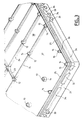
- the housing of the present invention comprises at least a base part (2) and a cover part (3) clamped together with screws or pin screws (4).
- the housing consists only of base part (2) and cover part (3).
- the assembled housing comprises one or more intermediate parts (1 ) as shown in fig. 1.
- the intermediate part (1) closest to base part (2) serves as a cover to base part (2), the second intermediate part (1) serving as a cover to the first one and so on with cover part (3) on top of the stack.
- Each part (1 - 3) is preferably machined or cast in one piece.
- Each intermediate part (1 ) and the base part (2) can accommodate one or more substrates (7) as indicated in the front view cross section in fig. 4 and the rear view cross section in fig. 5.
- a core element of the invention is the mechanical support and the thermal conductive connection provided by spacers (9 - 14) which can be part either of internal dividing walls (spacers 9, 12) or stand alone (spacers 10, 13) or be part of an outer wall (spacers 11, 14).
- spacers (9 - 14) After assembly of the housing, the spacers (9 - 14) in adjacent parts (1 - 3) touch each other with their upper and lower faces forming segments of a continuos structure.
- the spacers (9 - 11) are in immediate contact with corresponding spacers (12 - 14) on the bottom side of the adjacent part (1, 3) through recesses (28), e.g. holes, in the substrates (7). This gives a continuos vertical path with low thermal and electrical resistance.
- the resistance value can easily be adjusted by varying the diameter of the spacers (9 - 14).
- the diameter can vary locally for one or a few of the spacers (9 - 14) or for all, as required by the necessary internal heat dissipation.
- Spacers can also be formed as dividing walls (16) with a larger height which rest directly on the dividing wall (23, 24) of an adjacent part (1 - 3).
- some or all spacers have holes (15) to accommodate screws or pin screws (4) which hold the parts (1 - 3) together.
- the screws engage threads in the base part (2), or go through the complete housing into a supporting structure or panel.
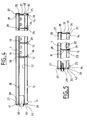
- base part (2) A cross section of base part (2) is shown in fig. 6.
- the main difference compared to an intermediate part (1 ) is that the outer wall forming the bottom (39) of base part (2) is flat.
- base part (2) is provided with means for the thermal and mechanical connection to an outside structure supporting the housing, e. g. a panel at the next integration level. Suitable connection means include mounting flanges (5) and feet (6)
- the bottom (39) serves as the main conductive thermal interface to the supporting structure or panel.
- Fig. 7 shows a cross section of cover part (3). It is also a modified version of an intermediate part (1).
- the outer wall forming the top side (40) of the housing can either be flat or have means for the mechanical, thermal or electrical connection with elements outside the housing, e.g. protrusions (8) to accommodate connectors in openings (32).
- Another element of the invention is the support of the substrates (7) inside the housing.
- the support allows for variations from production tolerances and thermal mismatch.
- Internal dividing walls (16 - 18) subdivide the inner space of the housing into compartments (38).
- the substrates (7) rest freely on the edges of the dividing walls (17, 18) and on a ledge (20) on the inside of outer wall (21).
- the dividing walls (17, 18) and the ledge (20) have the same height measured from the plane of a horizontal dividing wall (22) of an intermediate part (1) or the bottom (39) in the case of base part (2).
- the next part (1, 3) in the stack has dividing walls (23, 24) and an edge (25) of an outer wall (21) in positions which correspond to the walls (17, 18) and ledge (20).
- the edges of the dividing walls (23, 24) and the edge (25) are provided with an elastic, preferably electrically conductive gasket (26) placed in a groove.
- the gaskets (26) which are located only on one side of the substrates (7) clamp it down against the edges of the dividing walls (17, 18) and ledge (20) on the opposite side. This ensures a controlled contact pressure between the substrates (7) and their supporting structures providing both a good electrical connection for grounding and good thermal paths to the outside of the housing because the gasket (26) accommodates for production tolerances and thermal expansion mismatch in the vertical direction.
- the substrates (7) are covered with a conductive strip or a ground plane in all areas resting on the dividing walls (17, 18) and ledge (20) and preferably in the areas contacting the gaskets (26). In this way, the good electrical and thermal contact between the substrates (7) and the parts (1 - 3) of the housing is improved further.
- the walls (16 - 18, 21 - 24) also serve as thermal shunts reducing temperature differences across the substrates (7). At the same time, they thermally connect all areas of the substrates (7) to the spacers (9 - 14). Sections (19) of the dividing walls have an increased thickness in order to optimize the thermal conduction while maintaining a minimum total mass of the housing. Furthermore, the wall system also provides a shielding between the compartments (38) in the housing and ensures, together with the spacers (9 - 14), an extremely good mechanical stiffness.
- connections from the substrate to the outside of the housing or between different substrates are preferably obtained by flexible connectors (29), sliding connectors (30) or a combination of both.
- sliding connectors (30) the clearance between the outer wall (21) and the connector on the substrate (7) is normally sealed with a conductive gasket (31).
- Sliding connectors (30) are accommodated in openings (32) with an approximately trapezoidal shape while openings (33) with a round cross section accommodate flexible connectors (29).
- Variations of this basic design comprise a single or more and smaller substrates (7).
- Another possibility is to have different sizes of the compartments (38) in different parts (1 - 3) of the housing.
- the dividing walls (23, 24) in the cover part (3) are in registry with dividing walls (16 - 18) in the base part (2). If spacers are not at matching positions throughout the whole stack of parts (1 - 3), the screws through the holes (15) may stop at the respective part (1).
- a modular and strong multi-compartment housing is designed which can be optimized for minimum mass. It provides good electromagnetic shielding for the enclosed components avoiding radiation from the inside, susceptibility from electromagnetic interference and cosmic radiation. Electromagnetic shielding between components in different compartments of the housing is also possible. There is a good thermal conductive coupling to the base part from distributed areas inside the housing which allows for rapid heat conduction to underlying structures. Finally, mechanical stress caused by production tolerances or different thermal expansion between construction elements is avoided.
Landscapes
- Engineering & Computer Science (AREA)
- Microelectronics & Electronic Packaging (AREA)
- Shielding Devices Or Components To Electric Or Magnetic Fields (AREA)
- Casings For Electric Apparatus (AREA)
Applications Claiming Priority (2)
| Application Number | Priority Date | Filing Date | Title |
|---|---|---|---|
| NO986129A NO986129L (no) | 1998-12-23 | 1998-12-23 | Beskyttet modulært hus for substrat |
| NO986129 | 1998-12-23 |
Publications (3)
| Publication Number | Publication Date |
|---|---|
| EP1014770A2 true EP1014770A2 (de) | 2000-06-28 |
| EP1014770A3 EP1014770A3 (de) | 2000-11-02 |
| EP1014770B1 EP1014770B1 (de) | 2006-02-22 |
Family
ID=19902778
Family Applications (1)
| Application Number | Title | Priority Date | Filing Date |
|---|---|---|---|
| EP99403159A Expired - Lifetime EP1014770B1 (de) | 1998-12-23 | 1999-12-16 | Abgeschirmtes Modulgehäuse für Substrate |
Country Status (6)
| Country | Link |
|---|---|
| US (1) | US6327156B1 (de) |
| EP (1) | EP1014770B1 (de) |
| AT (1) | ATE318501T1 (de) |
| CA (1) | CA2291318C (de) |
| DE (1) | DE69929950D1 (de) |
| NO (1) | NO986129L (de) |
Families Citing this family (7)
| Publication number | Priority date | Publication date | Assignee | Title |
|---|---|---|---|---|
| FR2801124B1 (fr) * | 1999-11-15 | 2002-02-08 | Neopost Ind | Module de comptabilisation securise pour machine a affranchir |
| US6545870B1 (en) * | 2001-12-14 | 2003-04-08 | Hewlett-Packard Development Company, L.P. | Screwless retention of heatsink load to chassis |
| TW588897U (en) * | 2002-12-27 | 2004-05-21 | Hitron Technologies Inc | Modularized mechanism housing structure |
| US6906266B2 (en) * | 2003-03-03 | 2005-06-14 | International Business Machines Corporation | Method and structure for fastening a planar board to a chassis |
| JP4186732B2 (ja) * | 2003-07-24 | 2008-11-26 | 株式会社村田製作所 | 電子機器 |
| US20070041160A1 (en) * | 2005-08-19 | 2007-02-22 | Kehret William E | Thermal management for a ruggedized electronics enclosure |
| CN101457783B (zh) * | 2007-12-14 | 2011-07-27 | 鸿富锦精密工业(深圳)有限公司 | 锁固机构 |
Family Cites Families (12)
| Publication number | Priority date | Publication date | Assignee | Title |
|---|---|---|---|---|
| US4661888A (en) * | 1984-07-03 | 1987-04-28 | Hewlett-Packard Company | Removable modular housing for RF circuits |
| US5107404A (en) * | 1989-09-14 | 1992-04-21 | Astec International Ltd. | Circuit board assembly for a cellular telephone system or the like |
| JP2663823B2 (ja) * | 1993-01-29 | 1997-10-15 | 松下電器産業株式会社 | 高周波装置 |
| US5373104A (en) * | 1993-07-12 | 1994-12-13 | Delco Electronics Corporation | Control module with integral fastening/locking assembly |
| US5363276A (en) * | 1993-09-01 | 1994-11-08 | Ncr Corporation | Apparatus for containing and supporting electronic components |
| JPH088573A (ja) * | 1994-06-21 | 1996-01-12 | Nec Corp | シールドケース構造 |
| US5677830A (en) * | 1995-03-02 | 1997-10-14 | Mitel Corporation | Modular, stacking, expandable electronic enclosure system |
| US5550713A (en) * | 1995-09-06 | 1996-08-27 | Aironet Wireless Communications, Inc. | Electromagnetic shielding assembly for printed circuit board |
| US5777844A (en) * | 1996-08-30 | 1998-07-07 | General Electric Company | Electronic control with heat sink |
| JPH10154890A (ja) * | 1996-11-22 | 1998-06-09 | Mitsumi Electric Co Ltd | 複数のシールドケースの組立構造 |
| US5867369A (en) * | 1997-07-15 | 1999-02-02 | Sun Microsystems, Inc. | Rugged computer housing |
| US6043981A (en) * | 1997-11-13 | 2000-03-28 | Chrysler Corporation | Heat sink assembly for electrical components |
-
1998
- 1998-12-23 NO NO986129A patent/NO986129L/no unknown
-
1999
- 1999-11-30 CA CA002291318A patent/CA2291318C/en not_active Expired - Lifetime
- 1999-12-02 US US09/452,871 patent/US6327156B1/en not_active Expired - Lifetime
- 1999-12-16 DE DE69929950T patent/DE69929950D1/de not_active Expired - Lifetime
- 1999-12-16 AT AT99403159T patent/ATE318501T1/de not_active IP Right Cessation
- 1999-12-16 EP EP99403159A patent/EP1014770B1/de not_active Expired - Lifetime
Also Published As
| Publication number | Publication date |
|---|---|
| NO986129L (no) | 2000-06-26 |
| NO986129D0 (no) | 1998-12-23 |
| EP1014770B1 (de) | 2006-02-22 |
| EP1014770A3 (de) | 2000-11-02 |
| US6327156B1 (en) | 2001-12-04 |
| DE69929950D1 (de) | 2006-04-27 |
| ATE318501T1 (de) | 2006-03-15 |
| CA2291318A1 (en) | 2000-06-23 |
| CA2291318C (en) | 2007-05-29 |
Similar Documents
| Publication | Publication Date | Title |
|---|---|---|
| US6101089A (en) | Electronic apparatus | |
| US5414592A (en) | Heat transforming arrangement for printed wiring boards | |
| US5691504A (en) | Multilayer computer chassis having integral circuit board mounting and grounding structure | |
| CN102017830B (zh) | 互锁emi屏蔽物 | |
| US6222732B1 (en) | Electrical device, in particular a switching and control unit for motor vehicles | |
| JP2730984B2 (ja) | 無線周波防害遮蔽ガスケット | |
| US20060262512A1 (en) | Modular electronics enclosure | |
| US5796593A (en) | Planar mounts capable of mounting planars of varying thickness | |
| US5668509A (en) | Modified coaxial to GCPW vertical solderless interconnects for stack MIC assemblies | |
| US4316236A (en) | Hinged support for electrical devices | |
| JPH05501030A (ja) | 電気回路のための電磁シールド | |
| US20050039941A1 (en) | Device and method for clamping and grounding a cable | |
| EP1014770B1 (de) | Abgeschirmtes Modulgehäuse für Substrate | |
| JPH0267797A (ja) | 無線周波妨害遮蔽装置 | |
| WO1998006146A1 (en) | Transmit/receive antenna mounting enclosure | |
| US4864077A (en) | Shielded enclosure | |
| US5604668A (en) | Apparatus for shielding electronic circuit boards | |
| US8050039B2 (en) | Portable environmentally robust enclosure optimized for size, weight, and power dissipation | |
| US6200142B1 (en) | Assembly including a flex circuit and a gas tight chamber | |
| US6088227A (en) | Heat sink with integrated buss bar | |
| US20240098885A1 (en) | Rf connector and communication apparatus including same | |
| CN110610666A (zh) | 柔性显示屏安装装置和显示装置 | |
| EP3579218B1 (de) | Anzeigevorrichtungssteuerungseinheit und anzeigevorrichtung | |
| EP4622019A1 (de) | Hf-verbinder und kommunikationsvorrichtung damit | |
| JPH08102592A (ja) | 実装基板用電磁シールドケース |
Legal Events
| Date | Code | Title | Description |
|---|---|---|---|
| PUAI | Public reference made under article 153(3) epc to a published international application that has entered the european phase |
Free format text: ORIGINAL CODE: 0009012 |
|
| AK | Designated contracting states |
Kind code of ref document: A2 Designated state(s): AT BE CH CY DE DK ES FI FR GB GR IE IT LI LU MC NL PT SE |
|
| AX | Request for extension of the european patent |
Free format text: AL;LT;LV;MK;RO;SI |
|
| PUAL | Search report despatched |
Free format text: ORIGINAL CODE: 0009013 |
|
| AK | Designated contracting states |
Kind code of ref document: A3 Designated state(s): AT BE CH CY DE DK ES FI FR GB GR IE IT LI LU MC NL PT SE |
|
| AX | Request for extension of the european patent |
Free format text: AL;LT;LV;MK;RO;SI |
|
| RIC1 | Information provided on ipc code assigned before grant |
Free format text: 7H 05K 5/00 A, 7H 05K 9/00 B, 7H 05K 7/14 B |
|
| 17P | Request for examination filed |
Effective date: 20010502 |
|
| AKX | Designation fees paid |
Free format text: AT BE CH CY DE DK ES FI FR GB GR IE IT LI LU MC NL PT SE |
|
| GRAP | Despatch of communication of intention to grant a patent |
Free format text: ORIGINAL CODE: EPIDOSNIGR1 |
|
| RAP1 | Party data changed (applicant data changed or rights of an application transferred) |
Owner name: NORSPACE AS |
|
| GRAS | Grant fee paid |
Free format text: ORIGINAL CODE: EPIDOSNIGR3 |
|
| GRAA | (expected) grant |
Free format text: ORIGINAL CODE: 0009210 |
|
| AK | Designated contracting states |
Kind code of ref document: B1 Designated state(s): AT BE CH CY DE DK ES FI FR GB GR IE IT LI LU MC NL PT SE |
|
| PG25 | Lapsed in a contracting state [announced via postgrant information from national office to epo] |
Ref country code: NL Free format text: LAPSE BECAUSE OF FAILURE TO SUBMIT A TRANSLATION OF THE DESCRIPTION OR TO PAY THE FEE WITHIN THE PRESCRIBED TIME-LIMIT Effective date: 20060222 Ref country code: LI Free format text: LAPSE BECAUSE OF FAILURE TO SUBMIT A TRANSLATION OF THE DESCRIPTION OR TO PAY THE FEE WITHIN THE PRESCRIBED TIME-LIMIT Effective date: 20060222 Ref country code: IT Free format text: LAPSE BECAUSE OF FAILURE TO SUBMIT A TRANSLATION OF THE DESCRIPTION OR TO PAY THE FEE WITHIN THE PRE;WARNING: LAPSES OF ITALIAN PATENTS WITH EFFECTIVE DATE BEFORE 2007 MAY HAVE OCCURRED AT ANY TIME BEFORE 2007. THE CORRECT EFFECTIVE DATE MAY BE DIFFERENT FROM THE ONE RECORDED.SCRIBED TIME-LIMIT Effective date: 20060222 Ref country code: FI Free format text: LAPSE BECAUSE OF FAILURE TO SUBMIT A TRANSLATION OF THE DESCRIPTION OR TO PAY THE FEE WITHIN THE PRESCRIBED TIME-LIMIT Effective date: 20060222 Ref country code: CH Free format text: LAPSE BECAUSE OF FAILURE TO SUBMIT A TRANSLATION OF THE DESCRIPTION OR TO PAY THE FEE WITHIN THE PRESCRIBED TIME-LIMIT Effective date: 20060222 Ref country code: BE Free format text: LAPSE BECAUSE OF FAILURE TO SUBMIT A TRANSLATION OF THE DESCRIPTION OR TO PAY THE FEE WITHIN THE PRESCRIBED TIME-LIMIT Effective date: 20060222 Ref country code: AT Free format text: LAPSE BECAUSE OF FAILURE TO SUBMIT A TRANSLATION OF THE DESCRIPTION OR TO PAY THE FEE WITHIN THE PRESCRIBED TIME-LIMIT Effective date: 20060222 |
|
| REG | Reference to a national code |
Ref country code: GB Ref legal event code: FG4D |
|
| REG | Reference to a national code |
Ref country code: CH Ref legal event code: EP |
|
| REG | Reference to a national code |
Ref country code: IE Ref legal event code: FG4D |
|
| REF | Corresponds to: |
Ref document number: 69929950 Country of ref document: DE Date of ref document: 20060427 Kind code of ref document: P |
|
| PG25 | Lapsed in a contracting state [announced via postgrant information from national office to epo] |
Ref country code: SE Free format text: LAPSE BECAUSE OF FAILURE TO SUBMIT A TRANSLATION OF THE DESCRIPTION OR TO PAY THE FEE WITHIN THE PRESCRIBED TIME-LIMIT Effective date: 20060522 Ref country code: DK Free format text: LAPSE BECAUSE OF FAILURE TO SUBMIT A TRANSLATION OF THE DESCRIPTION OR TO PAY THE FEE WITHIN THE PRESCRIBED TIME-LIMIT Effective date: 20060522 |
|
| PG25 | Lapsed in a contracting state [announced via postgrant information from national office to epo] |
Ref country code: DE Free format text: LAPSE BECAUSE OF FAILURE TO SUBMIT A TRANSLATION OF THE DESCRIPTION OR TO PAY THE FEE WITHIN THE PRESCRIBED TIME-LIMIT Effective date: 20060523 |
|
| PG25 | Lapsed in a contracting state [announced via postgrant information from national office to epo] |
Ref country code: ES Free format text: LAPSE BECAUSE OF FAILURE TO SUBMIT A TRANSLATION OF THE DESCRIPTION OR TO PAY THE FEE WITHIN THE PRESCRIBED TIME-LIMIT Effective date: 20060602 |
|
| PG25 | Lapsed in a contracting state [announced via postgrant information from national office to epo] |
Ref country code: PT Free format text: LAPSE BECAUSE OF FAILURE TO SUBMIT A TRANSLATION OF THE DESCRIPTION OR TO PAY THE FEE WITHIN THE PRESCRIBED TIME-LIMIT Effective date: 20060724 |
|
| NLV1 | Nl: lapsed or annulled due to failure to fulfill the requirements of art. 29p and 29m of the patents act | ||
| REG | Reference to a national code |
Ref country code: CH Ref legal event code: PL |
|
| ET | Fr: translation filed | ||
| PG25 | Lapsed in a contracting state [announced via postgrant information from national office to epo] |
Ref country code: IE Free format text: LAPSE BECAUSE OF NON-PAYMENT OF DUE FEES Effective date: 20061218 |
|
| PLBE | No opposition filed within time limit |
Free format text: ORIGINAL CODE: 0009261 |
|
| STAA | Information on the status of an ep patent application or granted ep patent |
Free format text: STATUS: NO OPPOSITION FILED WITHIN TIME LIMIT |
|
| PG25 | Lapsed in a contracting state [announced via postgrant information from national office to epo] |
Ref country code: MC Free format text: LAPSE BECAUSE OF NON-PAYMENT OF DUE FEES Effective date: 20061231 |
|
| 26N | No opposition filed |
Effective date: 20061123 |
|
| PG25 | Lapsed in a contracting state [announced via postgrant information from national office to epo] |
Ref country code: GR Free format text: LAPSE BECAUSE OF FAILURE TO SUBMIT A TRANSLATION OF THE DESCRIPTION OR TO PAY THE FEE WITHIN THE PRESCRIBED TIME-LIMIT Effective date: 20060523 |
|
| PG25 | Lapsed in a contracting state [announced via postgrant information from national office to epo] |
Ref country code: LU Free format text: LAPSE BECAUSE OF NON-PAYMENT OF DUE FEES Effective date: 20061216 |
|
| PG25 | Lapsed in a contracting state [announced via postgrant information from national office to epo] |
Ref country code: CY Free format text: LAPSE BECAUSE OF FAILURE TO SUBMIT A TRANSLATION OF THE DESCRIPTION OR TO PAY THE FEE WITHIN THE PRESCRIBED TIME-LIMIT Effective date: 20060222 |
|
| REG | Reference to a national code |
Ref country code: FR Ref legal event code: PLFP Year of fee payment: 17 |
|
| REG | Reference to a national code |
Ref country code: FR Ref legal event code: PLFP Year of fee payment: 18 |
|
| REG | Reference to a national code |
Ref country code: FR Ref legal event code: PLFP Year of fee payment: 19 |
|
| PGFP | Annual fee paid to national office [announced via postgrant information from national office to epo] |
Ref country code: GB Payment date: 20181218 Year of fee payment: 20 Ref country code: FR Payment date: 20181219 Year of fee payment: 20 |
|
| REG | Reference to a national code |
Ref country code: GB Ref legal event code: PE20 Expiry date: 20191215 |
|
| PG25 | Lapsed in a contracting state [announced via postgrant information from national office to epo] |
Ref country code: GB Free format text: LAPSE BECAUSE OF EXPIRATION OF PROTECTION Effective date: 20191215 |