EP1016893A1 - Afficheur a cristaux liquides insensible aux taches - Google Patents
Afficheur a cristaux liquides insensible aux taches Download PDFInfo
- Publication number
- EP1016893A1 EP1016893A1 EP98905714A EP98905714A EP1016893A1 EP 1016893 A1 EP1016893 A1 EP 1016893A1 EP 98905714 A EP98905714 A EP 98905714A EP 98905714 A EP98905714 A EP 98905714A EP 1016893 A1 EP1016893 A1 EP 1016893A1
- Authority
- EP
- European Patent Office
- Prior art keywords
- liquid crystal
- display device
- crystal display
- layer
- surface protective
- Prior art date
- Legal status (The legal status is an assumption and is not a legal conclusion. Google has not performed a legal analysis and makes no representation as to the accuracy of the status listed.)
- Withdrawn
Links
Images
Classifications
-
- G—PHYSICS
- G02—OPTICS
- G02F—OPTICAL DEVICES OR ARRANGEMENTS FOR THE CONTROL OF LIGHT BY MODIFICATION OF THE OPTICAL PROPERTIES OF THE MEDIA OF THE ELEMENTS INVOLVED THEREIN; NON-LINEAR OPTICS; FREQUENCY-CHANGING OF LIGHT; OPTICAL LOGIC ELEMENTS; OPTICAL ANALOGUE/DIGITAL CONVERTERS
- G02F1/00—Devices or arrangements for the control of the intensity, colour, phase, polarisation or direction of light arriving from an independent light source, e.g. switching, gating or modulating; Non-linear optics
- G02F1/01—Devices or arrangements for the control of the intensity, colour, phase, polarisation or direction of light arriving from an independent light source, e.g. switching, gating or modulating; Non-linear optics for the control of the intensity, phase, polarisation or colour
- G02F1/13—Devices or arrangements for the control of the intensity, colour, phase, polarisation or direction of light arriving from an independent light source, e.g. switching, gating or modulating; Non-linear optics for the control of the intensity, phase, polarisation or colour based on liquid crystals, e.g. single liquid crystal display cells
- G02F1/133—Constructional arrangements; Operation of liquid crystal cells; Circuit arrangements
- G02F1/1333—Constructional arrangements; Manufacturing methods
- G02F1/1334—Constructional arrangements; Manufacturing methods based on polymer dispersed liquid crystals, e.g. microencapsulated liquid crystals
-
- G—PHYSICS
- G02—OPTICS
- G02F—OPTICAL DEVICES OR ARRANGEMENTS FOR THE CONTROL OF LIGHT BY MODIFICATION OF THE OPTICAL PROPERTIES OF THE MEDIA OF THE ELEMENTS INVOLVED THEREIN; NON-LINEAR OPTICS; FREQUENCY-CHANGING OF LIGHT; OPTICAL LOGIC ELEMENTS; OPTICAL ANALOGUE/DIGITAL CONVERTERS
- G02F1/00—Devices or arrangements for the control of the intensity, colour, phase, polarisation or direction of light arriving from an independent light source, e.g. switching, gating or modulating; Non-linear optics
- G02F1/01—Devices or arrangements for the control of the intensity, colour, phase, polarisation or direction of light arriving from an independent light source, e.g. switching, gating or modulating; Non-linear optics for the control of the intensity, phase, polarisation or colour
- G02F1/13—Devices or arrangements for the control of the intensity, colour, phase, polarisation or direction of light arriving from an independent light source, e.g. switching, gating or modulating; Non-linear optics for the control of the intensity, phase, polarisation or colour based on liquid crystals, e.g. single liquid crystal display cells
- G02F1/133—Constructional arrangements; Operation of liquid crystal cells; Circuit arrangements
- G02F1/1333—Constructional arrangements; Manufacturing methods
-
- G—PHYSICS
- G02—OPTICS
- G02F—OPTICAL DEVICES OR ARRANGEMENTS FOR THE CONTROL OF LIGHT BY MODIFICATION OF THE OPTICAL PROPERTIES OF THE MEDIA OF THE ELEMENTS INVOLVED THEREIN; NON-LINEAR OPTICS; FREQUENCY-CHANGING OF LIGHT; OPTICAL LOGIC ELEMENTS; OPTICAL ANALOGUE/DIGITAL CONVERTERS
- G02F1/00—Devices or arrangements for the control of the intensity, colour, phase, polarisation or direction of light arriving from an independent light source, e.g. switching, gating or modulating; Non-linear optics
- G02F1/01—Devices or arrangements for the control of the intensity, colour, phase, polarisation or direction of light arriving from an independent light source, e.g. switching, gating or modulating; Non-linear optics for the control of the intensity, phase, polarisation or colour
- G02F1/13—Devices or arrangements for the control of the intensity, colour, phase, polarisation or direction of light arriving from an independent light source, e.g. switching, gating or modulating; Non-linear optics for the control of the intensity, phase, polarisation or colour based on liquid crystals, e.g. single liquid crystal display cells
- G02F1/137—Devices or arrangements for the control of the intensity, colour, phase, polarisation or direction of light arriving from an independent light source, e.g. switching, gating or modulating; Non-linear optics for the control of the intensity, phase, polarisation or colour based on liquid crystals, e.g. single liquid crystal display cells characterised by the electro-optical or magneto-optical effect, e.g. field-induced phase transition, orientation effect, guest-host interaction or dynamic scattering
- G02F1/139—Devices or arrangements for the control of the intensity, colour, phase, polarisation or direction of light arriving from an independent light source, e.g. switching, gating or modulating; Non-linear optics for the control of the intensity, phase, polarisation or colour based on liquid crystals, e.g. single liquid crystal display cells characterised by the electro-optical or magneto-optical effect, e.g. field-induced phase transition, orientation effect, guest-host interaction or dynamic scattering based on orientation effects in which the liquid crystal remains transparent
- G02F1/1396—Devices or arrangements for the control of the intensity, colour, phase, polarisation or direction of light arriving from an independent light source, e.g. switching, gating or modulating; Non-linear optics for the control of the intensity, phase, polarisation or colour based on liquid crystals, e.g. single liquid crystal display cells characterised by the electro-optical or magneto-optical effect, e.g. field-induced phase transition, orientation effect, guest-host interaction or dynamic scattering based on orientation effects in which the liquid crystal remains transparent the liquid crystal being selectively controlled between a twisted state and a non-twisted state, e.g. TN-LC cell
-
- B—PERFORMING OPERATIONS; TRANSPORTING
- B32—LAYERED PRODUCTS
- B32B—LAYERED PRODUCTS, i.e. PRODUCTS BUILT-UP OF STRATA OF FLAT OR NON-FLAT, e.g. CELLULAR OR HONEYCOMB, FORM
- B32B2457/00—Electrical equipment
- B32B2457/20—Displays, e.g. liquid crystal displays, plasma displays
- B32B2457/202—LCD, i.e. liquid crystal displays
Definitions
- the present invention relates to a liquid crystal display device, more specifically to a liquid crystal display device having an antifouling ability.
- a transparent insulator layer is provided on a liquid crystal-dispersed polymer layer in which liquid crystal is finely dispersed in a polymer matrix, so that the liquid crystal-dispersed polymer layer can be prevented from being scratched.
- the surface of the transparent insulator layer is not subjected to antifouling treatment, and therefore while contacting a conductive member with the surface of the display device to apply an electric field to the liquid crystal display device, the surface of the display device is fouled by a conductive component (for example, conductive carbon black and the like) contained in the conductive member, so that the problems that the contour of a displayed image or written lines becomes indistinct and the memory performance is reduced are caused in some cases.
- a conductive component for example, conductive carbon black and the like
- a handwriting liquid crystal board set disclosed in Japanese Patent Application Laid-Open No. Hei 5-281530 is subjected to antifouling treatment in which a writing member or an erasing member is impregnated with oil such as an insulating oil, a silicone oil and a fluorine-containing oil or covered with a polymer film, and therefore the problems described above are solved for the present.
- writing and erasing can be carried out without using a writing member and an erasing member.
- writing and erasing can be carried out as well directly by using fingers.
- the present invention has been made in order to solve the conventional problems described above, and an object thereof is to provide a liquid crystal display device having an antifouling ability in which moisture is hard to stick on the display screen and fouling matters such as sebum and sweat on a hand are hard to stick to the display screen as well in repeated use or even if writing and erasing are repeated on the display screen directly with fingers and in which even if fouling matters stick, they can easily be removed by dry wiping or wet wiping and even if the surface of the display device screen is scratched by repeated use, moisture is hard to stick.
- the liquid crystal display device having an antifouling ability of the present invention is characterized by comprising at least a liquid crystal-dispersed polymer layer in which liquid crystal is finely dispersed in a polymer matrix and a surface protective layer, each of which is laminated in order on a conductive layer, wherein said surface protective layer has a contact angle of 80° or more to water and a volume resistivity of 10 13 ⁇ cm or more at a temperature of 20°C and a relative humidity of 90%.
- the preferred liquid crystal display device of the present invention comprises mainly a transparent high electric resistance layer having a volume resistivity of 10 13 ⁇ cm or more at a temperature of 20°C and a relative humidity of 90 %.
- the conductive layer of the liquid crystal display device may be either transparent or opaque and may be any layer as long as it has a surface resistance of 10 7 ⁇ / ⁇ or less. Practically, the layer is obtained by providing the surface of a substrate with conductivity by aluminum, titanium, chromium, tin, rhodium, gold, stainless steel, titanium nitride, nickel-chromium, aluminum-chromium or indium tin oxide.
- the substrate described above is intended to hold the conductive layer and includes, to be specific, paper, cloth, non-woven fabric, and plastic films of polyethylene terephthalate, polyethylene naphthalate, polypropylene, polyethylene, polyvinyl chloride, polysulfone, polyphenylene oxide, ionomer, polyimide and polycarbonate and the like.
- plastic films of polyethylene terephthalate, polyethylene naphthalate, polypropylene, polyethylene, polyvinyl chloride, polysulfone, polyphenylene oxide, ionomer, polyimide and polycarbonate and the like.
- the conductive layer itself is a metal film, such a substrate is not specifically required.
- the liquid crystal-dispersed polymer layer of the liquid crystal display device is obtained by dispersing liquid crystal in a polymer matrix.
- a process for dispersing liquid crystal in a polymer matrix includes a phase separation process of evaporating a common solvent for a polymer/liquid crystal (common solvent casting process), a polymerization phase separation process in which a polymer precursor in a liquid crystal/polymer precursor mixture is polymerized by light or heat, a melting/cooling phase separation process in which liquid crystal and a polymer are cooled from a heated and molten state and a process in which liquid crystal that is emulsion-dispersed in an aqueous resin is applied and dried to disperse in a polymer matrix, and they can suitably be used.
- the polymer capable of being used for this liquid crystal-dispersed polymer layer may be any one as long as it is a polymer which is hard to be miscible with the liquid crystal, and to be specific, it includes vinyl resins such as chlorinated polyethylene, polystyrene and acryl resins, vinylidene chloride resins, polyvinyl acetal resins, cellulose resins, ionomers, polyamide, polycarbonate, styrene-butadiene rubber, chlorosulfonated polyethylene, polyester and epoxy resins.
- the polyvinyl acetal resins include polyvinyl formal, polyvinyl acetal and polyvinyl butyral and the like.
- cross-linked polymer polymers having cross-linking structure
- the cross-linked polymer is not miscrible at all with the liquid crystal even when the liquid crystal display device of the present invention is left in a high temperature state, and the stable liquid crystal-finely dispersed structure can be maintained. This makes it possible to obtain a liquid crystal sheet having durability in which performances are not deteriorated with the passage of time.
- the cross-linked polymer includes, for example, cross-linked polymers obtained by mixing and reacting polymers having functional groups such as a double bond, hydroxy, carboxy, epoxy, isocyanate, amino and chlorosulfone with cross-linking agents which react with functional groups and cross-linked polymers obtained by mixing and reacting polymers having the functional groups described above with reactive polymers.
- cross-linking agents used for the reaction described above include isocyanate compounds, organic peroxides, amine compounds, epoxy compounds, dicarboxylic acids or carboxylic anhydrides, formaldehyde, dialdehydes, diols, bisphenols and photo cross-linking agents (photo polymerization initiators), and the reactive polymers include phenol resins, amino resins, polyols and epoxy resins.
- the preferred cross-linked polymer includes cross-linked polymers obtained by reacting di- or polyisocyanates with polymers such as polyvinyl acetal resins, epoxy resins, acryl resins having functional groups such as a hydroxy group and a carboxy group, and polyester resins. More preferred cross-linked polymers are cross-linked polymers obtained by reacting di- or polyisocyanates with polyvinyl acetal resins.
- the polyvinyl acetal resins are polyvinyl formal, polyvinyl acetal, polyvinyl butyral and the like.
- the liquid crystal used for the liquid crystal-dispersed polymer layer is preferably nematic liquid crystal having a positive dielectric anisotropy.
- the liquid crystal phase has preferably a temperature range of -10 to 100°C in terms of practical use and a birefringence index ⁇ n of 0.2 or more in order to display vividly the recorded image.
- the liquid crystal-dispersed polymer layer of the liquid crystal display device has preferably a volume resistivity of 10 13 ⁇ cm or more at a temperature of 20°C and a relative humidity of 90 % (hereinafter abbreviated as 90 % RH).
- 90 % RH a volume resistivity of 10 13 ⁇ cm or more at a temperature of 20°C and a relative humidity of 90 %
- applied static charge becomes hard to move and attenuate in the direction of the front and back of the display screen, and therefore the erasability goes up as well.
- applied static charge is easy to move and attenuate on the surface and in the direction of the front and back of the display screen, and therefore the static charge disappears and attenuates as time passes, so that the static charge becomes imbalanced on the surface and in the direction of the front and back of the display screen.
- the contour of the recorded image, the memory performance and the erasability are deteriorated.
- the surface protective layer of the liquid crystal display device is composed of a transparent and water-repellent polymer having a high electric resistance. That is, the surface protective layer has a contact angle of 80° or more to water and a volume resistivity of 10 13 ⁇ cm or more at a temperature of 20°C and 90 % RH. If the surface protective layer has a contact angle of less than 80° to water, it can not have a satisfactory water-repellence, and moisture and fouling matters such as sebum and sweat on a hand and cosmetics are liable to stick on the surface of the display device screen.
- the surface protective layer has a contact angle of 80° or more to water, moisture and fouling matters can easily be removed by dry wiping or wet wiping even if they stick on the surface of the display device screen. Further, even if the surface of the display device screen is scratched by repeated use, it does not become hydrophilic, and moisture is hard to stick on the surface even under an environment of high humidity. If the surface protective layer having a volume resistivity of less than 10 13 ⁇ cm at a temperature of 20°C and 90 % RH is used, problems on the performances are caused for the same reasons as in the case of the liquid crystal-dispersed polymer layer described above, and the practical liquid crystal display device is not obtained.
- Materials constituting the surface protective layer include, for example, silicone resins, thermosetting silicone resins, photosetting silicone resins, fluororesin, thermosetting fluororesins, photosetting fluororesins, and polymers containing a silicone or fluorine component at a principal chain part, a side chain part or a terminal part.
- the surface protective layer is obtained by laminating a film comprising the materials described above with a bond or adhesive, applying and drying a solution of a material having the physical properties described above or applying a solution of a reactive material and then reacting it.
- a transparent high electric resistance layer is preferably provided between the conductive layer and the liquid crystal-dispersed polymer layer, and the volume resistivity thereof is preferably 10 13 ⁇ cm or more at a temperature of 20°C and 90 % RH. Because of the surer prevention of movement and attenuation of static charge applied on the display device screen, this transparent high electric resistance layer improves the performances such as the vividness of the contour of the recorded image, the memory performance and the erasability. If the layer having a volume resistivity of less than 10 13 ⁇ cm at a temperature of 20°C and 90 % RH is used, problems on the performances are caused for the same reasons as in the case of the liquid crystal-dispersed polymer layer described above, and such a layer is not practical.
- Polymers used for the transparent high electric resistance layer include vinyl resins such as chlorinated polyethylene, polystyrene and acryl resins, vinylidene chloride resins, polyvinyl acetal resins, cellulose resins, ionomers, polyamide, polycarbonate, styrenebutadiene rubber, chlorosulfonated polyethylene. polyester and epoxy resins.
- the polyvinyl acetal resins are polyvinyl formal, polyvinyl acetal, polyvinyl butyral and the like.
- cross-linked polymers can also be used as the polymer for the transparent high electric resistance layer. They include, for example, cross-linked polymers obtained by mixing and reacting polymers having functional groups such as a double bond, hydroxy, carboxy, epoxy, isocyanate, amino and chlorosulfone with cross-linking agents which react with functional groups and cross-linked polymers obtained by mixing and reacting polymers having the functional groups described above with reactive polymers.
- cross-linking agents used for the reaction described above include isocyanate compounds, organic peroxides, amine compounds, epoxy compounds, dicarboxylic acid or carboxylic anhydrides, formaldehyde, dialdehydes, diols, bisphenols and photo cross-linking agents (photo polymerization initiators), and the reactive polymers include phenol resins, amino resins, polyols and epoxy resins.
- the preferred cross-linked polymer includes cross-linked polymers obtained by reacting di- or polyisocyanates with polymers such as polyvinyl acetal resins, epoxy resins, acryl resins having functional groups such as a hydroxy group and a carboxy group and polyester resins. More preferred cross-linked polymers are cross-linked polymers obtained by reacting di- or polyisocyanates with polyvinyl acetal resins.
- the polyvinyl acetal resins are polyvinyl formal, polyvinyl acetal, polyvinyl butyral and the like.
- the transparent high electric resistance layer can be obtained by applying a solution of a material for the layer or applying and reacting a solution of a reactive material. Or, it can be obtained as well by laminating a film having a high electric resistance with a bond or adhesive.
- the transparent high electric resistance layer has a thickness falling suitably in a range of 0.4 to 10 ⁇ m.
- the reactive materials there are combinations of, for example, a di- or polyisocyanate compound for the cross-linking agent with polyvinyl alkylal, an epoxy resin, a carboxyl group-containing acryl resin or a polyester resin for the compound reacting with the above cross-linking agent.
- the films having a high electric resistance include films of polyethylene terephthalate, polyethylene naphthalate, polypropylene, polyethylene, polyvinyl chloride, polysulfone, polyphenylene oxide, ionomer and polycarbonate.
- a solution comprising the following components was applied as a liquid crystal-dispersed polymer layer 2 on a conductive layer 6 which was an aluminum-deposited layer (#125 METALLUMY TS; aluminum-deposited film which uses a polyethylene terephthalate film as a substrate 7: manufactured by TOYO METALLIZING Co., Ltd.) so that the dried film thickness thereof was 7 ⁇ m, and then it was dried and cured: 10 % solution of S-LECK KS-1 (polyvinyl acetal resin: manufactured by Sekisui Chemical Co., Ltd.) in ethyl acetate 2.1 g TAKENATE D110N (polyisocyanate: manufactured by Takeda Chemical Industries, Ltd.) 0.42 g E44 (nematic liquid crystal: manufactured Merck AG.) 0.23 g
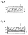
- a solution comprising the following components was applied as a surface protective layer 1 on the coated film described above so that the dried film thickness thereof was 3 ⁇ m, and then it was dried and cured to prepare the liquid crystal display device of the present example as shown in Fig. 1: Cimac US-380 (acryl ⁇ silicone coating agent: manufactured by Toagosei Co., Ltd.) 4.0 g CORONATE HX (polyisocyanate: manufactured by Nippon Polyurethane Industry Co., Ltd.) 0.27 g
- a solution comprising the following components was applied as a transparent high electric resistance layer 5 on a conductive layer 6 which was an aluminum-deposited layer (#125 METALLUMY TS; aluminum-deposited film which uses a polyethylene terephthalate film as a substrate 7: manufactured by TOYO METALLIZING Co., Ltd.) so that the dried film thickness thereof was 2.5 ⁇ m, and then it was dried and cured: 10 % solution of S-LECK KS-1 (polyvinyl acetal resin: manufactured by Sekisui Chemical Co., Ltd.) in ethyl acetate 9.0 g TAKENATE D110N (polyisocyanate: manufactured by Takeda Chemical Industries, Ltd.) 0.4 g
- a solution comprising the following components was applied as a liquid crystal-dispersed polymer layer 2 on the coated film described above so that the dried film thickness thereof was 7 ⁇ m, and then it was dried and cured: 10 % solution of S-LECK KS-1 (polyvinyl acetal resin: manufactured by Sekisui Chemical Co., Ltd.) in ethyl acetate 2.1 g TAKENATE D110N (polyisocyanate: manufactured by Takeda Chemical Industries, Ltd.) 0.42 g E44 (nematic liquid crystal: manufactured Merck AG.) 0.23 g
- a solution comprising the following components was applied as a surface protective layer 1 on the coated film described above so that the dried film thickness thereof was 3 ⁇ m, and then it was dried and cured to prepare the liquid crystal display device of the present example as shown in Fig. 2: Cimac US-380 (acryl ⁇ silicone coating agent: manufactured by Toagosei Co., Ltd.) 4.0 g CORONATE HX (polyisocyanate: manufactured by Nippon Polyurethane Industry Co., Ltd.) 0.27 g
- a conductive layer 6, a transparent high electric resistance layer 5 and a liquid crystal-dispersed polymer layer 2 were formed in the same manner as in Example 2. Further, a solution comprising the following components was applied thereon as a surface protective layer 1 so that the dried film thickness thereof was 3 ⁇ m, and then it was dried and cured to prepare the liquid crystal display device of the present example: X-22-8004 (silicone based film-forming agent: manufactured by Shin-etsu Chemical Co., Ltd.) 4.0 g TAKENATE D110N (polyisocyanate: manufactured by Takeda Chemical Industries, Ltd.) 0.18 g
- a conductive layer 6, a transparent high electric resistance layer 5 and a liquid crystal-dispersed polymer layer 2 were formed in the same manner as in Example 2. Further, a solution comprising the following components was applied thereon as a surface protective layer 1 so that the dried film thickness thereof was 3 ⁇ m, and then it was dried and cured to prepare the liquid crystal display device of the present example: Sefral Coat A-201TB (solvent-soluble type fluororesin for paint: manufactured by Central Glass Co., Ltd.) 4.0 g CORONATE HX (polyisocyanate: manufactured by Nippon Polyurethane Industry Co., Ltd.) 0.34 g
- a conductive layer 6, a transparent high electric resistance layer 5 and a liquid crystal-dispersed polymer layer 2 were formed in the same manner as in Example 2. Further, Tetoron Film F (polyethylene terephthalate film: manufactured by Teijin, Ltd.) of 9 ⁇ m was laminated thereon as a surface protective layer 1 with an adhesive to prepare a liquid crystal display device of the present comparative example.
- Tetoron Film F polyethylene terephthalate film: manufactured by Teijin, Ltd.
- a conductive layer 6, a transparent high electric resistance layer 5 and a liquid crystal-dispersed polymer layer 2 were formed in the same manner as in Example 2. Further, Tedler Film TTR05SG2 (polyvinyl fluoride film: manufactured by Du Pont Co., Ltd.) of 12 ⁇ m was laminated thereon as a surface protective layer 1 with an adhesive to prepare a liquid crystal display device of the present comparative example.
- Tedler Film TTR05SG2 polyvinyl fluoride film: manufactured by Du Pont Co., Ltd.
- a conductive layer 6, a transparent high electric resistance layer 5 and a liquid crystal-dispersed polymer layer 2 were formed in the same manner as in Example 2. Further, an aqueous solution of GF-256 (polysiloxane graft polymer dispersion in water: manufactured by Nippon Shokubai Co., Ltd.) was applied thereon as a surface protective layer 1 so that the dried film thickness thereof was 3 ⁇ m, and then it was dried to prepare a liquid crystal display device of the present comparative example.
- GF-256 polysiloxane graft polymer dispersion in water: manufactured by Nippon Shokubai Co., Ltd.
- liquid crystal display devices prepared in the examples and the comparative examples described above were evaluated for the following items.
- the volume resistivities of the respective surface protective layers which was conditioned to a relative humidity of 90 % at 20°C were determined by means of a digital ULTRA-HIGH RESISTANCE METER (R8340A: manufactured by Advantest Corp.) and an insulation resistance measuring specimen chamber (TR42: manufactured by Advantest Corp.).
- a voltage of 300 V was applied on the respective liquid crystal display devices which was conditioned to 90 % RH at 20°C from a DC power source to display images, and then they were left standing under conditions of 20°C and 90 % RH. Then, a density difference between the image part and the non-image part was determined by means of a reflection density-meter (RD-915 type: manufactured by Macbeth Co., Ltd.) to evaluate a holding time of the image.
- RD-915 type manufactured by Macbeth Co., Ltd.
- the liquid crystal display device of the present invention having an antifouling ability has a high water repellency of a surface protective layer, so that moisture and fouling matters are hard to stick on the surface of the display device even under a high humidity environment, and the contour of the written image does not become indistinct.
- the surface protective layer has a high volume resistivity, it plays a part as a conventional transparent insulator layer as well as a conventional transparent insulator layer and antifouling layer. Accordingly, the structure of the liquid crystal display device can be simplified, and the whole thickness of the element can be reduced, so that an image can be displayed at a lower voltage than ever.
- the liquid crystal display device of the present invention can be applied to a hand-writable liquid crystal board set, and even if repeatedly used or repeatedly written and erased on the display screen directly with fingers, the display screen is hard to be fouled.
- the contour of the displayed image and the memory performance for the image are held for a long period of time, and the added value as a hand-writable liquid crystal board set can be elevated.
Landscapes
- Physics & Mathematics (AREA)
- Nonlinear Science (AREA)
- Chemical & Material Sciences (AREA)
- Crystallography & Structural Chemistry (AREA)
- General Physics & Mathematics (AREA)
- Optics & Photonics (AREA)
- Mathematical Physics (AREA)
- Dispersion Chemistry (AREA)
- Liquid Crystal (AREA)
- Liquid Crystal Substances (AREA)
- Devices For Indicating Variable Information By Combining Individual Elements (AREA)
Applications Claiming Priority (3)
| Application Number | Priority Date | Filing Date | Title |
|---|---|---|---|
| JP9048841A JPH10246883A (ja) | 1997-03-04 | 1997-03-04 | 防汚性を有する液晶表示素子 |
| JP4884197 | 1997-03-04 | ||
| PCT/JP1998/000843 WO1998039683A1 (fr) | 1997-03-04 | 1998-03-02 | Afficheur a cristaux liquides insensible aux taches |
Publications (1)
| Publication Number | Publication Date |
|---|---|
| EP1016893A1 true EP1016893A1 (fr) | 2000-07-05 |
Family
ID=12814485
Family Applications (1)
| Application Number | Title | Priority Date | Filing Date |
|---|---|---|---|
| EP98905714A Withdrawn EP1016893A1 (fr) | 1997-03-04 | 1998-03-02 | Afficheur a cristaux liquides insensible aux taches |
Country Status (5)
| Country | Link |
|---|---|
| EP (1) | EP1016893A1 (fr) |
| JP (1) | JPH10246883A (fr) |
| KR (1) | KR20000075795A (fr) |
| CN (1) | CN1253634A (fr) |
| WO (1) | WO1998039683A1 (fr) |
Cited By (3)
| Publication number | Priority date | Publication date | Assignee | Title |
|---|---|---|---|---|
| US8003200B2 (en) | 2004-10-06 | 2011-08-23 | Nitto Denko Corporation | Transparent electrically-conductive film |
| US8048512B2 (en) | 2006-08-03 | 2011-11-01 | Nitto Denko Corporation | Transparent conductive laminate and touch panel equipped with it |
| US20230080269A1 (en) * | 2020-03-03 | 2023-03-16 | Sabic Global Technologies B.V. | Polypropylene film with increased hydrophobicity |
Families Citing this family (2)
| Publication number | Priority date | Publication date | Assignee | Title |
|---|---|---|---|---|
| CN103869887B (zh) * | 2012-12-18 | 2017-11-17 | 原相科技股份有限公司 | 可携的交互式电子装置 |
| CN111736377B (zh) * | 2020-06-17 | 2022-04-26 | 深圳市华星光电半导体显示技术有限公司 | 液晶层及其制备方法以及液晶显示装置 |
Family Cites Families (2)
| Publication number | Priority date | Publication date | Assignee | Title |
|---|---|---|---|---|
| JP2565614B2 (ja) * | 1992-02-07 | 1996-12-18 | 株式会社パイロット | 外部荷電型液晶表示素子 |
| JPH07287216A (ja) * | 1994-04-19 | 1995-10-31 | Toppan Printing Co Ltd | 液晶表示装置 |
-
1997
- 1997-03-04 JP JP9048841A patent/JPH10246883A/ja active Pending
-
1998
- 1998-03-02 CN CN98804552A patent/CN1253634A/zh active Pending
- 1998-03-02 KR KR1019997007868A patent/KR20000075795A/ko not_active Withdrawn
- 1998-03-02 EP EP98905714A patent/EP1016893A1/fr not_active Withdrawn
- 1998-03-02 WO PCT/JP1998/000843 patent/WO1998039683A1/fr not_active Ceased
Non-Patent Citations (1)
| Title |
|---|
| See references of WO9839683A1 * |
Cited By (5)
| Publication number | Priority date | Publication date | Assignee | Title |
|---|---|---|---|---|
| US8003200B2 (en) | 2004-10-06 | 2011-08-23 | Nitto Denko Corporation | Transparent electrically-conductive film |
| US8048512B2 (en) | 2006-08-03 | 2011-11-01 | Nitto Denko Corporation | Transparent conductive laminate and touch panel equipped with it |
| US8173246B2 (en) | 2006-08-03 | 2012-05-08 | Nitto Denko Corporation | Transparent conductive laminate and touch panel equipped with it |
| US20230080269A1 (en) * | 2020-03-03 | 2023-03-16 | Sabic Global Technologies B.V. | Polypropylene film with increased hydrophobicity |
| US12330400B2 (en) * | 2020-03-03 | 2025-06-17 | Sabic Global Technologies B.V. | Polypropylene film with increased hydrophobicity |
Also Published As
| Publication number | Publication date |
|---|---|
| CN1253634A (zh) | 2000-05-17 |
| KR20000075795A (ko) | 2000-12-26 |
| JPH10246883A (ja) | 1998-09-14 |
| WO1998039683A1 (fr) | 1998-09-11 |
Similar Documents
| Publication | Publication Date | Title |
|---|---|---|
| US5594562A (en) | Hand-writable polymer dispersed liquid crystal board set with high resistance layer adjacent conductive layer | |
| EP0555982B1 (fr) | Panneau à cristal liquide à écriture manuelle | |
| JP6243950B2 (ja) | 積層接着剤層を有する電気光学ディスプレイ | |
| EP0260626B1 (fr) | Plaques d'électrode pour panneaux d'affichage à cristal liquide | |
| JP5174303B2 (ja) | フィルム | |
| EP1016893A1 (fr) | Afficheur a cristaux liquides insensible aux taches | |
| JP2008519993A (ja) | 耐擦傷性pdlc変調器 | |
| JPH05281530A (ja) | 手書き液晶ボードセット | |
| JP4611868B2 (ja) | 光学用保護フィルム | |
| EP1014157A1 (fr) | Dispositif d'affichage a cristaux liquides possedant une structure de prevention contre les chocs electriques | |
| JP2565614B2 (ja) | 外部荷電型液晶表示素子 | |
| JPH0752295B2 (ja) | 静電記録シ−ト | |
| KR0150477B1 (ko) | 수기입 액정보드세트 및 외부적인 충전형 액정표시 장치 | |
| JP5169775B2 (ja) | 塗布フィルム | |
| JPS613120A (ja) | カラ−液晶表示用装置 | |
| KR100425411B1 (ko) | 전자 복사용 매트 필름 | |
| JP2009080315A (ja) | 帯電防止型光学フィルム、偏光板、画像表示装置、および液晶表示装置 | |
| JP2973428B2 (ja) | 感圧入力タブレット | |
| JPH039323A (ja) | 液晶表示パネル用電極基板 | |
| JPS61156051A (ja) | 静電記録体 | |
| JPH08136926A (ja) | 液晶表示媒体の液晶配向方法及び液晶配向装置 | |
| JPS63158708A (ja) | 透明導電積層体 | |
| JPS63290774A (ja) | 記録装置及び記録ヘッド | |
| JPH07120049B2 (ja) | 記録表示装置 | |
| JPH0392824A (ja) | 液晶表示素子 |
Legal Events
| Date | Code | Title | Description |
|---|---|---|---|
| PUAI | Public reference made under article 153(3) epc to a published international application that has entered the european phase |
Free format text: ORIGINAL CODE: 0009012 |
|
| 17P | Request for examination filed |
Effective date: 19990917 |
|
| AK | Designated contracting states |
Kind code of ref document: A1 Designated state(s): DE FR GB IT |
|
| STAA | Information on the status of an ep patent application or granted ep patent |
Free format text: STATUS: THE APPLICATION HAS BEEN WITHDRAWN |
|
| 18W | Application withdrawn |
Effective date: 20030304 |