EP1017101B1 - Integrierter Schaltkreis mit einem Kapazitätsnetzwerk mit niedriger Dispersion - Google Patents
Integrierter Schaltkreis mit einem Kapazitätsnetzwerk mit niedriger Dispersion Download PDFInfo
- Publication number
- EP1017101B1 EP1017101B1 EP99204399A EP99204399A EP1017101B1 EP 1017101 B1 EP1017101 B1 EP 1017101B1 EP 99204399 A EP99204399 A EP 99204399A EP 99204399 A EP99204399 A EP 99204399A EP 1017101 B1 EP1017101 B1 EP 1017101B1
- Authority
- EP
- European Patent Office
- Prior art keywords
- capacitive element
- integrated circuit
- terminal
- signal
- layers
- Prior art date
- Legal status (The legal status is an assumption and is not a legal conclusion. Google has not performed a legal analysis and makes no representation as to the accuracy of the status listed.)
- Expired - Lifetime
Links
Images
Classifications
-
- H—ELECTRICITY
- H10—SEMICONDUCTOR DEVICES; ELECTRIC SOLID-STATE DEVICES NOT OTHERWISE PROVIDED FOR
- H10D—INORGANIC ELECTRIC SEMICONDUCTOR DEVICES
- H10D1/00—Resistors, capacitors or inductors
- H10D1/60—Capacitors
- H10D1/68—Capacitors having no potential barriers
-
- H—ELECTRICITY
- H10—SEMICONDUCTOR DEVICES; ELECTRIC SOLID-STATE DEVICES NOT OTHERWISE PROVIDED FOR
- H10P—GENERIC PROCESSES OR APPARATUS FOR THE MANUFACTURE OR TREATMENT OF DEVICES COVERED BY CLASS H10
- H10P14/00—Formation of materials, e.g. in the shape of layers or pillars
- H10P14/40—Formation of materials, e.g. in the shape of layers or pillars of conductive or resistive materials
-
- H—ELECTRICITY
- H10—SEMICONDUCTOR DEVICES; ELECTRIC SOLID-STATE DEVICES NOT OTHERWISE PROVIDED FOR
- H10D—INORGANIC ELECTRIC SEMICONDUCTOR DEVICES
- H10D84/00—Integrated devices formed in or on semiconductor substrates that comprise only semiconducting layers, e.g. on Si wafers or on GaAs-on-Si wafers
- H10D84/201—Integrated devices formed in or on semiconductor substrates that comprise only semiconducting layers, e.g. on Si wafers or on GaAs-on-Si wafers characterised by the integration of only components covered by H10D1/00 or H10D8/00, e.g. RLC circuits
- H10D84/204—Integrated devices formed in or on semiconductor substrates that comprise only semiconducting layers, e.g. on Si wafers or on GaAs-on-Si wafers characterised by the integration of only components covered by H10D1/00 or H10D8/00, e.g. RLC circuits of combinations of diodes or capacitors or resistors
-
- H—ELECTRICITY
- H10—SEMICONDUCTOR DEVICES; ELECTRIC SOLID-STATE DEVICES NOT OTHERWISE PROVIDED FOR
- H10D—INORGANIC ELECTRIC SEMICONDUCTOR DEVICES
- H10D84/00—Integrated devices formed in or on semiconductor substrates that comprise only semiconducting layers, e.g. on Si wafers or on GaAs-on-Si wafers
- H10D84/201—Integrated devices formed in or on semiconductor substrates that comprise only semiconducting layers, e.g. on Si wafers or on GaAs-on-Si wafers characterised by the integration of only components covered by H10D1/00 or H10D8/00, e.g. RLC circuits
- H10D84/204—Integrated devices formed in or on semiconductor substrates that comprise only semiconducting layers, e.g. on Si wafers or on GaAs-on-Si wafers characterised by the integration of only components covered by H10D1/00 or H10D8/00, e.g. RLC circuits of combinations of diodes or capacitors or resistors
- H10D84/212—Integrated devices formed in or on semiconductor substrates that comprise only semiconducting layers, e.g. on Si wafers or on GaAs-on-Si wafers characterised by the integration of only components covered by H10D1/00 or H10D8/00, e.g. RLC circuits of combinations of diodes or capacitors or resistors of only capacitors
- H10D84/215—Integrated devices formed in or on semiconductor substrates that comprise only semiconducting layers, e.g. on Si wafers or on GaAs-on-Si wafers characterised by the integration of only components covered by H10D1/00 or H10D8/00, e.g. RLC circuits of combinations of diodes or capacitors or resistors of only capacitors of only varactors
-
- H—ELECTRICITY
- H10—SEMICONDUCTOR DEVICES; ELECTRIC SOLID-STATE DEVICES NOT OTHERWISE PROVIDED FOR
- H10D—INORGANIC ELECTRIC SEMICONDUCTOR DEVICES
- H10D88/00—Three-dimensional [3D] integrated devices
Definitions
- the present invention relates to an integrated circuit comprising a succession of layers formed of weakly resistive materials, called conductive layers, separated two by two by layers of insulating material, called insulating layers, integrated circuit including a first capacitive element having a first and a second terminal a fixed value capacity, said capacitive element consisting of a stack of conductive plates, cut in the conductive layers and electrically isolated from said layers.
- the present invention aims to overcome the disadvantages described above by providing an integrated circuit including a capacitive element whose real value is more easily predictable and less vulnerable to isolated influences of each of the manufacturing steps of said circuit.
- the construction of the first capacitive element included in the integrated circuit according to the invention involves the greatest possible number of manufacturing steps, since all the conductive layers are present there. This implies that the relative influence of each of these manufacturing steps on the actual value of the capacity thus produced is reduced to a minimum. Thus, the magnitude of circuit-to-circuit differences between actual value deviations from nominal value, ie dispersion, is also significantly reduced.
- the actual capacitance values of the capacitive elements included in a batch of integrated circuits according to the invention will therefore be included in a narrower range and are therefore more easily predictive.
- the capacitive element comprises N-1 capacitors arranged in parallel, each constituted by two conductive layers separated by an insulating layer acting as a dielectric.
- a first box having a given conductivity type, is implanted within the substrate so that the stack forming the first capacitive element is superimposed on said box, which is connected to the surface of the substrate covered by said stack via a region of the same type of conductivity as the box.
- an additional capacitance thus appears between the first conductive layer and the region connecting the surface of the substrate to the first well, which thus forms an additional conductive layer and introduces another manufacturing step in the process of producing the integrated circuit. which further reduces the relative influences of each of the manufacturing steps on the actual value of the capacitance of the first capacitive element. The dispersion is further diminished.
- the first well is connected to a potential reference terminal forming the mass of the integrated circuit.
- the invention makes it possible to control the capacity existing between the first conductive layer and the substrate.
- the first capacitive element will thus have a better quality factor.
- a variant of the invention has an integrated circuit as described above, characterized in that it further includes a second capacitive element, intended to develop between a first and a second terminal a capacitance whose value depends on a voltage of adjustment applied to the first terminal, the second terminal of the second capacitive element being connected to one of the terminals of the first capacitive element.
- This variant provides a variable capacity, while further increasing the number of manufacturing steps required for the realization of the integrated circuit.
- the second capacitive element will most often be an active element, using specific broadcasts.
- an integrated circuit as described above is characterized in that the second capacitive element is a varicap diode, built above a second box having a given conductivity type implanted within of the substrate, a cathode and anode of which respectively form the first and second terminals.
- the second capacitive element is a varicap diode, built above a second box having a given conductivity type implanted within of the substrate, a cathode and anode of which respectively form the first and second terminals.
- an integrated circuit as described above further comprises an inductive element, a first terminal of which is connected to a supply terminal, and a second terminal of which is connected to the second terminal of the first element. capacitive, thereby forming an output terminal of an oscillator for providing an output signal whose frequency depends on the value of the control voltage.
- Such an integrated circuit forms a voltage-controlled oscillator, whose evolution of the oscillation frequency as a function of the value of the adjustment voltage is easily predictable, because of the reduction in the dispersion made possible by the invention. .
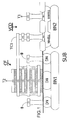
- the figure 1 represents in the form of a sectional view, a part of an integrated circuit comprising a succession of 6 layers formed of weakly resistive materials, called conductive layers, referenced (1) to (6) in ascending order from a substrate SUB to above which they are arranged. These conductive layers (1) to (6) are separated in pairs by layers of insulating material, called insulating layers, represented in the form of hatched areas in this figure.
- the layers (1) and (2) may for example be made of polysilicon, and the layers (3) to (6) of metal.
- the integrated circuit includes a first capacitive element CF having between a first and a second terminal TC1 and T2 a fixed nominal capacity.
- This capacitive element CF consists of a stack of conductive plates, cut in the conductive and electrically insulated layers of said layers.
- the first capacitive element CF comprises as many conductive plates as the integrated circuit comprises conductive layers, the first and second terminals TC1 and T2 of the first capacitive element CF being connected to the conductive plates (1) and (6) forming the ends of the stack.
- the present figure only describes the contacts connecting the first, third and fifth conductive plates (1), (3) and (5), and the first terminal TC1 of the first capacitive element CF, the contacts connecting the second, fourth and sixth plates.
- conductors (2), (4) and (6) are not in the same plane of section.
- the difference existing between the actual value and the nominal value of the capacitance of the first capacitive element CF included in such an integrated circuit is equal to the sum of the deviations caused by each of the manufacturing steps necessary for producing the integrated circuit.
- the higher the number of these manufacturing steps the lower the relative influence of each step on the difference between the actual value and the nominal value of said capacity is low.
- a first box BN1 having a conductivity type N, is implanted within the substrate SUB so that the stack forming the first capacitive element CF is superimposed on said box BN1, which is connected to the surface of the SUB substrate covered by said stack via an N-diffusion region N.
- the first well BN1 is connected to a ground potential reference terminal forming the integrated circuit via two N diffusion regions DN, each connected by contact in the third conductive layer (3) which forms, in this example, a ground plane for the integrated circuit.
- parasitic capacitance would appear between the first conductive layer (1) and the substrate SUB. This parasitic capacitance would however be dissociated from the first capacitive element CF and would degrade the quality factor thereof.
- the implantation of the box BN1 and its connection to the surface of the SUB substrate via the diffusion region N thus has a double advantage: it introduces new manufacturing steps in the process of producing the integrated circuit, thus making it possible to further reduce the dispersion.
- the integrated circuit further includes a second capacitive element VCD, for developing between a first and a second terminal a capacitance whose value depends on a set voltage applied to the first terminal, the second terminal of the second capacitive element VCD being connected to the first terminal, here called TC1, of the first capacitive element CF.
- a second capacitive element VCD for developing between a first and a second terminal a capacitance whose value depends on a set voltage applied to the first terminal, the second terminal of the second capacitive element VCD being connected to the first terminal, here called TC1, of the first capacitive element CF.
- the second capacitive element VCD is here a varicap diode, built above a second box BN2 conductivity type N implanted within the substrate SUB, a cathode and anode form respectively the first and second terminals.
- the varicap diode VCD is here produced in MOS technology, its anode and cathode respectively being constituted by P + and N + diffusion regions implanted on the surface of a NWELL well, itself disposed above the second well BN2.
- the introduction of the second capacitive element VCD has two advantages: it makes it possible to vary the capacitance value of the assembly consisting of the first and second capacitive elements CF and VCD arranged in series, and since it requires new steps of manufacture, has the effect of reducing dispersion.
- the series association of the first capacitive element CF, whose capacitance has a fixed value, with the second capacitive element has the effect of linearizing the evolution of the value of the capacitance of the assembly thus formed as a function of the value of the adjustment voltage.
- the second capacitive element is in the form of a MOS type diode, it is possible to produce such a diode in bipolar technology, the advantages described above being retained.
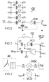
- the figure 2 is an electrical diagram equivalent to the integrated circuit part described above.
- the first capacitive element CF further comprises a capacitor C6 appearing between the first conducting layer (1) and the first well BN1, which is connected to the ground of the circuit.
- a second capacitive element VCD represented in the form of a varicap diode, is arranged in series with the first capacitive element CF, the assembly forming a capacitive branch provided with a first and a second terminal T1 and T2.
- the second capacitive element VCD is intended to develop a capacitance whose value depends on a control voltage Vtun applied to the first terminal T1.
- This adjustment voltage being in principle a DC voltage
- the cathode of the varicap diode constituting the second capacitive element VCD is, in small alternating signals, connected to the circuit ground, which is equivalent to a connection between the first and second caissons BN1 and BN2 described previously.
- This virtual connection represented in the form of a dashed line in the figure has the effect of improving the quality factor of the first capacitive branch.
- the figure 3 is a circuit diagram of an integrated circuit according to a variant of the invention which includes, in parallel with the capacitive branch described above, an inductive element L whose first terminal is connected to a power supply terminal VCC, and a second terminal of which is connected to the second terminal T2 of the first capacitive element CF.
- the assembly thus obtained forms a voltage controlled oscillator VCO whose terminal T2 is an output terminal intended to deliver an output signal Vlo whose frequency depends on the value of the control voltage Vtun.
- the second capacitive element has heretofore been described as being in the form of a MOS type varicap diode.
- FIG 4 is a block diagram describing very briefly a radio signal receiver apparatus, for example a radiotelephone, implementing an integrated circuit according to the variant of the invention described above.
- This apparatus comprises an antenna and AF filtering system, allowing the reception of a radio signal whose frequency FR, called radio frequency, is selected within a given frequency range, and its transformation into an electronic signal Vfr called radio signal.
- the apparatus also comprises a mixer MIX, intended to receive the radio signal Vfr and a signal Vlo coming from a local oscillator VCO whose frequency FLO, called oscillation frequency, is adjustable, and to deliver an output signal Vfi having an IF frequency fixed and equal to the difference between the radio frequency FR and the oscillation frequency FLO.
- the apparatus finally comprises a signal processing unit PU, intended to exploit the output signal Vfi of the mixer MIX.
- the local oscillator VCO is produced in the form of an integrated circuit as described above, intended to receive a control voltage Vtun and a selection signal Vsel1, the values of which determine the value of the oscillation frequency FLO, and therefore the value of the radio frequency FR of the selected radio signal.
Landscapes
- Semiconductor Integrated Circuits (AREA)
Claims (5)
- Integrierte Schaltung mit einer Folge von aus schwach resistiven Materialien geformten Schichten, leitende Schichten genannt, paarweise getrennt durch Schichten aus Isoliermaterial, isolierende Schichten genannt, wobei die integrierte Schaltung ein erstes kapazitives Element enthält, das zwischen einer ersten und einer zweiten Klemme eine Kapazität mit festem Nennwert hat, wobei das kapazitive Element aus einem Stapel vom leitenden Platten besteht, die innerhalb der leitenden Schichten ausgeschnitten und elektrisch von den Schichten isoliert sind, wobei die erste und die zweite Klemme des ersten kapazitiven Elements mit den leitenden Platten verbunden sind, die die Enden des Stapels bilden, wobei die integrierte Schaltung ein Substrat enthält, das als Träger für eine Wechselfolge von N isolierenden Schichten und N leitenden Schichten dient, die vom Substrat ausgehend in aufsteigender Reihenfolge nummeriert sind, dadurch gekennzeichnet, dass die i-te leitende Platte des ersten kapazitiven Elements (für i = 3 bis N) mit der (i-2)-ten leitenden Platte des kapazitiven Elements verbunden ist, wobei die erste und die zweite Klemme des ersten kapazitiven Elements mit seiner ersten bzw. N-ten leitenden Platte verbunden sind, und dass eine erste Senke mit einem gegebenen Leitfähigkeitstyp so innerhalb des Substrats installiert ist, dass der das erste kapazitive Element bildende Stapel über der Senke angeordnet ist, die mit der von dem Stapel bedeckten Fläche des Substrats über einen Bereich vom gleichen Leitfähigkeitstyp wie die Senke verbunden ist, und dass die erste Senke mit einer Bezugspotentialklemme verbunden ist, die die Masse der integrierten Schaltung bildet.
- Integrierte Schaltung nach Anspruch 1, dadurch gekennzeichnet, dass sie außerdem ein zweites kapazitives Element enthält, das dazu bestimmt ist, zwischen einer ersten und einer zweiten Klemme eine Kapazität zu entwickeln, deren Wert von einer Regelspannung abhängt, die an die erste Klemme angelegt wird, wobei die zweite Klemme des zweiten kapazitiven Elements mit einer der Klemmen des ersten kapazitiven Elements verbunden ist.
- Integrierte Schaltung nach Anspruch 2, dadurch gekennzeichnet, dass das zweite kapazitive Element eine Varicap-Diode ist, die über einer innerhalb des Substrats installierten zweiten Senke mit einem gegebenen Leitfähigkeitstyp aufgebaut ist, von der eine Kathode und eine Anode die erste bzw. die zweite Klemme bilden.
- Integrierte Schaltung nach Anspruch 3, dadurch gekennzeichnet, dass sie außerdem ein induktives Element aufweist, von dem eine erste Klemme mit einer Speiseklemme verbunden ist, und von dem eine zweite Klemme mit der zweiten Klemme des ersten kapazitiven Elements verbunden ist, wodurch eine Ausgangsklemme eines Oszillators gebildet wird, der dazu bestimmt ist, ein Ausgangssignal zu liefern, dessen Frequenz vom Wert der Regelspannung abhängt.
- Empfängergerät für Funksignale, das aufweist:- ein Antennen- und Filtersystem, das den Empfang eines funkelektrischen Signals, dessen Frequenz, Funkfrequenz genannt, aus einem gegebenen Frequenzbereich ausgewählt wird, und seine Umwandlung in ein Funksignal genanntes elektronisches Signal ermöglicht,- eine Mischstufe, die dazu bestimmt ist, das Funksignal und ein von einem lokalen Oszillator stammendes Signal zu empfangen, dessen Frequenz, Schwingungsfrequenz genannt, einstellbar ist, und ein Ausgangssignal zu liefern, das eine Frequenz hat, die festgelegt und gleich der Differenz zwischen der Funkfrequenz und der Schwingungsfrequenz ist, und- eine Verarbeitungseinheit des Signals, die dazu bestimmt ist, das Ausgangssignal der Mischstufe zu nutzen, dadurch gekennzeichnet, dass der lokale Oszillator in Form einer integrierten Schaltung nach Anspruch 4 hergestellt ist.
Applications Claiming Priority (2)
| Application Number | Priority Date | Filing Date | Title |
|---|---|---|---|
| FR9816565 | 1998-12-29 | ||
| FR9816565 | 1998-12-29 |
Publications (2)
| Publication Number | Publication Date |
|---|---|
| EP1017101A1 EP1017101A1 (de) | 2000-07-05 |
| EP1017101B1 true EP1017101B1 (de) | 2009-07-29 |
Family
ID=9534609
Family Applications (1)
| Application Number | Title | Priority Date | Filing Date |
|---|---|---|---|
| EP99204399A Expired - Lifetime EP1017101B1 (de) | 1998-12-29 | 1999-12-20 | Integrierter Schaltkreis mit einem Kapazitätsnetzwerk mit niedriger Dispersion |
Country Status (7)
| Country | Link |
|---|---|
| US (1) | US6278871B1 (de) |
| EP (1) | EP1017101B1 (de) |
| JP (1) | JP4601751B2 (de) |
| KR (1) | KR100707877B1 (de) |
| CN (1) | CN1153293C (de) |
| DE (1) | DE69941178D1 (de) |
| TW (1) | TW460929B (de) |
Families Citing this family (6)
| Publication number | Priority date | Publication date | Assignee | Title |
|---|---|---|---|---|
| EP1732091B1 (de) * | 1997-11-18 | 2009-10-07 | Panasonic Corporation | Mehrschichtprodukt, Kondensator und Verfahren zur Herstellung des Mehrschichtprodukts |
| JP4034099B2 (ja) * | 2002-03-28 | 2008-01-16 | 株式会社ルネサステクノロジ | 高周波用モノリシック集積回路装置およびその製造方法 |
| KR100450824B1 (ko) * | 2002-11-06 | 2004-10-01 | 삼성전자주식회사 | 고주파용 가변 캐패시터 구조 및 그 제조방법 |
| US7518850B2 (en) | 2006-05-18 | 2009-04-14 | International Business Machines Corporation | High yield, high density on-chip capacitor design |
| CN111192873B (zh) * | 2020-01-09 | 2020-09-04 | 华南理工大学 | 一种提高mim电容高频可靠性的版图结构及其实现方法 |
| CN112436848B (zh) * | 2020-12-04 | 2022-08-05 | 深圳市锐尔觅移动通信有限公司 | 调谐电路、射频电路及电子设备 |
Citations (1)
| Publication number | Priority date | Publication date | Assignee | Title |
|---|---|---|---|---|
| US4685197A (en) * | 1986-01-07 | 1987-08-11 | Texas Instruments Incorporated | Fabricating a stacked capacitor |
Family Cites Families (16)
| Publication number | Priority date | Publication date | Assignee | Title |
|---|---|---|---|---|
| JPS5516461B2 (de) * | 1974-03-25 | 1980-05-02 | ||
| JPH01120858A (ja) * | 1987-11-04 | 1989-05-12 | Mitsubishi Electric Corp | 集積回路装置 |
| JPH0389545A (ja) * | 1989-08-31 | 1991-04-15 | Sharp Corp | 集積回路のためのキャパシタ |
| JPH03257855A (ja) * | 1990-03-07 | 1991-11-18 | Matsushita Electron Corp | 半導体装置 |
| US5189594A (en) * | 1991-09-20 | 1993-02-23 | Rohm Co., Ltd. | Capacitor in a semiconductor integrated circuit and non-volatile memory using same |
| US5256588A (en) * | 1992-03-23 | 1993-10-26 | Motorola, Inc. | Method for forming a transistor and a capacitor for use in a vertically stacked dynamic random access memory cell |
| US5275974A (en) * | 1992-07-30 | 1994-01-04 | Northern Telecom Limited | Method of forming electrodes for trench capacitors |
| GB9416900D0 (en) * | 1994-08-20 | 1994-10-12 | Philips Electronics Uk Ltd | A variable capacitance semiconductor diode |
| US5448772A (en) * | 1994-08-29 | 1995-09-05 | Motorola, Inc. | Stacked double balanced mixer circuit |
| US5583359A (en) * | 1995-03-03 | 1996-12-10 | Northern Telecom Limited | Capacitor structure for an integrated circuit |
| JP2693928B2 (ja) * | 1995-05-24 | 1997-12-24 | 日本電気アイシーマイコンシステム株式会社 | 半導体集積回路 |
| DE69534517D1 (de) | 1995-10-31 | 2006-02-23 | St Microelectronics Srl | Herstellungsverfahren für Kondensator mit hoher Kapazität |
| US6057224A (en) * | 1996-03-29 | 2000-05-02 | Vlsi Technology, Inc. | Methods for making semiconductor devices having air dielectric interconnect structures |
| US5807775A (en) * | 1996-06-24 | 1998-09-15 | Vanguard International Semiconductor Corporation | Method for forming a double walled cylindrical capacitor for a DRAM |
| EP0836271B1 (de) * | 1996-10-10 | 2003-01-29 | Philips Electronics N.V. | Integrierter Oszillator und einen solchen Oszillator verwendendes Funktelefon |
| SE520173C2 (sv) * | 1997-04-29 | 2003-06-03 | Ericsson Telefon Ab L M | Förfarande för tillverkning av en kondensator i en integrerad krets |
-
1999
- 1999-12-20 EP EP99204399A patent/EP1017101B1/de not_active Expired - Lifetime
- 1999-12-20 US US09/467,593 patent/US6278871B1/en not_active Expired - Lifetime
- 1999-12-20 DE DE69941178T patent/DE69941178D1/de not_active Expired - Lifetime
- 1999-12-24 CN CNB991229479A patent/CN1153293C/zh not_active Expired - Fee Related
- 1999-12-27 KR KR1019990062776A patent/KR100707877B1/ko not_active Expired - Fee Related
- 1999-12-27 JP JP37145999A patent/JP4601751B2/ja not_active Expired - Fee Related
-
2000
- 2000-02-21 TW TW089102951A patent/TW460929B/zh not_active IP Right Cessation
Patent Citations (1)
| Publication number | Priority date | Publication date | Assignee | Title |
|---|---|---|---|---|
| US4685197A (en) * | 1986-01-07 | 1987-08-11 | Texas Instruments Incorporated | Fabricating a stacked capacitor |
Also Published As
| Publication number | Publication date |
|---|---|
| DE69941178D1 (de) | 2009-09-10 |
| US6278871B1 (en) | 2001-08-21 |
| JP2000216326A (ja) | 2000-08-04 |
| JP4601751B2 (ja) | 2010-12-22 |
| CN1259770A (zh) | 2000-07-12 |
| CN1153293C (zh) | 2004-06-09 |
| KR20000052585A (ko) | 2000-08-25 |
| TW460929B (en) | 2001-10-21 |
| KR100707877B1 (ko) | 2007-04-16 |
| EP1017101A1 (de) | 2000-07-05 |
Similar Documents
| Publication | Publication Date | Title |
|---|---|---|
| US5939766A (en) | High quality capacitor for sub-micrometer integrated circuits | |
| EP1636130B1 (de) | Integrierte schaltung auf hochleistungschip | |
| EP2405574B1 (de) | Vorrichtung zur Adaptation der Impedanz einer Komponente, die einen adaptierbaren Impedanzfilter auf der Basis eines Materials vom Typ Perowskit umfasst | |
| FR2593640A1 (fr) | Dispositif semi-conducteur monolithique integre comportant des transistors a jonction bipolaire, des transistors cmos et dmos, des diodes a faible fuite et procede pour sa fabrication | |
| FR2782415A1 (fr) | Dipositif de memoire a semiconducteur haute densite et son procede de fabrication | |
| EP1095407A1 (de) | Integrierter soi-schaltkreis mit entkopplungskondensator und dessen herstellungsverfahren | |
| EP0461967A2 (de) | Halbleiteranordnung mit Schottky-Übergang für Mikrowellenverstärkung und schnelle logische Schaltungen und Verfahren zu deren Herstellung | |
| EP0296997A1 (de) | MOS-Leistungstransistoranordnung | |
| FR2553583A1 (fr) | Limiteur de puissance elevee a diodes pin pour ondes millimetriques et procede de realisation des diodes | |
| EP0836271B1 (de) | Integrierter Oszillator und einen solchen Oszillator verwendendes Funktelefon | |
| EP0006474A1 (de) | Verfahren zur Korrektur des Spannungskoeffizienten von ionenimplantierten oder diffundierten Halbleiterwiderständen | |
| FR2890257A1 (fr) | Element de circuit a capacite variable | |
| EP1017102A1 (de) | Integrierter Schaltkreis mit induktiven Elementen | |
| FR2957717A1 (fr) | Procede de formation d'une structure de type metal-isolant-metal tridimensionnelle | |
| FR2515875A1 (fr) | Circuit de chaine de transistors a effet de champ | |
| EP1168442B1 (de) | Integrierte Schaltung mit Induktanz von hohem Gütefaktor und grosser Kompaktheit | |
| EP1017101A1 (de) | Integrierter Schaltkreis mit einem Kapazitätsnetzwerk mit niedriger Dispersion | |
| US5010025A (en) | Method of making trench JFET integrated circuit elements | |
| EP0169122B1 (de) | Mittels Gleichspannung steuerbares Element mit variabler Kapazität | |
| FR2775832A1 (fr) | Systeme semiconducteur de test realise dans un chemin de decoupe d'une plaquette semiconductrice | |
| FR2815774A1 (fr) | Resonateur electrique | |
| EP0928060A1 (de) | Gleichspannungswandler mit verbessertem Wirkungsgrad | |
| FR3074962A1 (fr) | Dispositif electronique capteur d'images | |
| EP1213762A1 (de) | Isolationsvorrichtung für elektrisches Bauelement | |
| FR2973970A1 (fr) | Dispositif utilisant un filtre a base de resonateurs |
Legal Events
| Date | Code | Title | Description |
|---|---|---|---|
| PUAI | Public reference made under article 153(3) epc to a published international application that has entered the european phase |
Free format text: ORIGINAL CODE: 0009012 |
|
| AK | Designated contracting states |
Kind code of ref document: A1 Designated state(s): DE FR GB |
|
| AX | Request for extension of the european patent |
Free format text: AL;LT;LV;MK;RO;SI |
|
| 17P | Request for examination filed |
Effective date: 20010105 |
|
| AKX | Designation fees paid |
Free format text: DE FR GB |
|
| 17Q | First examination report despatched |
Effective date: 20070625 |
|
| RAP1 | Party data changed (applicant data changed or rights of an application transferred) |
Owner name: NXP B.V. |
|
| GRAP | Despatch of communication of intention to grant a patent |
Free format text: ORIGINAL CODE: EPIDOSNIGR1 |
|
| GRAS | Grant fee paid |
Free format text: ORIGINAL CODE: EPIDOSNIGR3 |
|
| GRAA | (expected) grant |
Free format text: ORIGINAL CODE: 0009210 |
|
| GRAL | Information related to payment of fee for publishing/printing deleted |
Free format text: ORIGINAL CODE: EPIDOSDIGR3 |
|
| GRAS | Grant fee paid |
Free format text: ORIGINAL CODE: EPIDOSNIGR3 |
|
| AK | Designated contracting states |
Kind code of ref document: B1 Designated state(s): DE FR GB |
|
| REG | Reference to a national code |
Ref country code: GB Ref legal event code: FG4D Free format text: NOT ENGLISH |
|
| REF | Corresponds to: |
Ref document number: 69941178 Country of ref document: DE Date of ref document: 20090910 Kind code of ref document: P |
|
| PLBE | No opposition filed within time limit |
Free format text: ORIGINAL CODE: 0009261 |
|
| STAA | Information on the status of an ep patent application or granted ep patent |
Free format text: STATUS: NO OPPOSITION FILED WITHIN TIME LIMIT |
|
| 26N | No opposition filed |
Effective date: 20100503 |
|
| REG | Reference to a national code |
Ref country code: FR Ref legal event code: PLFP Year of fee payment: 17 |
|
| REG | Reference to a national code |
Ref country code: FR Ref legal event code: PLFP Year of fee payment: 18 |
|
| REG | Reference to a national code |
Ref country code: DE Ref legal event code: R081 Ref document number: 69941178 Country of ref document: DE Owner name: OCT CIRCUIT TECHNOLOGIES INTERNATIONAL LTD., IE Free format text: FORMER OWNER: NXP B.V., EINDHOVEN, NL |
|
| REG | Reference to a national code |
Ref country code: FR Ref legal event code: PLFP Year of fee payment: 19 |
|
| PGFP | Annual fee paid to national office [announced via postgrant information from national office to epo] |
Ref country code: FR Payment date: 20171121 Year of fee payment: 19 Ref country code: DE Payment date: 20171120 Year of fee payment: 19 |
|
| PGFP | Annual fee paid to national office [announced via postgrant information from national office to epo] |
Ref country code: GB Payment date: 20171121 Year of fee payment: 19 |
|
| REG | Reference to a national code |
Ref country code: DE Ref legal event code: R119 Ref document number: 69941178 Country of ref document: DE |
|
| GBPC | Gb: european patent ceased through non-payment of renewal fee |
Effective date: 20181220 |
|
| PG25 | Lapsed in a contracting state [announced via postgrant information from national office to epo] |
Ref country code: FR Free format text: LAPSE BECAUSE OF NON-PAYMENT OF DUE FEES Effective date: 20181231 Ref country code: DE Free format text: LAPSE BECAUSE OF NON-PAYMENT OF DUE FEES Effective date: 20190702 |
|
| PG25 | Lapsed in a contracting state [announced via postgrant information from national office to epo] |
Ref country code: GB Free format text: LAPSE BECAUSE OF NON-PAYMENT OF DUE FEES Effective date: 20181220 |