EP1732091B1 - Mehrschichtprodukt, Kondensator und Verfahren zur Herstellung des Mehrschichtprodukts - Google Patents
Mehrschichtprodukt, Kondensator und Verfahren zur Herstellung des Mehrschichtprodukts Download PDFInfo
- Publication number
- EP1732091B1 EP1732091B1 EP06017841A EP06017841A EP1732091B1 EP 1732091 B1 EP1732091 B1 EP 1732091B1 EP 06017841 A EP06017841 A EP 06017841A EP 06017841 A EP06017841 A EP 06017841A EP 1732091 B1 EP1732091 B1 EP 1732091B1
- Authority
- EP
- European Patent Office
- Prior art keywords
- layered product
- layer
- electrically insulating
- deposition
- thin film
- Prior art date
- Legal status (The legal status is an assumption and is not a legal conclusion. Google has not performed a legal analysis and makes no representation as to the accuracy of the status listed.)
- Expired - Lifetime
Links
Images







Classifications
-
- H—ELECTRICITY
- H01—ELECTRIC ELEMENTS
- H01G—CAPACITORS; CAPACITORS, RECTIFIERS, DETECTORS, SWITCHING DEVICES, LIGHT-SENSITIVE OR TEMPERATURE-SENSITIVE DEVICES OF THE ELECTROLYTIC TYPE
- H01G4/00—Fixed capacitors; Processes of their manufacture
- H01G4/30—Stacked capacitors
-
- H—ELECTRICITY
- H01—ELECTRIC ELEMENTS
- H01G—CAPACITORS; CAPACITORS, RECTIFIERS, DETECTORS, SWITCHING DEVICES, LIGHT-SENSITIVE OR TEMPERATURE-SENSITIVE DEVICES OF THE ELECTROLYTIC TYPE
- H01G4/00—Fixed capacitors; Processes of their manufacture
- H01G4/002—Details
- H01G4/005—Electrodes
-
- C—CHEMISTRY; METALLURGY
- C23—COATING METALLIC MATERIAL; COATING MATERIAL WITH METALLIC MATERIAL; CHEMICAL SURFACE TREATMENT; DIFFUSION TREATMENT OF METALLIC MATERIAL; COATING BY VACUUM EVAPORATION, BY SPUTTERING, BY ION IMPLANTATION OR BY CHEMICAL VAPOUR DEPOSITION, IN GENERAL; INHIBITING CORROSION OF METALLIC MATERIAL OR INCRUSTATION IN GENERAL
- C23C—COATING METALLIC MATERIAL; COATING MATERIAL WITH METALLIC MATERIAL; SURFACE TREATMENT OF METALLIC MATERIAL BY DIFFUSION INTO THE SURFACE, BY CHEMICAL CONVERSION OR SUBSTITUTION; COATING BY VACUUM EVAPORATION, BY SPUTTERING, BY ION IMPLANTATION OR BY CHEMICAL VAPOUR DEPOSITION, IN GENERAL
- C23C14/00—Coating by vacuum evaporation, by sputtering or by ion implantation of the coating forming material
- C23C14/04—Coating on selected surface areas, e.g. using masks
- C23C14/042—Coating on selected surface areas, e.g. using masks using masks
-
- H—ELECTRICITY
- H01—ELECTRIC ELEMENTS
- H01G—CAPACITORS; CAPACITORS, RECTIFIERS, DETECTORS, SWITCHING DEVICES, LIGHT-SENSITIVE OR TEMPERATURE-SENSITIVE DEVICES OF THE ELECTROLYTIC TYPE
- H01G13/00—Apparatus specially adapted for manufacturing capacitors; Processes specially adapted for manufacturing capacitors not provided for in groups H01G4/00 - H01G11/00
-
- H—ELECTRICITY
- H01—ELECTRIC ELEMENTS
- H01G—CAPACITORS; CAPACITORS, RECTIFIERS, DETECTORS, SWITCHING DEVICES, LIGHT-SENSITIVE OR TEMPERATURE-SENSITIVE DEVICES OF THE ELECTROLYTIC TYPE
- H01G4/00—Fixed capacitors; Processes of their manufacture
- H01G4/002—Details
- H01G4/018—Dielectrics
- H01G4/06—Solid dielectrics
- H01G4/14—Organic dielectrics
- H01G4/145—Organic dielectrics vapour deposited
-
- H—ELECTRICITY
- H01—ELECTRIC ELEMENTS
- H01G—CAPACITORS; CAPACITORS, RECTIFIERS, DETECTORS, SWITCHING DEVICES, LIGHT-SENSITIVE OR TEMPERATURE-SENSITIVE DEVICES OF THE ELECTROLYTIC TYPE
- H01G4/00—Fixed capacitors; Processes of their manufacture
- H01G4/30—Stacked capacitors
- H01G4/306—Stacked capacitors made by thin film techniques
-
- Y—GENERAL TAGGING OF NEW TECHNOLOGICAL DEVELOPMENTS; GENERAL TAGGING OF CROSS-SECTIONAL TECHNOLOGIES SPANNING OVER SEVERAL SECTIONS OF THE IPC; TECHNICAL SUBJECTS COVERED BY FORMER USPC CROSS-REFERENCE ART COLLECTIONS [XRACs] AND DIGESTS
- Y10—TECHNICAL SUBJECTS COVERED BY FORMER USPC
- Y10T—TECHNICAL SUBJECTS COVERED BY FORMER US CLASSIFICATION
- Y10T428/00—Stock material or miscellaneous articles
- Y10T428/24—Structurally defined web or sheet [e.g., overall dimension, etc.]
- Y10T428/24355—Continuous and nonuniform or irregular surface on layer or component [e.g., roofing, etc.]
- Y10T428/24372—Particulate matter
- Y10T428/2438—Coated
-
- Y—GENERAL TAGGING OF NEW TECHNOLOGICAL DEVELOPMENTS; GENERAL TAGGING OF CROSS-SECTIONAL TECHNOLOGIES SPANNING OVER SEVERAL SECTIONS OF THE IPC; TECHNICAL SUBJECTS COVERED BY FORMER USPC CROSS-REFERENCE ART COLLECTIONS [XRACs] AND DIGESTS
- Y10—TECHNICAL SUBJECTS COVERED BY FORMER USPC
- Y10T—TECHNICAL SUBJECTS COVERED BY FORMER US CLASSIFICATION
- Y10T428/00—Stock material or miscellaneous articles
- Y10T428/24—Structurally defined web or sheet [e.g., overall dimension, etc.]
- Y10T428/24355—Continuous and nonuniform or irregular surface on layer or component [e.g., roofing, etc.]
- Y10T428/24372—Particulate matter
- Y10T428/24405—Polymer or resin [e.g., natural or synthetic rubber, etc.]
-
- Y—GENERAL TAGGING OF NEW TECHNOLOGICAL DEVELOPMENTS; GENERAL TAGGING OF CROSS-SECTIONAL TECHNOLOGIES SPANNING OVER SEVERAL SECTIONS OF THE IPC; TECHNICAL SUBJECTS COVERED BY FORMER USPC CROSS-REFERENCE ART COLLECTIONS [XRACs] AND DIGESTS
- Y10—TECHNICAL SUBJECTS COVERED BY FORMER USPC
- Y10T—TECHNICAL SUBJECTS COVERED BY FORMER US CLASSIFICATION
- Y10T428/00—Stock material or miscellaneous articles
- Y10T428/24—Structurally defined web or sheet [e.g., overall dimension, etc.]
- Y10T428/24355—Continuous and nonuniform or irregular surface on layer or component [e.g., roofing, etc.]
- Y10T428/24372—Particulate matter
- Y10T428/24413—Metal or metal compound
Definitions
- the present invention relates to a method for producing a layered product comprising resin layers and metal thin film layers.
- the present first invention relates to a method for producing a layered product that is suitable for producing a layered product by depositing a plurality of deposition units, each of which includes a resin layer and a metal thin film layer deposited in an arbitrary shape on the resin layer.
- the present invention relates to a layered product including dielectric layers and metal thin film layers, in particular, a layered product suitably used for an electronic component such as a capacitor.
- a layered product comprising resin layers and metal thin film layers is used in a wide range of applications, for example, as a magnetic recording medium such as a magnetic tape, a wrapping material or an electronic component.
- the resin layers used in such a layered product are produced by melting and stretching a resin material into a self-supported film or by applying a solution of a resin material diluted with a solvent to a supporting base and drying the resin for curing.
- the smallest thickness of the resin layer obtained by these methods is only about 1 ⁇ m, and neither of the above methods can produce thinner resin layers stably.
- the former method tends to require large scale equipment. In the latter method, some solvents are not preferable to be used for environmental reasons, and defects tend to be generated in the coating film after drying.
- a method of vacuum evaporation on a surface of a supporting base that is moving at high speed is advantageous for mass production and is put in industrially practical use.
- metal thin film layers namely forming metal thin film layers only on a specific region
- a metal thin film layer can be divided into a plurality of sections by forming an insulating region where no metal thin film layer is formed, so that metal thin film layers having different electric potentials can be formed in a layered product.
- Oil margin is a known method for patterning the metal thin film layer. This method utilizes the following principle. When a patterning material such as oil is previously formed in a small thickness on a supporting base, and then a metal thin film is formed by metal evaporation or the like, a metal thin film layer is not formed on the patterning material.
- a layered product including resin layers and metal thin film layers are directed to further degrees of compactness, high performance and low cost. For example, various required characteristics are satisfied or a specific function is provided by depositing a plurality of deposition units comprising resin layers and patterned metal thin film layers. In this manner, efforts have been made to achieve both compactness and high performance. Moreover, efforts have been made also to achieve a low cost by depositing layers for a layered product comprising resin layers and metal thin film layers continuously on a rotating supporting base.
- the current need for compactness and high performance of electronic components is increasingly strengthened, and this is the case also for capacitors.
- the capacitance of the capacitor is in proportion to the area of the dielectric and in inverse proportion to the square of the thickness of the dielectric layer when the dielectric constant of the dielectric is the same. Therefore, in order to achieve a compact capacitor and maintain or increase the capacitance thereof, it is effective to make the dielectric layer thin and increase an effective area of a region where capacitance is generated.
- a layered product comprising dielectric layers and metal thin film layers used for electronic components such as capacitors
- This layered product is formed by layering or winding a metallized film obtained by depositing a metal thin film such as aluminum on a resin film such as polyester (e.g., PEN, PET), polyolefin (e.g., PP) or PPS by vacuum evaporation, sputtering or the like.
- a resin film such as polyester (e.g., PEN, PET), polyolefin (e.g., PP) or PPS by vacuum evaporation, sputtering or the like.
- the capacitor disclosed in Japanese Patent (Tokko-Sho) No. 63-31929 has a structure where a metal thin film layer (electrode layer) is inclined to the deposition direction so as to be in contact with the side of the capacitor, thereby forming electrodes. Therefore, the metal thin film layer is likely to be ruptured in the inclined portion of the metal thin film layer. In addition, the appearance thereof is significantly different from that of a conventional chip film capacitor, so that special consideration for mounting is required.
- U.S.P. No. 5,125,138 discloses a layered product where the metal thin film layer (electrode layer) is exposed at the side of the layered product without being inclined.
- the deposition thickness is significantly different between a portion where a small number of metal thin film layers are deposited and the other portions in the overall layered product. Therefore, a recess is generated on the upper surface in the deposition direction in the portion where a small number of metal thin film layers are deposited. This recess deteriorates the handling properties when mounting the layered product onto a printed circuit board with a solder and adversely affects the wettability of the solder.
- the deposition thickness is small, thus leading to a drop of the withstand voltage, pinholes of the dielectric layer, poor conductivity of the metal thin film layer or the like, when the layered product is used as a capacitor. Furthermore, such a recess makes it difficult to produce the layered product itself.
- the recess is generated more significantly with decreasing thickness of the dielectric layer (e.g., 1 ⁇ m or less) and with increasing-the number of depositions (e.g., 100 or more, particularly 1000 or more): Therefore, in such a layered product, it was still difficult to achieve both compactness and high capacitance of the capacitor.
- the present invention has the following embodiments.
- a first layered product of the present invention includes at least 100 deposition units, each of which includes a dielectric layer having a thickness not more than 1 ⁇ m, and a first metal thin film layer and a second metal thin film layer deposited on one surface of the dielectric layer, the first metal thin film layer and the second metal thin film layer being separated by a belt-shaped electrically insulating portion.
- the deposition position of the electrically insulating portion of the deposition unit is different from that of the deposition unit adjacent thereto, and the electrically insulating portions of every other deposition unit are not deposited in the same position in the overall layered product.
- a second layered product of the present invention includes 100 or more deposition units, each of which includes a dielectric layer having a thickness not more than 1 ⁇ m and a metal thin film layer deposited on one surface of the dielectric layer except a portion where a belt-shape electrically insulating portion is present on an end of the surface of the dielectric layer.
- the electrically insulating portions of adjacent deposition units are positioned on opposite sides, and the widths of the electrically insulating portions of every other deposition unit are not the same in the overall layered product.
- a capacitor of the present invention is formed with the first or second layered product.
- a method for producing the layered product of the present invention includes repeating a process unit a predetermined number of times, the process unit including applying a resin material so as to deposit a dielectric layer; applying a patterning material on the dielectric layer; and depositing a metal thin film layer, thereby producing a layered product comprising dielectric layers and metal thin film layers.
- the position of the 2n th (n is a natural number) application of the patterning material is different from that of the 2n-1 th application of the patterning material, and all the positions of the 2n th application, of the patterning material are not the same, and all the positions of the 2n-1 th application of the patterning material are not the same.
- the present invention has the following advantages.
- the metal thin film layer is hardly ruptured, and when it is used as a capacitor, a special consideration for mounting is not required, because it has an appearance and configuration similar to those of a conventional film capacitor, and compactness and high capacitance can be achieved.
- the method for producing the layered product of the present invention allows the above-described layered product to be produced in a simple method, efficiently and inexpensively.
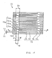
- FIG. 1 is a cross-sectional view of an example of the layered product of the present invention in the thickness direction (deposition direction).
- a layered product 11 of the present invention includes a plurality of deposition units 15, each of which includes a dielectric layer 12, a first metal thin film layer 13 and a second metal thin film layer 14 deposited on the dielectric layer 12.
- the first metal thin film layer 13 and the second metal thin film layer 14 are separated by a belt-shaped electrically insulating portion 16.
- electrically insulating portions of adjacent deposition units are required to be deposited in different positions. More specifically, as shown in FIG. 1 , in the case where the deposition unit 15 is deposited adjacent to a deposition unit 15a, the electrically insulating portion 16 of the deposition unit 15 is required to be deposited in a different position from that of the electrically insulating portion 16a of the deposition unit 15a. Thus, the deposition units having the electrically insulating portions deposited in different positions are deposited sequentially. In this case, a capacitor can be formed by forming external electrodes on the side portions of the layered product (see FIG. 11 ).
- an external electrode for connecting the first metal thin film layer 13 of the deposition unit 15 and the first metal thin film layer 13a of the deposition unit 15a adjacent thereto in substantially the same electric potential is provided
- an external electrode for connecting the second metal thin film layer 14 of the deposition unit 15 and the second metal thin film, layer 14a of the deposition unit 15a in substantially the same electric potential is provided, and an electrical potential difference is provided between the external electrodes.
- the electrically insulating portions 16 and 16a of the deposition unit 15 and the depositions unit 15a adjacent thereto are provided in different positions, a capacitor having electrodes and a dielectric (a portion where capacitance is generated) as follows is formed:
- the first metal thin film layer 13 of the deposition unit 15 and the second metal thin film layer 14a of the deposition unit 15a serve as the electrodes.
- a portion of the dielectric layer 12a that is sandwiched by the first metal thin film layer 13 and the second metal thin film layer 14a serves as the dielectric. Therefore, the phrase "the electrically insulating portions of the adjacent deposition units are deposited in different positions" means that the deposition positions are different to the extent that the capacitance generation portion of a capacitor can be formed, as described above. In such a situation, it is preferable to provide the electrically insulating portions so that the area of the capacitance generation portion becomes as large as possible.
- the second metal thin film layer 14 of the deposition unit 15 and the first metal thin film layer 13a of the deposition unit 15a do not function as the electrodes of the capacitor.
- the second metal thin film layer 14 of the deposition unit 15 and the first metal thin film layer 13a of the deposition unit -16a are significant in that they improve the adhesion strength of the external electrodes. In other words, the adhesion strength with the external electrodes depend significantly on the connection strength with the metal thin film layers, and the connection strength with the dielectric layers does not significantly contribute to it.
- the presence of these layers can improve the adhesion strength of the external electrodes when the capacitor is formed.
- the presence of such metal thin film layers is very significant especially in the case of a compact layered product as the present invention.
- the external electrodes are formed by metal spraying or the like, and sprayed-metal particles have a relatively large size. When the dielectric layer is extremely small as in the present invention, the sprayed metal particles hardly penetrate between the metal thin film layers. Moreover, since the layered product is small, an exposed metal thin film layer portion is small. Therefore, it is significantly important to make a contact area with the external electrodes as large as possible in order to ensure the adhesion strength of the external electrodes.
- the electrically insulating portion has a belt-shape having a constant width W for ease of the production.
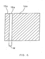
- FIG. 2 shows a cross-sectional view taken in the arrow direction of line III-III in FIG. 1 .
- the width W of the electrically insulating portion is not limited to a particular value, but preferably is about 0.03 - 0.5mm, more preferably about 0.05 - 0.4mm, and most preferably about 0.1-0.3mm to ensure the capacitance generation portion (high capacitance) of the capacitor, to ensure the electrical insulation, to facilitate the production or the like.
- the electrically insulating portion has a belt shape, and that all the deposition positions of every other electrically insulating portion are not the same position over the layered product. More specifically, as shown in FIG. 1 , with respect to the electrically insulating portion 16a of the deposition unit 15a, the position of an electrically insulating portion 16b of a deposition unit, which is one unit apart from the deposition unit 15a, is not the same position as that of the electrically insulating portion 16a, but is displaced by a distance din the width direction of the electrically insulating portion. Alternatively, the electrically insulating portion of the deposition unit one unit apart is in the same position, and the electrically insulating portion of the deposition unit three units apart can be displaced in the width direction of the electrically insulating portion.
- the thickness of the deposition of this portion is smaller relative to the overall layered product so that significant recesses 32a and 32b are generated on the upper surface of the layered product. These recesses may deteriorate the handling properties when mounting the layered product onto a printed circuit board with a solder.
- the generation of the recess causes inclination of the dielectric layer and the metal thin film layer deposited on the recess at both sides of the electrically insulating portion, so that the thickness of the deposition in portions 33a and 33b of the dielectric layer and portions 34a and 34b of the metal thin film layer becomes small locally.
- the thickness of the deposition of the dielectric layer becomes small locally, the following problem arises.
- the presence of that portion reduces the withstand voltage of the capacitor and causes a short-circuit due to pin-holes in the dielectric layer. Moreover, when the thickness of the deposition of the metal thin film layer becomes small locally, the withstand current property is likely to deteriorate in that portion.
- the lower limit of the displacement amount d of the electrically insulating.portion in FIG. 1 is preferably W/20 or more, and more preferably W/10 or more, where W is the width of the belt-shaped electrically insulating portion.
- the upper limit of the displacement amount d is preferably 4W or less, and more preferably 2W or less.
- the lower limit is preferably 6W/5 or more, and more preferably 3W/2 or more, and the upper limit is preferably 5W or less, and more preferably 4W or less.
- the maximum displacement width D 0 is lower than this lower limit, as described with reference to FIG. 3 , recesses 32a and 32b are generated on the upper surface of the layered product, so that the application of a patterning material becomes difficult.
- the drop of withstand voltage of the capacitor and generation of pinholes in portions 33a and 33b of the dielectric layer, and the deterioration of the withstand current property in the portions 34a and 34b in the metal thin film layer are likely to occur.
- the maximum displacement width D 0 is higher than this upper limit, not only is the effect of eliminating the recess on the upper surface of the layered product insignificant, but also the size of the capacitor generation portion for the capacitor small.
- deposition positions of the electrically insulating portions of every other deposition unit can be displaced regularly or irregularly (excluding discrepancies in production).
- the first metal thin film layer of a deposition unit is not electrically connected directly to the first metal thin film of the adjacent deposition unit (e.g., 13 and 13a), and/or the second metal thin film layer of a deposition unit is not electrically connected directly to the second metal thin film of the adjacent deposition unit (e.g., 14 and 14a).
- Connecting directly (contacting) the metal thin film layers means that there is no dielectric layer between them. This causes the metal thin film layer to incline toward a connecting portion, so that the metal thin film layer becomes thin in the inclined portion, which may result in a rupture.
- FIG. 4 is a cross-sectional view of another example of the layered product of the present invention in the thickness direction (deposition direction).
- a layered product 40 of this example includes a plurality of deposition units 44, each of which includes a dielectric layer 41, a metal thin film layer 42 deposited on one surface of the dielectric layer.
- the metal thin film layer 42 is not present in a belt-shaped electrically insulating portion 43 that is present on one end of the dielectric layer.
- electrically insulating portions of adjacent deposition units are required to be deposited on opposite sides. More specifically as shown in FIG. 4 , in the case were, a deposition unit 44a is deposited adjacent to a deposition unit 44, and when an electrically insulating portion 43 of the deposition unit 44 is on the right end of the dielectric layer 41, it is required that an electrically insulating portion 43a in the deposition unit 44a is provided on the left end of a dielectric layer 41a. In this manner, the deposition units are deposited sequentially in such a manner that the electrically insulating portions are positioned on the opposite sides, Thus, when external electrodes are formed on the side portions of the layered product (see FIG. 17 ), a capacitor can be formed.
- one external electrode is connected to the metal thin film layer 42 of the deposition unit 44
- the other external electrode is connected to the metal thin film layer 42a of the adjacent deposition unit 44a
- an electrical potential difference is provided between the opposite external electrodes.
- the thus formed capacitor has the metal thin film layer 42 of the deposition unit 44 and the metal thin film layer 42a of the deposition unit 44a as the electrodes, and a portion sandwiched between the metal thin film layer 42 and the metal thin film layer 42a as the dielectric (capacitance generation portion). Therefore, it is preferable that the width of the electrically insulating portion is as small as possible so as to make the area of the capacitance generation portion as large as possible.
- the shape of the electrically insulating portion is a belt-shape having a constant width W to facilitate the production.
- FIG. 5 is a cross-sectional view taken in the arrow direction of line IV-IV in FIG. 4 .
- the width W of the electrically insulating portion is not limited to a particular value, but preferably is about 0.03 to 0.5mm, more preferably about 0.05 to 0.4mm, and most preferably about 0.1 to 0.3mm to allow high capacitance of the capacitor, to ensure the electrical insulation and to facilitate the production.
- the width of the belt-shaped electrically insulator of every other deposition unit are not the same over the layered product. More specifically, as shown in FIG. 4 , with respect to an electrically insulating portion 43 of a deposition unit 44, the width of an electrically insulating portion 43b of the deposition unit that is one unit apart from the deposition unit 44 is different from that of the electrically insulating portion 43. Alternatively, the width of the electrically insulating portion is the same as that of the electrically insulating portion of the deposition unit that is one unit apart, and the width of the electrically insulating portion of the deposition unit three units apart can be changed.
- the end portion where the electrically insulating portions are provided has a small number of metal thin film layers. Therefore, the thickness of the deposition of this portion is smaller relative to the overall layered product so that a significant recess is generated on the upper surface of the layered product.
- This recess may deteriorate the handling properties when mounting the layered product onto a printed circuit board with a solder and may adversely affect the wettability of the solder.
- the larger the depth of the recess is, the more difficult it is to apply a patterning material onto the bottom of the recess as described later in the production process of the layered product.
- the generation of the recess causes inclination of the dielectric layer and the metal thin film layer deposited on the recess at a side of the electrically insulating portion, so that the thickness of the deposition of the dielectric layer and the metal thin film layer becomes small locally.
- the thickness of the deposition of the dielectric layer becomes small locally, the following problem arises.
- the presence of that portion reduces the withstand voltage of the capacitor and causes a short-circuit due to pin-holes in the dielectric layer.
- the withstand current property is likely to deteriorate in that portion.
- (W MAX -W MIN) /WAVE is preferably W AVE/5 x length unit or more, and more preferably W AVE/3 x length unit or more, where WAVE is the average width of the electrically insulating portions of every other deposition unit in the overall layered product, W MAX is the maximum thereof and W MIN is the minimum thereof, as shown in FIG. 4 .
- the upper limit of (W MAX-W MIN) / W AVE is preferably equal to or less than W AVE/1 x length unit, and more preferably W AVE/2 x length unit or less.
- the width of the electrically insulating portion of every other 1 x length unit deposition unit can be changed regularly or irregularly (excluding discrepancies in production).
- the thickness T1 ( FIG. 1 ) or T3 ( FIG. 4 ) of the dielectric layer (thickness of the capacitance generation portion) is preferably 1 ⁇ m or less, more preferably 0.7 ⁇ m or less, and most preferably 0.4 ⁇ m or less.
- a thinner dielectric layer (capacitance generation portion) can provide a capacitor having large capacitance when the layered product is used as a capacitor.
- the thickness T2 of the first metal thin film layer and the second metal thin film layer of the layered product in FIG. 1 and the thickness T4 of the layered product in FIG. 4 are not limited to particular values, but preferably 100 to 500 ⁇ , and more, preferably 200 to 400 ⁇ .
- the film resistance is preferably 10 ⁇ /cm 2 or less, and more preferably 1 to 8 ⁇ /cm 2 , and most preferably 2 to 6 ⁇ /cm 2 .
- the thicknesses of the two metal thin film layers in FIG. 1 can be different from each other, but the same thickness is preferable because a uniform thickness of the overall layered product can be obtained.
- the number of depositions for the deposition units of the layered products in FIGs. 1 and 4 can be determined suitably, depending on the application of the layered product, but is preferably 100 or more, because the area that the capacitor occupies on the circuit board can be small.
- the dielectric layer is thin, the overall thickness is not very large even if the number of depositions is large. Compared with a conventional film capacitor, the thus obtained capacitor has higher capacitance with the same volume, or is smaller with the same capacitance.
- the ratio T1/T2 or T3/T4 of the thickness T1 ( FIG. 1 ) or T3 ( FIG. 4 ) of the dielectric layer to the thickness T2 ( FIG. 1 ) or T4 ( FIG. 4 ) of the metal thin film layer of each deposition unit is preferably 20 or less, more preferably 15 or less.
- the ratio in this range is preferable for the following reasons.
- the material of the dielectric layer is not limited to the material of the dielectric layer as long as it can be deposited to a thickness of 1 ⁇ m or less and can function as a dielectric satisfactorily, but a material comprising an acrylate resin or a vinyl resin as its main component is preferable. More specifically, a polymer of a polyfunctional (meth) acrylate monomer or polyfunctional vinyl etcher monomer is preferable. Of these, for example, a polymer of a dicyclopentadiene dimethanoldiacrylate or cyclohexane dimethanoldivinylether monomer or a polymer of a monomer with substituted hydrocarbon groups is preferable because of their electric properties.
- the material of the metal thin film layer at least one selected from the group consisting of Al, Cu, Zn, Sn, Au, Ag, and Pt is preferable.
- A1 is preferable because of its deposition property and cost-efficiency.
- the surface roughness Ra (ten point average-roughness) of the dielectric layer is preferably not more than 0.1 ⁇ m, more preferably not more than 0.02 ⁇ m.
- the surface roughness Ra (ten point average roughness) of the metal thin film layer is preferably not more than 0.1 ⁇ m, more preferably not more than 0.02 ⁇ m. If the surface roughness is too large, electric field concentrations occur in small protrusions on the surface, and the dielectric layer may be damaged or the metal thin film layer may be burnt.
- external particles for example, inorganic particles such as silica or organic particles
- the surface roughness Ra (ten point average roughness) of the present invention is measured with a contact-type surface meter having a diamond needle of 10 ⁇ m tip diameter and a 10mg measuring load.
- the curing degree of the dielectric layer is preferably 50% or more, in particular, 50 - 75% in the state of the layered product immediately after formation of the dielectric layer, and preferably 90% or more in the state of the final form such as a capacitor or the like because of its handling properties or stability of the characteristics.
- the curing degree means the extent of polymerization and / or cross-linking when the resin is used as the dielectric layer. If the curing degree is below these ranges, the layered product easily can be deformed by external pressure, which occurs for example in the step of pressing in the production process of the layered product or mounting the layered product. This also can lead for example to ruptures or short-circuits of the metal thin film layer.
- the curing degree is above the above ranges, the following problems may arise.
- sprayed metal particles hardly penetrate between the metal thin film layers so that the adhesion strength of the external electrodes may be reduced; or the layered product may break, for example when the cylindrical continuous layered product is removed from the can roller in the production process of the layered product as described later, or when pressed into a flat layered base element.
- the reinforcement layer is intended to prevent the layered product portion from being damaged by thermal load or external pressure in the process of manufacturing the layered product, in the production process of an electronic component using the same, especially a capacitor, or in the process of mounting the same on a printed circuit board.
- the reinforcement layer includes a metal thin film layer, as described later, it is effective to provide the reinforcement layer in order to increase the adhesion strength of the external electrodes (see FIGs. 11 and 17 ). That is to say, the adhesion strength of the external electrodes mainly is affected by the strength of the connection with the metal thin film layer, whereas the strength of the connection with the dielectric layer contributes only little to the adhesion strength.
- the adhesion strength of the external electrode of the capacitor can, be significantly increased.
- the reinforcement layer can function as a capacitance generation portion of the capacitor, but the capacitor design can be simplified when it does not function as such.
- the effects as described above can be provided by forming the reinforcement layer only on at least one side of the layered product. However, it is more effective to form the reinforcement layer on both sides for protection of the layered product and improvement of the adhesion strength of the external electrode.
- the reinforcement layer can be deposited in contact with the layered product or can have another layer therebetween.
- the thickness (overall thickness on one surface) of the, reinforcement layer is preferably 20 ⁇ m or more, more preferably 50 to 500 ⁇ m, and.most preferable 100 to 300 ⁇ m to provide the above-described effects of the reinforcement layer sufficiently.
- FIG. 6 is a cross-sectional view taken in the thickness direction (deposition direction) of an example of the layered product, 11 in FIG. 1 described in Embodiment 1 comprising reinforcement layers 50a and 50b deposited on both sides thereof.
- the reinforcement layer shown in FIG. 6 includes at least one deposition unit 54 that includes a resin.layer 51, a first metal layer 52 and a second metal layer 53 deposited on one surface of the resin layer 51.
- the first metal layer 52 and the second metal layer 53 are separated by an electrically insulating band 55.
- the metal layer is separated into the first metal layer 52 and the second metal layer 53 by the electrically insulating band 55. If there is no electrically insulating bands, when external electrodes (see FIGs. 11 and 17 ) are provided, the external electrodes would be short-circuited via the metal layer.
- the position in which the electrically insulating band is provided is not limited to a particular position, but it is preferable to provide it substantially in the central portion of the reinforcement layer, as shown in FIG. 6 .
- a large recess may be generated on the upper surface of the layered product. Therefore, for example in mounting onto a printed circuit board with a solder, the handling properties are poor and the wettability of the solder may be adversely affected.
- the handling properties are poor and the wettability of the solder may be adversely affected.
- the generation of the recess causes inclination of the dielectric layer and the metal thin film layer deposited on the recess at both sides of the electrically insulating portion, so that the thickness of the deposition becomes small. Therefore, a reduction of the withstand voltage as a capacitor, pinholes of the dielectric layer and deterioration of the withstand current property of the metal thin film layer are likely to occur.
- the shape of the electrically insulating band is not limited to a particular shape, as long as it electrically insulates the first metal layer 52 and the second metal layer 53. In this embodiment, it is a belt shape having a constant width W 1 to facilitate the production.
- FIG. 7 is a cross-sectional view taken in the arrow direction of line V-V in FIG. 6 .
- the reinforcement layer comprises at least one deposition unit 54.
- the deposition positions of the electrically insulating bands are not the same position over the reinforcement layer (the overall reinforcement layer on one side in the case where the reinforcement layer is provided on both sides of the layered product 11).
- the electrically insulating band is a belt-shaped band having a constant width W 1 , as shown in FIG. 6 , it is preferable that the displacement amount d 1 of the electrically insulating bands of adjacent positions is W 1 /20 or more.
- the lower limit of the displacement amount d 1 is preferably W 1 /15 or more, and more preferably W 1 /10 or more.
- the upper limit is preferably 4W 1 or less, and more preferably 2W 1 or less.
- the electrically insulating bands of adjacent deposition units can be deposited in the same position, and the position of the electrically insulating band of every other (or every second or more) deposition unit can be displaced by the displacement amount d 1 .
- a recess may be generated in the electrically insulating portion on a surface of the layered product. Therefore, the handling properties may be poor when mounting the layered product onto a printed circuit board with a solder.
- a recess is generated, as the depth of the recess is larger, it is more difficult to apply a patterning material to the bottom of the recess as described later. Therefore, it is difficult to form a good electrically insulating band or electrically insulating portion having a constant width.
- the generation of the recess causes inclination of the dielectric layer and the metal thin film layer deposited on the recess at both sides of the electrically insulating portion, so that the thickness of the deposition becomes small. Therefore, a reduction of the withstand voltage as a capacitor, pinholes of the dielectric layer and a reduction of the withstand current property of the metal thin film layer are likely to occur.
- the lower limit is preferably 6W 1 /5 or more, and more preferably 3W 1 /2 or more, and the upper limit is preferably 5W 1 or less, and more preferably 4W 1 or less.
- the maximum displacement width D 1 is below this lower limit, a recess is generated on the surface of the layered product, resulting in the above-described problems.
- FIG. 8 is a cross-sectional view taken in the thickness direction (deposition direction) of an example of a layered product comprising reinforcement layers 60a and 60b having a deposition form different from that in FIG. 6 deposited on both sides of the layered product 11 in FIG. 1 described in Embodiment 1.
- the reinforcement layer shown in FIG. 8 includes at least one deposition unit 64 that includes a resin layer 61 and a metal layer 62 deposited on one surface of the resin layer. There is no metal layer in a belt-shaped electrically insulating portion 63 on one end of the surface of the resin layer. If there is no electrically insulating bands, when external electrodes (see FIGs. 11 and 17 ) are provided, the external electrodes would be short-circuited via the metal layer.
- the shape of the electrically insulating band is not limited to a particular shape, but in this embodiment, it is a belt shape having a constant width to facilitate the production or the like.
- FIG. 9 is a cross-sectional view taken in the arrow direction of line VI-VI in FIG. 8 .
- the reinforcement layer comprises at least one deposition unit 64.
- the widths of the electrically insulating bands are not the same over the reinforcement layer (the overall reinforcement layer on one side in the case where the reinforcement layer is provided on both sides of the layered product 11).
- the width of the electrically insulating band of an adjacent deposition unit is changed and further the width of the electrically insulating band of an adjacent deposition unit is changed. Thereafter, the width of the electrically insulating band is sequentially changed in the same manner.
- the widths of the electrically insulating bands of two (or more) consecutive deposition units can be the same, and the width of the electrically insulating band of the third (or more) deposition unit can be changed.
- the number of deposited metal thin film layers is small in the end portion where the electrically insulating bands are formed so that the deposition thickness in this portion is small relative to the overall layered product.
- a significant recess may be generated on the upper surface of the layered product. This recess may deteriorate the handling properties when mounting the layered product onto a printed circuit board with a solder and may adversely affect the wettability of the solder.
- a recess is generated, as the depth of the recess is larger, it is more difficult to apply a patterning material to the bottom of the recess as described later in the production process of the layered products.
- the generation of the recess causes inclination of the dielectric layer and the metal thin film layer deposited on the recess at a side of the electrically insulating portion of the layered product 11, so that the thickness of the deposition of the dielectric layer and the metal thin film layer becomes small locally
- the thickness of the deposition of the dielectric layer becomes small locally, the following problem arises.
- the layered product is used as a capacitor, the presence of that portion reduces the withstand voltage of the capacitor and causes a short-circuit due to pin-holes in the resin thin film layer.
- poor conductivity is likely to occur in that portion.
- (W 1 MAX-W 1 MIN)/W AVE is preferably W 1 AVE/5 x length unit or more, and more preferably W 1 AVE/3 x length unit or more, where W 1 AVE is the average width of the electrically insulating bands in the overall reinforcement layer (overall reinforcement layer on one side in the case where the reinforcement, layer is provided on both sides of the layered product 11), W i MAX is the maximum thereof, and W 1 MIN is the minimum thereof, as shown in FIG. 25.
- the upper limit of (W 1 MAX-W 1 MIN) / W 1 AVE is preferably W 1 AVE / length unit or less, and more preferably W 1 AVE/2 x length unit or less.
- the widths of the electrically insulating bands can be changed regularly or irregularly (excluding discrepancies in production).
- the thickness T5 ( FIG. 6 ) or T7 ( FIG. 8 ) of the resin layer of the reinforcement layer is preferably larger than the thickness T1 ( FIG. 1 ) or T3 ( FIG. 4 ) of the dielectric layer of the layered product in FIG. 1 or 4 .
- the thickness T6 ( FIG. 6 ) or T8 ( FIG. 8 ) of the metal layer of the reinforcement layer is preferably larger than the thickness T2 ( FIG. 1 ) or T4 ( FIG. 4 ) of the metal thin film layer of the layered product in FIG. 1 or 4 .
- the reinforcement layer has thick layers, so that when external electrodes described later are provided (see FIGs. 11 and 17 ), the adhesion strength of the external electrodes can be improved.
- the external electrodes are formed by spraying or the like, and the particles of sprayed metal are relatively rough and hardly penetrate between the metal thin film layers of the layered product 11 or 40 sufficiently.
- the thickness of the dielectric layer cannot be made large to ensure the capacitance for a capacitor. Therefore, the penetration of the sprayed metal is facilitated by making the thickness of the resin layer thick, and thus the adhesion strength of the external electrodes can be improved with ease.
- the thicker the metal layer exposed to the side is, the larger the tensile strength is. Therefore, the adhesion strength of the external electrodes can be improved by making the thickness of the metal layer thick.
- the thickness T5 or T7 of the dielectric layer is preferably 0.1 to 1 ⁇ m, and more preferably 0.1 to 0.6 ⁇ m.
- the thickness T6 or T8 of the metal layer is preferably 100 to 500 ⁇ , and more preferably 200 to 400 ⁇ .
- the film resistance is preferably 1 to 10 ⁇ /cm 2 or less, and more preferably 2 to 6 ⁇ /cm 2 .
- the thicknesses of the first metal layer and the second metal layer in FIG. 6 can be different from each other, but the same thickness is preferable because a uniform thickness of the overall layered product can be obtained.
- the materials for the resin layer and the metal layer of the reinforcement layer are not limited to particular materials.
- the materials used for the dielectric layer and the metal thin film layer are preferably for the resin layer and the metal layer, respectively, in view of production efficiency.
- materials different from those for the dielectric layer and the metal thin film layer are preferable for the purpose of adjusting the adhesion strength with external electrodes or adjusting the curing degree or the mechanical strength of the overall layered product or the like.
- the curing degree of the resin layer of the reinforcement layer is preferably 50% or more, in particular, 50-75% in the state immediately after formation of the reinforcement layer, and preferably 90% in the state of the final form such as a capacitor or the like because of its handling properties or stability of the characteristics. If the curing degree is below these ranges, the layered product easily can be deformed by external pressure, which occurs for example in the step of pressing in the production process of the layered product or mounting the layered product. On the other hand, if the curing degree is above the above ranges, the following problems may arise.
- sprayed metal particles When forming external electrodes, sprayed metal particles hardly penetrate between the metal layers so that the adhesion strength of the external electrodes may be reduced; or the layered product may break, for example when the cylindrical layered product is removed from the can roller in the production process of the layered product as described later, or when pressed into a flat layered base element.
- the reinforcement layer can be provided in the layered product 40 in FIG. 4 , instead of the layered product 11 in FIG. 1 , in the same manner as above.
- the above description can be applied by substituting the elements of the layered product 11 with the elements of the layered product 40 in FIG. 4 , where necessary.
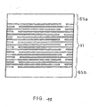
- FIG. 10 is a cross-sectional view taken in the thickness direction (deposition direction) of an example of a layered product comprising protective layers 65a and 65b deposited on both sides of the layered product 11 in FIG. 1 .
- the effects as described above can be provided by forming the protective layer only on at least one side of the layered product 11. However, it is more effective to form the protective layer on both sides for protection of the layered product 11.
- the thickness of the protective layer can be determined suitably depending on the environment to which the layered product is exposed or the like, but is preferably 2 ⁇ m or more, more preferably 3 to 100 ⁇ m, and most preferably 5 to 20 ⁇ m to provide the above-described effects sufficiently.
- the protective layer is provided directly in the layered product 11.
- the reinforcement layer described in Embodiment 4, which is interposed between the protective layer and the layered product 11.
- a layer other than the reinforcement layer can be deposited.
- the material for the protective layer there is no limitation regarding the material for the protective layer.
- the material used for the dielectric layer and/or the resin layer is preferable in view of production efficiency.
- a material different from that for the dielectric layer and/or the resin layer can be used for the purpose of providing a specific function for the protection layer.
- the protective layer can be colored to a specific color. This allows an improvement in accuracy of pattern recognition when mounting the layered product on a printed circuit board as an electronic component or facilitates the identification of each product. For example, coloring can be performed by mixing a colorant such as a pigment or coating the outer surface with a paint. Moreover, the protective layer can be made transparent, if necessary.
- the curing degree of the protective layer is preferably 50% or more, in particular, 50 - 75% in the state of the layered product immediately after formation of the protective layer, and preferably 90% in the state of the final form such as a capacitor or the like, because of its handling properties or stability of the characteristics. If the curing degree is below these ranges, the layered product easily can be reformed by external pressure, which occurs for example in the step of pressing in the production process of the layered product or mounting the layered product. On the other hand, if the curing degree is above the above ranges, the layered product may break, for example when the cylindrical continuous layered product is removed from the can roller in the production process of the layered product as described later, or when pressed into a flat layered base element.
- the protective layer can be provided in the layered product 40 in FIG. 21, instead of the layered product 11 in FIG. 1 , in the same manner as above.
- the above description can be applied by substituting the elements of the layered product 11 with the elements of the layered product 40 in FIG. 4 , where necessary.
- FIG. 11 is a schematic cross-sectional view of an example of a layered product with external electrodes 71a and 71b on sides of the layered product.
- reinforcement layers 73a and 73b are deposited on both sides of a layered product portion 72, and protective layers 74a and 74b are deposited further thereon.
- the layered product 11 described in Embodiment 3 with reference to FIG. 1 is used as the layered product portion 72.
- the reinforcement layers 50a and 50b described in Embodiment 4 with reference to FIG. 6 are used as the reinforcement layers 73a and 73b.
- the protective layers 65a and 65b described in Embodiment 5 with reference to FIG. 10 are used as the protective layers 74a and 74b.
- the external electrodes 71a and 71b are electrically connected to the first metal thin film layer and the second metal thin film layer of the layered product 72, respectively.
- the external electrodes can be formed by metal spraying with brass or the like.
- the external electrodes can be constituted of a plurality of layers by spraying different types of metals
- an underlying layer is formed by spraying a metal having good adhesion strength with the layered product, and then an upper layer is provided thereon by spraying a metal having good adhesiveness with various metals or a resin to be contracted (deposited) further on the upper layer.
- melt solder plating, melt tinning, electroless solder plating or the like can be performed.
- the following layer can be formed: a layer obtained by applying a conductive paste where copper powder or the like is dispersed in a thermosetting phenol resin and heating for curing; or a layer obtained by spraying a metal such as an alloy comprising copper / phosphorus / silver.
- a bump electrode can be provided in the external electrode to facilitate the mounting onto a circuit board further.
- the bump electrode can be formed by selecting a material suitably from known materials or shapes.
- a necessary outer package in accordance with the intended application can be provided.
- a coating about several tens of angstroms thick is provided using a surface treatment agent such as a silane coupling agent for the purpose of improving resistance of the layered product against humidity or protecting exposed metal thin film layers and / or metal layers.
- a layer obtained by applying a photocurable or thermosetting resin to a thickness of about several hundreds ⁇ m and curing the resin can be provided.
- the thus obtained layered product of the present invention can be used as a chip capacitor, a chip coil, a chip resistor, and a composite element including these, and used suitably as an electronic component such as a capacitor.
- the layered product of the present invention can be a capacitor having high capacitance, although it is small. Therefore, when it is used as a chip capacitor, the practical value is high.
- the layered product 40 in FIG. 21 can be used as the layered product 72.
- the above description can be applied by substituting the elements of the layered product 11 with the elements of the layered product 40 in FIG. 4 , where necessary.
- the reinforcement layers 50a and 50b in FIG. 6 the reinforcement layers 60a and 60b in FIG. 8 can be used as the reinforcement layers 73a and 73b.
- the above description can be applied by substituting the elements of the reinforcement layers 50a and 50b with the elements of the reinforcement layers 60a and 60b in FIG. 25, where necessary.
- FIG. 12 is a schematic view illustrating an example of a production apparatus for producing the layered product of the present invention.
- a metal evaporation source 84 is provided at a lower portion of a can roller 81, which rotates in the direction of the arrow in FIG. 12 with constant angular velocity or constant circumferential velocity.
- a resin evaporation source 82 is provided downstream in the rotation direction of the can roller 81, and an apparatus 83 for applying patterning material is provided upstream thereof.
- an apparatus 87 for removing patterning material is provided between the metal evaporation source 84 and the resin evaporation source 82, and an apparatus 88 for curing resin and an apparatus 89 for treating a resin surface are provided between the resin evaporation source 82 and the apparatus 83 for applying patterning material.
- these apparatuses can be omitted if desired, and are not indispensable to the present invention.
- the apparatuses are installed inside a vacuum container 85, in which a vacuum is maintained with a vacuum pump 86.
- the circumferential surface of the can roller 81 is smooth, preferably mirror-finished, and cooled preferably to -20°C to 40°C, more preferably - 10°C to 10°C.
- the rotation velocity can be adjusted freely, but preferable is about 15 to 70rpm.
- the metal evaporation source 84 allows metal evaporation toward the surface of the can roller 81 to form the metal thin film layer of the layered product and the metal layer of the reinforcement layer.
- the evaporation metal for example, at least one selected from the group consisting of Al, Cu, Zn, Sn, Au, Ag, and Pt can be used.
- the metal thin film can be formed by a known technique such as sputtering, ion plating or the like.
- the resin evaporation source 82 allows a reactive monomer resin to evaporate or vaporize toward the surface of the can roller 81.
- the resin is deposited so as to form the dielectric layer, the resin layer of the reinforcement layer and the protective layer.
- the deposited reactive monomer resin can be polymerized and / or cross-linked with the apparatus 88 for curing resin and cured to a predetermined curing degree.
- the apparatus for curing resin an electron beam irradiation device or a UV beam irradiation device can be used, for example.
- the surface of the formed resin thin film is treated, with the apparatus 89 for treating a resin surface.
- the surface of the resin layer can be activated with an oxygen plasma to increase the adhesiveness with the metal thin film.
- the apparatus 83 for applying patterning material deposits a patterning material on the surface of the resin thin film in a predetermined shape. No metal thin film is formed at the portions where the patterning material has been deposited.
- the patterning material for example, oil can be used.
- evaporated and vaporized patterning material can be ejected from pinholes and condensed on the surface of the resin thin film, or liquid patterning material can be ejected.
- contactless application methods other application methods such as reverse coating or die coating are possible, but for the present invention, contactless application methods are preferable because no external pressure is applied to the resin surface.
- a method of condensing the evaporated patterning material on the surface of the resin thin film is preferable because the structure is relatively simple.
- FIG. 13 is a schematic perspective view of an apparatus for applying patterning material that applies a belt-shaped oil film on a surface of a resin thin film by ejecting evaporated oil as an example of the apparatus for applying patterning material.
- the apparatus is provided in such a manner that a plane 91 of the apparatus 83 for applying patterning material is perpendicular to the normal line of the circumferential surface of the can roller 81.
- a predetermined number of pinholes 92 for ejecting vaporized oil are arranged at predetermined intervals.
- the shape of the pinholes 92 can be round, as shown in FIG. 13 , but elliptical, elongated, rectangular or other shapes are also possible.
- a plurality of elliptical, elongated, or rectangular pinholes can be arranged in the travel direction of the surface of the can roller.
- the patterning material applied with the apparatus 83 for applying patterning material can be removed by an apparatus 87 for removing patterning material, if necessary. Most of the patterning material that has been deposited with the apparatus for applying a patterning material is removed by being again evaporated when the metal thin film layer is formed. However, a portion remains even after the formation of the metal thin film layer, and can contribute to a number of problems, such as chapping the deposited surface, causing pinholes (lack of deposition) in the dielectric layer or the metal thin film layer, or instabilities in the regions where the metal thin film layer is deposited.
- the patterning material should be applied in the minimum amount necessary so that it is not present after the formation of the metal thin film layer.
- the control thereof is very difficult. Therefore, it may be preferable to remove the residual patterning material after the metal thin film layer has been deposited and before the dielectric layer is deposited.
- the patterning material is removed by heat evaporation by a heater, or decomposition by plasma irradiation, or a combination thereof.
- oxygen plasma, argon plasma, nitrogen plasma, or the like can be used for the plasma irradiation, but among these, oxygen plasma is most preferable.
- the layered product of the present invention is produced by repeating a process unit a predetermined number of times, the process unit including applying a resin material with the resin evaporation source 82, thereby forming a dielectric layer, applying a patterning material on the dielectric layer with the apparatus 83 for applying patterning material, and depositing a metal thin film layer with the metal evaporation source 84.
- the 2n th (n is a natural number) application of the patterning material is performed in a different position from that of the 2n-1 th application. Moreover, all the positions of the 2n th application of the patterning material are not the same, and all the positions of the 2n-1 th application of the patterning material are not the same.
- an electrically insulating portion is formed in a belt-shape in a non-end portion of the dielectric layer, and the deposition positions of the electrically insulating portions of adjacent deposition units are different. In addition, the deposition positions of the electrically insulating portions of every other deposition unit are not the same in the overall layered products.
- an electrically insulating portion is formed in a belt-shape in an end portion of the dielectric layer, and the electrically insulating portions of adjacent deposition units are positioned on opposite sides.
- the widths of the electrically insulating portions of every other deposition unit are not the same in the overall layered product.
- the displacement amount of the deposition positions of the electrically insulating portions of every other deposition unit is W/20 or more and not more than 4W, where W is the width of the belt-shaped electrically insulating portion.
- both the maximum of the variations of the positions of the 2n th application of the patterning material and the maximum of the variations of the positions of the 2n-1 th application of the patterning material are 6W/5 to 5W, where W is the application width of the belt-shaped patterning material.
- the maximum of the variations of the deposition positions of the electrically insulating portions of every other deposition unit are 6W/5 to 5W in the overall layered product.
- the apparatus:83 for applying patterning material as the deposition progresses not only in the case where the patterning material is directly applied by coating or the like, but also in the case where deposition is performed by a contactless method.
- the pattering material diffuses with a certain directionality especially when vaporized oil is ejected for deposition, so that a variation of the distance Dw changes the application width, whereby the electrically insulating portion having a predetermined width cannot be obtained stably.
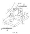
- the retraction of the apparatus for applying patterning material and the movement of the deposition position of the patterning material can be performed, for example by an apparatus as shown in FIG. 14 .
- the apparatus for applying patterning material is retracted in the following manner.
- An actuator A 102 is fixed on a movable base 101.
- the apparatus 83 for applying patterning material is attached to the mobile end of the actuator A 102.
- the actuator A 102 can move the apparatus 83 for applying patterning material in the direction of arrow 103 on the movable base 101.
- a gap measuring device 104 for measuring the distance to the surface of the can roller 81 (the circumferential surface of the layered product in the process of the formation of the layered product) is provided on the apparatus 83 for applying patterning material.
- a contactless measuring device for example a measuring device using a laser, can be used for the gap measuring device 104.
- the gap measuring device 104 keeps measuring the distance to the circumferential surface of the layered product on the surface of the can roller 81, and a signal corresponding to this measurement is sent to a gap measuring circuit 105.
- the gap measuring circuit 105 continuously checks whether the distance between the nozzle end of the apparatus 83 for applying patterning material and the surface of the can roller 81 (the circumferential surface of the layered product during the formation of layers) is within a predetermined range.
- the gap measuring circuit 105 When the deposition progresses and the gap measuring circuit 105 determines that this distance is smaller than the predetermined range, it instructs the actuator A 102 to retract the apparatus 83 for applying patterning material a predetermined distance, and based on this instruction, the apparatus 83 for applying patterning material is retracted a predetermined distance.
- the distance Dw between the pinhole end of the apparatus 83 for applying patterning material and the circumferential surface of the layered product on the can roller 81 always can be kept within a constant interval while the deposition progresses.
- the apparatus for applying patterning material also can be retracted for a preset length based on the layering thickness, in accordance with the number of rotations of the can roller 81 (for example, per rotation). Moreover, fine-tuning can be performed in this configuration by using also the gap measuring device 104 described above for distance measurement for verification.
- An actuator B 107 is attached to a support base 106.
- the movable base 101 is attached to the mobile end of the actuator B 107.
- the actuator B 107 can move the movable base 101 on the support base 106 in the direction indicated by arrow 108.
- the rotation of the can roller 81 is observed by a rotation detector (not shown in the drawing), which sends a rotation signal S1 to a rotation detecting circuit.109 whenever the can roller 81 has rotated one turn.
- the rotation detecting circuit 109 When the rotation detecting circuit 109 has counted a predetermined number of detections of the rotation signal S1 (for example one detection), it instructs the actuator B 107 to move the movable base 101 for a predetermined distance in a predetermined direction as indicated by arrow 108. Thereby, the movable base 101, and thus the apparatus 83 for applying patterning material, is moved a predetermined distance in a predetermined direction as indicated by arrow 108.
- the position where patterning material is applied can be changed for every predetermined number of rotations of the can roller 81 for a predetermined distance in a direction that is perpendicular to the rotation and travel direction of the surface of the can roller 81.
- a cylindrical continuous layered product where the dielectric layer and the metal thin film layer separated by the electrically insulating portion are deposited sequentially is formed on the circumferential surface of the can roller 81.
- the cylindrical continuous layered product is divided in the radial direction (e.g., into 8 sections by every 45°) and removed from the can roller 81. The sections are pressed under heat and pressure, and flat layered base elements are obtained.
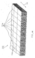
- FIG. 15 is a partial perspective view illustrating the outline of the structure of the flat layered base element obtained in the above-described manner.
- arrow 111 indicates the travel direction (circumferential direction) on the can roller 81.
- a dielectric layer 112 and a metal thin film layer 113 separated by an electrically insulating portion 114 are deposited sequentially. Thereafter, the layered base element is cut along cutting planes 115a and 115b, so that the layered product as shown in FIG. 1 can be obtained.
- the apparatus for applying patterning material in the apparatus shown in FIG. 12 is moved (to a predetermined position in the direction indicated by arrow 108 in FIG. 14 ) in the first stage or the last stage of deposition, so that the patterning material is applied in a desired deposition position of the electrically insulating band, and the can roller 81 is rotated a predetermined number of turns.
- the thickness of the resin layer and/or the metal layer can be made different from the thickness of the dielectric layer and/or the metal thin film layer simply by adjusting the rotational speed of the can roller 81 or depositing the resin layer or the metal layer by rotating a plurality of turns with shielding plates provided in the resin evaporation source 82 and /or the metal evaporation source 84.
- the can roller 81 is rotated a predetermined number of turns while the metal evaporation source 84 is shielded or metal evaporation is stopped in the first stage or the last stage of deposition, thereby depositing only the resin layer.
- the layered product is formed on the cylindrical can roller 81.
- the supporting base on which the layered product is formed is hot limited thereto, and any supporting base can be used, as long as it rotates in a vacuum apparatus.
- the layered product can be foamed on a belt-shaped supporting base that rotates around a plurality of rolls.
- the belt-shaped supporting base can be formed of a metal, a resin, a fabric or a complex of these.
- a rotating disk also can be used.
- the electrically insulating portions are formed concentrically.
- the method for producing a layered product of the present invention allows the layered product of the present invention to be produced a simple method, efficiently and inexpensively.
- a layered product was produced with the apparatus shown in FIG. 12 .
- a vacuum container 85 was evacuated to 2 ⁇ 10 -4 Torr, and the circumferential surface of the can roller 81 was maintained at 5°C.
- a portion that was to serve as a protective layer was deposited on the circumferential surface of the can roller 81.
- Dicyclopentadiene dimethanoldiacrylate was used as the material of the protective layer, and evaporated so as to be deposited on.the circumferential surface of the can roller 81.
- a UV curing device was used as the apparatus 88 for curing resin to polymerize and cure the protective layer material deposited in the above-described manner. This operation was repeated by rotating the can roller 81 so that the protective layer having a thickness of 15 ⁇ m was formed on the circumferential surface of the can roller 81.
- a portion that was to serve as a reinforcement layer was deposited.
- the same material as that for the protective layer was used as the resin layer material, and evaporated so as to be deposited on the protective layer.
- a UV curing device was used as the apparatus 88 for curing resin to polymerize and cure the resin layer material deposited in the above-described manner.
- the thickness of the thus formed resin layer was 0.6 ⁇ m.
- the surface was treated with oxygen plasma with the apparatus 89 for treating resin surface.
- a pattering material was applied with the apparatus 83 for applying pattering material.
- a fluorocarbon oil was used as the pattering material, and it was evaporated and ejected from a pinhole having a diameter of 50 ⁇ m so as to be deposited in the form of a belt having a width of 150 ⁇ m. Then, aluminum was deposited with a metal evaporation source 84. The deposition thickness was 300 ⁇ , and the film resistance was 4 ⁇ /cm 2 . Thereafter, the residual patterning material was removed by heating with a far infrared radiation heater and a plasma discharge treatment using the apparatus 87 for removing patterning material. This operation was repeated 500 times by rotating the can roller 81 so that the reinforcement layer having a total thickness of 315 ⁇ m was formed.
- the movement of the apparatus for applying patterning material in the direction perpendicular to the travel direction of the circumferential surface of the can roller 81 was performed with the device shown in FIGs. 13 and 14 in the following pattern.
- the apparatus was shifted 60 ⁇ m in a first direction; after the next rotation, the apparatus was shifted 60 ⁇ m in the same first direction; after the next rotation, it was shifted 60 ⁇ m in a second direction opposite to the first direction; and after the next rotation, it was shifted 60 ⁇ m in the second direction.
- These shifts constituted one cycle, which was repeated thereafter.
- the distance Dw between the pinholes .92 of the apparatus for applying patterning material and the deposition surface was controlled to be maintained constantly at 250 to 300 ⁇ m.
- a layered product portion comprising a dielectric layer and a metal thin film layer was deposited.
- the same material as that for the protective layer and the resin layer was used as the dielectric layer material, and evaporated so as to be deposited on the resin layer.
- a UV curing device was used as the apparatus 88 for curing resin to polymerize and cure the dielectric layer material deposited in the above-described manner.
- the thickness of the thus formed dielectric layer was 0.4 ⁇ m.
- the surface was treated with oxygen plasma with the apparatus 89 for treating resin surface.
- a pattering material was applied to a portion corresponding to an electrically insulating portion with the apparatus 83 for applying pattering material.
- a fluorocarbon oil was used as the pattering materials, and it was evaporated and ejected from a pinhole having a diameter of 50 ⁇ m so as to be deposited in the form of a belt having a width of 150 ⁇ m. Then, aluminum was deposited with a metal evaporation source 84. The deposition thickness was 300 ⁇ , and the film resistance was 4 ⁇ /cm 2 . Thereafter, the residual patterning material was removed by heating with a far infrared radiation heater and a plasma discharge treatment using the apparatus 87 for removing patterning material. This operation was repeated about 2000 times by rotating the can roller 81 so that the layered product portion having a total thickness of 860 ⁇ m was formed.
- the apparatus When the can roller 81 had rotated one turn, the apparatus was shifted 1000 ⁇ m in a first direction; after the next rotation, the apparatus was shifted 940 ⁇ m in at second direction opposite to the first direction; after the next rotation, it was shifted 1000 ⁇ m in the first direction; after the next rotation, it was shifted 940 ⁇ m in the second direction; after the next rotation, it was shifted 1000 ⁇ m in the first direction; after the next rotation, it was shifted 1060 ⁇ m in the second direction; after the next rotation, it was shifted 1000 ⁇ m in the first direction; and after the next rotation, it was shifted 1060 ⁇ m in the second direction.
- These shifts constituted one cycle, which was repeated thereafter.
- the distance Dw between the pinholes 92 of the apparatus for applying patterning material and the deposition surface was controlled to be maintained constantly at 250 to 300 ⁇ m.
- a reinforcement layer portion having a thickness of 315 ⁇ m was formed on a surface of the layered product portion.
- the method thereof was exactly the same as the method for the reinforcement layer as described above.
- a protective layer portion having a thickness of 15 ⁇ m was formed on a surface of the reinforcement layer.
- the method thereof was exactly the same as the method for the protective layer as described above.
- the obtained cylindrical layered product was cut into 8 sections in the radial direction (separated by 45°) and removed.
- the sections were pressed under heat, and flat layered base elements as shown in FIG. 15 were obtained (in reality, the reinforcement layer and the resin layer were deposited on the upper and lower surfaces).
- the flat layered base elements were cut along the cutting planes 115a, and the cutting planes were metallized with brass by spraying so as to form external electrodes.
- An electrically conducting paste where an alloy comprising copper, Ni, silver or the like had been dispersed in a thermosetting phenol resin was applied to the metallized surface, heat-cured, and the resulting resin surface was plated with molten solder. After that, the pieces were cut along the cutting planes 115b in FIG. 15 , and immersed in a silane coupling agent to coat the circumferential surface, whereby chip capacitors as shown in FIG. 11 were obtained.
- the width of the electrically insulating portion of the capacitance generation portion for a capacitor was 150 ⁇ m.
- the displacement amount dof the deposition positions of the electrically insulating portions of every other deposition unit was 60 ⁇ m.
- the maximum displacement width D of the deposition positions of the electrically insulating portions of every other deposition unit in the overall layered product was 270 ⁇ m.
- the width of the electrically insulating band of the reinforcement layer was 150 ⁇ m, and it was positioned substantially in a central portion in the width direction.
- the displacement amount d 1 of the deposition positions of the electrically insulating bands of adjacent deposition units was 60 ⁇ m.
- the maximum displacement width D 1 of the deposition positions of the electrically insulating bands in the overall reinforcement layer was 270 ⁇ m.
- the obtained chip capacitors had a thickness in the deposition direction of 1.5mm, a depth of about 1.6mm and a width (in the direction between the opposite external electrodes) of about 3.2mm, which was small, and yet the capacitance was 0.47 ⁇ F.
- the withstand voltage was 50V Irregularities on the upper and lower surfaces in the deposition direction substantially were not observed, and a difference between the uppermost point and the lowest point in the irregularities was 10 ⁇ m or less.
- the obtained chip capacitor was dismantled, and the surface roughnesses Ra of the surface of the dielectric layer and the surface of the metal thin film layer were measured, the results were 0.005 ⁇ m and 0.005 ⁇ m, respectively.
- the curing degrees of the dielectric layer, the resin layer and the protective layer were 95%, 95% and 90%, respectively.
- the conditions under which the patterning material is applied for a layered product comprising dielectric layers and metal thin film layers in Example 1 were changed as follows.
- the diameter of the pinhole of the apparatus for applying patterning material was changed to 75mm, and the patterning material was applied in the shape of a belt having a width of 200mm.
- the movement of the apparatus for applying patterning material in the direction perpendicular to the travel direction of the circumferential surface of the can roller 81 (the direction indicated by arrow 108 in FIG. 14 ) was performed with the device shown in FIGs. 13 and 14 in the following pattern.
- the apparatus When the can roller was rotated one turn, the apparatus was shifted 1000 ⁇ m in a first direction; after the next rotation, it was shifted 940 ⁇ m in a second direction opposite to the first direction; after the next rotation, it was shifted 1000 ⁇ m in the first direction; after the next rotation; it was shifted 940 ⁇ m in the second direction; after the next rotation, it was shifted 1000 ⁇ m in the first direction; after the next rotation, it was shifted 1060 ⁇ m in the second direction; after the next rotation, it was shifted 1000 ⁇ m in the first direction; and after the next rotation, it was shifted 1060 ⁇ m in the second direction.
- These shifts constituted one cycle, which was repeated thereafter.
- the layered base element shown in FIG. 16 was obtained in the same manner as in Example 1 except for the conditions described above (however, in reality, the reinforcement layer and the resin layer were deposited on the upper and lower surfaces).
- the layered base element was cut along the cutting planes 116a, and the cutting planes were metallized with brass by spraying so as to form external electrodes.
- An electrically conducting paste where an alloy comprising copper powder had been, dispersed in a thermosetting phenol resin was applied to the metallized surface, heat-cured, and the resulting resin surface was plated with molten solder. After that, the pieces were cut along the cutting planes 116b in FIG. 16 , and immersed in a silane coupling agent to coat the circumferential surface, whereby chip capacitors 70 as shown in FiG. 17 were obtained.
- the average width WAVE of the electrically insulating portion of the capacitance generation portion fora capacitor was 140 ⁇ m.
- the maximum width W MAX was 200 ⁇ m.
- the minimum width W MIN was 80 ⁇ m.
- the obtained chip capacitor had a thickness in the deposition direction of 15mm, a depth of about 1.6mm and a width (in the direction between the opposite external electrodes) of about 3.2mm, which was small, and yet the capacitance was 0.47 ⁇ F.
- the withstand voltage was 50V. Irregularities on the upper and lower surfaces in the deposition direction substantially were not observed.
- the chip capacitor was mounted onto a printed circuit board with solder, there were no problems such as the external electrodes falling off. Although the number of metal thin film layers that are connected to the external electrodes is larger than that of Example 1, sufficient adhesion strength was obtained.
- the interval between the metal thin film layers is broad, so that sprayed metal particles can penetrate between the metal thin film layers sufficiently, and the metal layer of the reinforcement layer contributes to the adhesion strength.
- the obtained chip capacitor was dismantled, and the surface roughnesses Ra of the surface of the dielectric layer and the surface of the metal thin film layer were measured, the results were 0.005 ⁇ m and 0.005 ⁇ m, respectively.
- the curing degrees of the dielectric layer, the resin layer and the protective layer were 95%, 95% and 90%, respectively.
- Chip capacitors were produced in the same manner as in Example 1, except that there was no displacement of the deposition positions of the electrically insulating portions of the layered product portion, nor displacement of the deposition positions of the electrically insulating bands of the reinforcement layer.
- the obtained chip capacitor had a thickness in the deposition direction of 1.5mm, a depth of about 1.6mm and a width (in the direction between the opposite external electrodes) of about 3.2mm.
- On the upper surface in the deposition direction there were two recesses in the electrically insulating portion of the layered product portion and one recess in the electrically insulating band of the reinforcement layer.
- the depth of the former was about 30 ⁇ m, and the depth of the latter was about 30 ⁇ m.
- the capacitance was 0.40 ⁇ F, which did not satisfy the required specification.
- the capacitance was smaller than that of Example 1, because it is estimated that the recess ins the electrically insulating portion caused a rupture in a part of the metal thin film layer.
- the withstand voltage was 16V, which did not satisfy the required specification. It is estimated that the withstand voltage was smaller than that of Example 1 because the recess in the electrically insulating band caused the thickness of the dielectric layer to become thin locally.
- the wettability of the solder was poor due to the recesses. There was no problem of the external electrodes falling off.
- a chip capacitor 70" as shown in FIG. 18 was produced under production conditions that were modified from those of Example 2.
- the production conditions were as follows.
- the movement pattern of the apparatus for applying patterning material in the direction perpendicular to the travel direction of the circumferential surface of the can roller 81 (direction indicated by arrow 108 of FIG. 14 ) was changed, and all the widths of the electrically insulating portions were the same.
- protective layers 74a and 74b are deposited directly on and below the layered product portion 72" that functions as a capacitor without providing the reinforcement layer.
- the chip capacitor was produced in the same manner as in Example 2.
- the obtained chip capacitor had a thickness in the deposition direction of 0.9mm (this was thinner that that of Example 1, because there was no reinforcement layer), a depth of about 1.6mm and a width (in the direction between the opposite external electrodes) of about 3.2mm.
- a thickness in the deposition direction of 0.9mm this was thinner that that of Example 1, because there was no reinforcement layer
- a depth of about 1.6mm and a width (in the direction between the opposite external electrodes) of about 3.2mm.
- the depth of the recess was 30 ⁇ m.
- the capacitance as a capacitor was 0.40 ⁇ F which did not satisfy the required specification.
- the thickness of the dielectric layer, the number of depositions or some other conditions were the same as those of Example 2, the capacitance was smaller than that of the capacitor of Example 2.
- the layered product of the present invention can be utilized widely for various layered products that require compactness, high performance and low cost, for example a magnetic recording medium such as a magnetic tape, a wrapping material, and an electronic component.
- the present invention can be used suitably for electronic components whose required levels have become significantly high.
- the present invention is used for a capacitor, especially as a chip capacitor, compact and high capacitance capacitors haying stable qualities can be obtained at low cost.
- the present invention is utilized to produce a chip coil, a noise filter, or other electronic components, compactness, high performance, quality stability and low cost of these electronic components can be achieved.
- the capacitor of the present invention has a similar appearance and structure to those of a conventional chip type film capacitor and yet allows compactness and high performance to higher extent than the conventional capacitor. Therefore, the present invention can be used for applications whose required specifications cannot be satisfied by the conventional chip type film capacitor.
- the method for producing the layered product of the present invention can be utilized to produce the layered product that can be used for various applications.
Landscapes
- Engineering & Computer Science (AREA)
- Power Engineering (AREA)
- Manufacturing & Machinery (AREA)
- Microelectronics & Electronic Packaging (AREA)
- Chemical & Material Sciences (AREA)
- Chemical Kinetics & Catalysis (AREA)
- Materials Engineering (AREA)
- Mechanical Engineering (AREA)
- Metallurgy (AREA)
- Organic Chemistry (AREA)
- Fixed Capacitors And Capacitor Manufacturing Machines (AREA)
Claims (17)
- Schichtprodukt (11) mit mindestens hundert Ablagerungseinheiten (15, 15a), von denen jede enthält:eine dielektrische Schicht (12, 12a) einer Dicke von nicht mehr als 1 µm, undeine erste Metall-Dünnfilm-Schicht (13, 13a) und eine zweite Metall-Dünnfilm-Schicht (14, 14a), die auf einer Oberfläche der dielektrischen Schicht abgelagert sind und voneinander durch einen gurtförmigen elektrisch isolierenden Abschnitt (16, 16a, 16b) getrennt sind,wobei die Ablagerungspositionen der elektrisch isolierenden Abschnitte (z.B. 16a, 16b) benachbarter Ablagerungseinheiten unterschiedlich sind und die Ablagerungspositionen der elektrisch isolierenden Abschnitte jeder zweiten Ablagerungseinheit über das gesamte Schichtprodukt (11) nicht dieselben sind.
- Schichtprodukt nach Anspruch 1, bei welchem die Versatzgröße der Ablagerungspositionen der elektrisch isolierenden Abschnitte (16) jeder zweiten Ablagerungseinheit mindestens W/20 und nicht mehr als 4W beträgt, wobei W eine Breite des gurtförmigen elektrisch isolierenden Abschnittes (z.B. 16b) ist.
- Schichtprodukt nach Anspruch 1, bei welchem die maximale Veränderung der Ablagerungspositionen der elektrisch isolierenden Abschnitte jeder zweiten Ablagerungseinheit mindestens 6W/5 und nicht mehr als 5W beträgt, wobei W eine Breite des gurtförmigen elektrisch isolierenden Abschnittes (z.B. 16b) ist.
- Schichtprodukt (40) mit mindestens hundert Ablagerungseinheiten (44), von denen jeder enthält:eine dielektrische Schicht (41, 41a) einer Dicke von nicht mehr als 1 µm undeine Metall-Dünnfilm-Schicht (42, 42a), die auf einer Oberfläche der dielektrischen Schicht (41, 41a) mit Ausnahme eines Abschnittes abgelagert ist, wo sich ein gurtförmiger elektrisch isolierender Abschnitt (43, 43a, 43b) an einem Ende der Oberfläche der dielektrischen Schicht (41, 41a) befindet,wobei die elektrisch isolierenden Abschnitte (43, 43a) benachbarter Ablagerungseinheiten auf gegenüberliegenden Seiten liegen und
die Breiten der elektrisch isolierenden Abschnitte jeder zweiten Ablagerungseinheit über das gesamte Ablagerungsprodukt nicht dieselben sind. - Schichtprodukt nach Anspruch 4, bei welchem (W MAX - W MIN) / W AVE mindestens W AVE/5 x die Längseinheit und nicht mehr als W AVE/1 x die Längseinheit ist, wobei W AVE die mittlere Breite der elektrisch isolierenden Abschnitte jeder zweiten Ablagerungseinheit und W MAX ein Maximum hiervon und W MIN ein Minimum hiervon ist.
- Schichtprodukt nach Anspruch 1 oder 4, bei welchem auf mindestens einer Oberfläche des Schichtproduktes (11) eine Verstärkungsschicht (50a, 50b) abgelagert ist und
diese Verstärkungsschicht (50a, 50b) mindestens eine Ablagerungseinheit (54) umfasst, und die Einheit eine Kunstharzschicht (51), eine erste Metallschicht (52) und eine zweite Metallschicht (53) umfasst, welche auf einer Oberfläche der Kunstharzschicht (51) abgelagert sind und durch ein elektrisch isolierendes Band (55) voneinander getrennt sind. - Schichtprodukt nach Anspruch 6, bei welchem das elektrisch isolierende Band (55) im Wesentlichen in einem zentralen Abschnitt des Schichtproduktes positioniert ist.
- Schichtprodukt nach Anspruch 6, bei welchem die Verstärkungsschicht (50a, 50b) mindestens zwei Ablagerungseinheiten umfasst und
die Ablagerungspositionen der elektrisch isolierenden Bänder über die gesamte Verstärkungsschicht (50a, 50b) nicht die gleichen sind. - Schichtprodukt nach Anspruch 8, bei welchem das elektrisch isolierende Band (55) die Form eines Gurtes konstanter Breite W1 hat, und
die Ablagerungspositionen der elektrisch isolierenden Bändern benachbarter Ablagerungseinheiten um mindestens W1/20 versetzt sind. - Schichtprodukt nach Anspruch 6, bei welchem die Verstärkungsschicht (50a, 50b) mindestens zwei Ablagerungseinheiten umfasst,
und das elektrisch isolierende Band (55) die Form eines Gurtes konstanter Breite (W1) hat und
die maximale Abweichung der Ablagerungspositionen der elektrisch isolierenden Bänder über die gesamte Verstärkungsschicht mindestens 6W1/5 beträgt. - Schichtprodukt nach Anspruch 1 oder 4, bei welchem auf mindestens einer Oberfläche des Schichtproduktes eine Verstärkungsschicht (60a, 60b) abgelagert ist,
und die Verstärkungsschicht (60a, 60b) mindestens eine Ablagerungseinheit (64) umfasst, welche ihrerseits eine Kunstharzschicht (61) und eine Metallschicht (62) aufweist, die auf einer Oberfläche der Kunstharzschicht mit Ausnahme eines Abschnittes abgelagert ist, wo sich ein gurtförmiges elektrisch isolierendes Band (63) an einem Ende der Oberfläche der Kunstharzschicht (61) befindet. - Schichtprodukt nach Anspruch 11, bei welchem die Verstärkungsschicht (60a, 60b) mindestens zwei Ablagerungseinheiten umfasst und
die Breiten der elektrisch isolierenden Bänder über die gesamte Verstärkungsschicht (60a, 60b) nicht dieselben sind. - Schichtprodukt nach Anspruch 11, bei dem (W1 MAX - W1 MIN)/W1 AVE mindestens W1 AVE/5 x die Längeneinheit ist, wobei W1 AVE eine mittlere Breite der elektrisch isolierenden Bänder, W1 MAX davon das Maximum und W1 MIN davon das Minimum ist.
- Kondensator, der mit dem Schichtprodukt (11) nach den Ansprüchen 1 oder 4 gebildet ist.
- Verfahren zur Herstellung eines Schichtproduktes mit den Schritten:Wiederholung einer Prozesseinheit für eine vorbestimmte Anzahl von Malen, wobei die Prozesseinheit enthält:Verwendung eines Kunstharzmaterials zur Ablagerung einer dielektrischen Schicht,Aufbringen eines Schablonenmaterials in Gurtform auf die dielektrische Schicht undAblagerung einer Metall-Dünnfilm-Schicht,so dass ein Schichtprodukt mit dielektrischen Schichten und Metall-Dünnfilm-Schichten gebildet wird, wobei eine Position der 2nten (n ist eine natürliche Zahl) Aufbringung des Schablonenmaterials verschieden von derjenigen der 2 (n-1)ten Aufbringung ist undalle die Positionen der 2nten Aufbringung des Schablonenmaterials nicht dieselben sind undalle Positionen der 2 (n-1)ten Aufbringungen des Schablonenmaterials nicht dieselben sind.
- Verfahren zur Herstellung eines Schichtprodukts nach Anspruch 15,
wobei eine Position der 2 (n+1)ten Aufbringung des Schablonenmaterials bezüglich der Position des 2 (n-1)ten Aufbringung des Schablonenmaterials um W/20 bis 4W versetzt ist, wobei W die Aufbringungsbreite des gurtförmigen Schablonenmaterials ist, und
eine Position der 2 (n+2)ten Aufbringung des Schablonenmaterials bezüglich der Position der 2nten Aufbringung des Schablonenmaterials um W/20 bis 4W versetzt ist. - Verfahren zur Herstellung eines Schichtprodukts nach Anspruch 15, wobei ein Maximum der Variationen der Positionen der 2nten Aufbringung des Schablonenmaterials und ein Maximum der Variationen der Positionen der 2 (n-1)ten Aufbringung des Schablonenmaterials 6W/5 bis 5W beträgt, wobei W eine Aufbringungsbreite des gurtförmigen Schablonenmaterials ist.
Applications Claiming Priority (3)
| Application Number | Priority Date | Filing Date | Title |
|---|---|---|---|
| JP31741697A JP3630357B2 (ja) | 1997-11-18 | 1997-11-18 | 積層体の製造方法 |
| JP31741297A JP3391677B2 (ja) | 1997-11-18 | 1997-11-18 | 積層体及びコンデンサ |
| EP98953068A EP1035553B1 (de) | 1997-11-18 | 1998-11-16 | Verfahren zur herstellung von laminat |
Related Parent Applications (2)
| Application Number | Title | Priority Date | Filing Date |
|---|---|---|---|
| EP98953068A Division EP1035553B1 (de) | 1997-11-18 | 1998-11-16 | Verfahren zur herstellung von laminat |
| EP98953068.8 Division | 1998-11-16 |
Publications (2)
| Publication Number | Publication Date |
|---|---|
| EP1732091A1 EP1732091A1 (de) | 2006-12-13 |
| EP1732091B1 true EP1732091B1 (de) | 2009-10-07 |
Family
ID=26569008
Family Applications (2)
| Application Number | Title | Priority Date | Filing Date |
|---|---|---|---|
| EP98953068A Expired - Lifetime EP1035553B1 (de) | 1997-11-18 | 1998-11-16 | Verfahren zur herstellung von laminat |
| EP06017841A Expired - Lifetime EP1732091B1 (de) | 1997-11-18 | 1998-11-16 | Mehrschichtprodukt, Kondensator und Verfahren zur Herstellung des Mehrschichtprodukts |
Family Applications Before (1)
| Application Number | Title | Priority Date | Filing Date |
|---|---|---|---|
| EP98953068A Expired - Lifetime EP1035553B1 (de) | 1997-11-18 | 1998-11-16 | Verfahren zur herstellung von laminat |
Country Status (6)
| Country | Link |
|---|---|
| US (2) | US6576523B1 (de) |
| EP (2) | EP1035553B1 (de) |
| KR (1) | KR100372863B1 (de) |
| CN (2) | CN1158682C (de) |
| DE (2) | DE69841227D1 (de) |
| WO (1) | WO1999026259A1 (de) |
Cited By (1)
| Publication number | Priority date | Publication date | Assignee | Title |
|---|---|---|---|---|
| DE112013001679B4 (de) | 2012-03-26 | 2023-03-09 | Kemet Electronics Corporation | Asymmetrischer Hochspannungskondensator |
Families Citing this family (26)
| Publication number | Priority date | Publication date | Assignee | Title |
|---|---|---|---|---|
| DE69841227D1 (de) * | 1997-11-18 | 2009-11-19 | Panasonic Corp | Mehrschichtprodukt, Kondensator und Verfahren zur Herstellung des Mehrschichtprodukts |
| JP4533504B2 (ja) * | 2000-04-28 | 2010-09-01 | パナソニック株式会社 | 電子部品の製造方法 |
| DE10026259A1 (de) * | 2000-05-26 | 2001-12-06 | Epcos Ag | Kondensator und Verfahren zur Herstellung des Kondensators |
| JP4680380B2 (ja) * | 2000-12-26 | 2011-05-11 | 株式会社リケン | ピストンリング及びその製造方法 |
| US7152291B2 (en) | 2002-04-15 | 2006-12-26 | Avx Corporation | Method for forming plated terminations |
| JP2003332169A (ja) * | 2002-05-15 | 2003-11-21 | Matsushita Electric Ind Co Ltd | 積層コンデンサ及びその製造方法 |
| DE10330401B3 (de) * | 2003-07-04 | 2005-02-24 | Applied Films Gmbh & Co. Kg | Verfahren und Vorrichtung zum bereichsweisen Auftragen von Trennmitteln |
| JP4964408B2 (ja) * | 2003-07-14 | 2012-06-27 | フレックス プロダクツ インコーポレイテッド | 顕在的および/または隠在的パターン化層を有する真空ロール被覆偽造防止薄膜干渉品 |
| CA2542819A1 (en) * | 2003-09-30 | 2005-04-07 | Japan Science And Technology Agency | Metal thin film chip production method and metal thin film chip production device |
| DE102005018984A1 (de) * | 2005-04-22 | 2006-11-02 | Steiner Gmbh & Co. Kg | Verfahren und Vorrichtung zum Herstellen von elektronischen Bauteilen |
| USD547720S1 (en) * | 2005-05-12 | 2007-07-31 | Honda Motor Co., Ltd. | Capacitor cell |
| JP4934325B2 (ja) * | 2006-02-17 | 2012-05-16 | 株式会社フジクラ | プリント配線板の接続構造及びプリント配線板の接続方法 |
| DE102007031457A1 (de) | 2007-07-05 | 2009-01-08 | Leybold Optics Gmbh | Verfahren und Vorrichtung zur Aufbringung einer Schicht eines Trennmittels auf ein Substrat |
| US8482048B2 (en) * | 2009-07-31 | 2013-07-09 | Alpha & Omega Semiconductor, Inc. | Metal oxide semiconductor field effect transistor integrating a capacitor |
| JP4511625B1 (ja) * | 2009-10-16 | 2010-07-28 | ルビコン株式会社 | 積層コンデンサ、その製造方法、回路基板および電子機器 |
| JP5603201B2 (ja) * | 2010-10-27 | 2014-10-08 | サントリーホールディングス株式会社 | 樹脂製容器の表面改質方法および樹脂製容器の表面改質装置 |
| JP5770539B2 (ja) * | 2011-06-09 | 2015-08-26 | Tdk株式会社 | 電子部品及び電子部品の製造方法 |
| JP2013058558A (ja) | 2011-09-07 | 2013-03-28 | Tdk Corp | 電子部品 |
| TWI621143B (zh) * | 2016-08-10 | 2018-04-11 | 鈺邦科技股份有限公司 | 薄膜電容器及其製作方法 |
| TWI665692B (zh) * | 2017-08-11 | 2019-07-11 | 鈺邦科技股份有限公司 | 多層式堆疊結構的製作設備以及薄膜電容器的製作方法 |
| TWI641009B (zh) * | 2017-10-13 | 2018-11-11 | 鈺邦科技股份有限公司 | 多層式堆疊結構的製作設備以及薄膜電容器的製作方法 |
| JP7551280B2 (ja) * | 2018-07-24 | 2024-09-17 | Tdk株式会社 | 積層セラミック電子部品 |
| KR102127804B1 (ko) * | 2018-11-07 | 2020-06-29 | 삼성전기주식회사 | 적층 세라믹 전자부품 |
| CN110600283B (zh) * | 2019-09-03 | 2021-08-03 | 黄山申格电子科技股份有限公司 | 电容器气相沉积负压镀金装置及其镀金方法 |
| JP2022021734A (ja) * | 2020-07-22 | 2022-02-03 | 太陽誘電株式会社 | セラミック電子部品およびその製造方法 |
| US11854748B2 (en) * | 2021-11-26 | 2023-12-26 | Rubycon Corporation | Thin film high polymer laminated capacitor manufacturing method |
Family Cites Families (50)
| Publication number | Priority date | Publication date | Assignee | Title |
|---|---|---|---|---|
| US3617834A (en) * | 1970-08-31 | 1971-11-02 | Illinois Tool Works | Monolithic capacitor components and process for producing same |
| DE2837723A1 (de) | 1978-08-30 | 1980-03-13 | Walter Krause | Schlammfilter |
| JPS5579867A (en) * | 1978-12-11 | 1980-06-16 | Honshu Paper Co Ltd | Vacuum evaporation method |
| US4349862A (en) * | 1980-08-11 | 1982-09-14 | International Business Machines Corporation | Capacitive chip carrier and multilayer ceramic capacitors |
| JPS6050053B2 (ja) * | 1980-11-28 | 1985-11-06 | 日本真空技術株式会社 | オイルマスク装置 |
| EP0117258B1 (de) * | 1983-02-23 | 1987-05-20 | Ibm Deutschland Gmbh | Verfahren zur Herstellung von haftfesten Metallschichten auf Kunststoffsubstraten |
| JPS6050053A (ja) | 1983-08-31 | 1985-03-19 | Nissan Motor Co Ltd | 車両用盗難防止装置 |
| US5032461A (en) | 1983-12-19 | 1991-07-16 | Spectrum Control, Inc. | Method of making a multi-layered article |
| US5125138A (en) | 1983-12-19 | 1992-06-30 | Spectrum Control, Inc. | Miniaturized monolithic multi-layer capacitor and apparatus and method for making same |
| DE3484793D1 (de) | 1983-12-19 | 1991-08-14 | Spectrum Control Inc | Miniaturisierter monolithischer mehrschichtkondensator sowie geraet und verfahren zur herstellung. |
| US4622058A (en) * | 1984-06-22 | 1986-11-11 | International Business Machines Corporation | Formation of a multi-layer glass-metallized structure formed on and interconnected to multi-layered-metallized ceramic substrate |
| JPS6142903A (ja) | 1984-08-06 | 1986-03-01 | 株式会社村田製作所 | 電子部品の外装材の形成方法 |
| JPS61183913A (ja) * | 1985-02-08 | 1986-08-16 | 株式会社村田製作所 | 積層コンデンサ |
| JPH0414450Y2 (de) * | 1986-03-14 | 1992-03-31 | ||
| JPS6331570A (ja) | 1986-07-23 | 1988-02-10 | Toray Ind Inc | 走行ウエブの塗装方法 |
| JPS6331929A (ja) | 1986-07-25 | 1988-02-10 | Toshiba Corp | 部品の間歇供給装置 |
| JPS6370411A (ja) * | 1986-09-11 | 1988-03-30 | 松下電器産業株式会社 | 金属化フイルムの製造方法 |
| US5037691A (en) * | 1986-09-15 | 1991-08-06 | Compositech, Ltd. | Reinforced plastic laminates for use in the production of printed circuit boards and process for making such laminates and resulting products |
| US5171718A (en) * | 1987-11-27 | 1992-12-15 | Sony Corporation | Method for forming a fine pattern by using a patterned resist layer |
| JPH0611018B2 (ja) * | 1988-01-07 | 1994-02-09 | 株式会社村田製作所 | セラミック生シートの積層方法 |
| JPH0817143B2 (ja) * | 1988-03-30 | 1996-02-21 | 松下電器産業株式会社 | フィルムコンデンサとその製造方法 |
| EP0339844A3 (de) | 1988-04-29 | 1991-01-16 | SPECTRUM CONTROL, INC. (a Delaware corporation) | Mehrschichtstruktur und Verfahren zu deren Herstellung |
| US5290606A (en) * | 1989-01-30 | 1994-03-01 | Svein Hestevik | Method for manufacturing a substrate for a printed circuit board |
| JPH0650701B2 (ja) * | 1989-05-18 | 1994-06-29 | 松下電器産業株式会社 | 積層コンデンサ素子とその製造方法 |
| JPH0793238B2 (ja) | 1989-06-30 | 1995-10-09 | 松下電器産業株式会社 | フィルムコンデンサの製造方法 |
| JPH10135634A (ja) * | 1990-03-19 | 1998-05-22 | Hitachi Ltd | 多層配線基板及びその製造方法 |
| JP3022582B2 (ja) | 1990-05-09 | 2000-03-21 | シーアイ化成株式会社 | 化粧フィルムとその製造方法 |
| JPH0499164A (ja) * | 1990-08-03 | 1992-03-31 | Matsushita Electric Ind Co Ltd | オイルマスク用蒸発器 |
| US5214844A (en) * | 1990-12-17 | 1993-06-01 | Nchip, Inc. | Method of assembling integrated circuits to a silicon board |
| DE4100643C1 (de) * | 1991-01-11 | 1991-10-31 | Leybold Ag, 6450 Hanau, De | |
| EP0507113B1 (de) | 1991-04-05 | 1995-08-30 | Balzers Aktiengesellschaft | Verfahren zur Beschichtung eines Werkstückes aus Kunststoff mit einer Metallschicht |
| US5153813A (en) * | 1991-10-31 | 1992-10-06 | International Business Machines Corporation | High area capacitor formation using dry etching |
| JP3088179B2 (ja) | 1992-03-17 | 2000-09-18 | 松下電器産業株式会社 | 積層薄膜コンデンサの製造方法 |
| JP2914098B2 (ja) * | 1993-06-29 | 1999-06-28 | 東レ株式会社 | 蒸着フィルムの測定、制御方法、装置および製造方法 |
| EP0701277B1 (de) * | 1994-05-27 | 2008-02-27 | Texas Instruments Incorporated | Verbindungsverfahren mit Benutzung eines porösen Isolators zur Reduzierung der Kapazitäten zwischen Leiterbahnen |
| US5917157A (en) * | 1994-12-12 | 1999-06-29 | Remsburg; Ralph | Multilayer wiring board laminate with enhanced thermal dissipation to dielectric substrate laminate |
| US5583359A (en) * | 1995-03-03 | 1996-12-10 | Northern Telecom Limited | Capacitor structure for an integrated circuit |
| DE19527604A1 (de) * | 1995-07-28 | 1997-01-30 | Leybold Ag | Verfahren und Vorrichtung zur Herstellung von metallfreien Streifen bei der Metallbedampfung |
| US5623160A (en) * | 1995-09-14 | 1997-04-22 | Liberkowski; Janusz B. | Signal-routing or interconnect substrate, structure and apparatus |
| JP3374627B2 (ja) * | 1995-12-05 | 2003-02-10 | 東レ株式会社 | ポリエステルフィルムおよびその製造方法 |
| JP3316731B2 (ja) * | 1996-01-11 | 2002-08-19 | 株式会社村田製作所 | 積層セラミック電子部品 |
| US5946566A (en) * | 1996-03-01 | 1999-08-31 | Ace Memory, Inc. | Method of making a smaller geometry high capacity stacked DRAM device |
| US5759737A (en) * | 1996-09-06 | 1998-06-02 | International Business Machines Corporation | Method of making a component carrier |
| US5898215A (en) * | 1996-12-16 | 1999-04-27 | Motorola, Inc. | Microelectronic assembly with connection to a buried electrical element, and method for forming same |
| SE520173C2 (sv) * | 1997-04-29 | 2003-06-03 | Ericsson Telefon Ab L M | Förfarande för tillverkning av en kondensator i en integrerad krets |
| US5856068A (en) * | 1997-05-02 | 1999-01-05 | Motorola, Inc. | Method for fabricating a printed circuit board by curing under superatmospheric pressure |
| US5945203A (en) * | 1997-10-14 | 1999-08-31 | Zms Llc | Stratified composite dielectric and method of fabrication |
| DE69841227D1 (de) * | 1997-11-18 | 2009-11-19 | Panasonic Corp | Mehrschichtprodukt, Kondensator und Verfahren zur Herstellung des Mehrschichtprodukts |
| EP1017101B1 (de) * | 1998-12-29 | 2009-07-29 | Nxp B.V. | Integrierter Schaltkreis mit einem Kapazitätsnetzwerk mit niedriger Dispersion |
| US6236572B1 (en) * | 1999-02-04 | 2001-05-22 | Dell Usa, L.P. | Controlled impedance bus and method for a computer system |
-
1998
- 1998-11-16 DE DE69841227T patent/DE69841227D1/de not_active Expired - Lifetime
- 1998-11-16 US US09/554,161 patent/US6576523B1/en not_active Expired - Lifetime
- 1998-11-16 DE DE69836762T patent/DE69836762T2/de not_active Expired - Lifetime
- 1998-11-16 CN CNB988130815A patent/CN1158682C/zh not_active Expired - Fee Related
- 1998-11-16 KR KR10-2000-7005397A patent/KR100372863B1/ko not_active Expired - Fee Related
- 1998-11-16 EP EP98953068A patent/EP1035553B1/de not_active Expired - Lifetime
- 1998-11-16 EP EP06017841A patent/EP1732091B1/de not_active Expired - Lifetime
- 1998-11-16 WO PCT/JP1998/005154 patent/WO1999026259A1/ja not_active Ceased
- 1998-11-16 CN CNB2004100018586A patent/CN1257053C/zh not_active Expired - Fee Related
-
2002
- 2002-12-06 US US10/313,227 patent/US6838153B2/en not_active Expired - Fee Related
Cited By (1)
| Publication number | Priority date | Publication date | Assignee | Title |
|---|---|---|---|---|
| DE112013001679B4 (de) | 2012-03-26 | 2023-03-09 | Kemet Electronics Corporation | Asymmetrischer Hochspannungskondensator |
Also Published As
| Publication number | Publication date |
|---|---|
| CN1257053C (zh) | 2006-05-24 |
| KR20010032207A (ko) | 2001-04-16 |
| CN1158682C (zh) | 2004-07-21 |
| EP1732091A1 (de) | 2006-12-13 |
| CN1285952A (zh) | 2001-02-28 |
| US20030087037A1 (en) | 2003-05-08 |
| WO1999026259A1 (en) | 1999-05-27 |
| KR100372863B1 (ko) | 2003-02-19 |
| EP1035553A4 (de) | 2005-10-12 |
| US6576523B1 (en) | 2003-06-10 |
| DE69836762D1 (de) | 2007-02-08 |
| CN1533881A (zh) | 2004-10-06 |
| DE69841227D1 (de) | 2009-11-19 |
| US6838153B2 (en) | 2005-01-04 |
| EP1035553B1 (de) | 2006-12-27 |
| EP1035553A1 (de) | 2000-09-13 |
| DE69836762T2 (de) | 2007-10-11 |
Similar Documents
| Publication | Publication Date | Title |
|---|---|---|
| EP1732091B1 (de) | Mehrschichtprodukt, Kondensator und Verfahren zur Herstellung des Mehrschichtprodukts | |
| US6577493B2 (en) | Layered product and capacitor | |
| US6106627A (en) | Apparatus for producing metal coated polymers | |
| US5125138A (en) | Miniaturized monolithic multi-layer capacitor and apparatus and method for making same | |
| US5304274A (en) | Method for manufacturing electrodes for multilayer ceramic capacitors | |
| EP0938971B1 (de) | Verfahren zur Herstellung eines Mehrschichtstoffes | |
| US3855507A (en) | Self heating capacitors | |
| US5179773A (en) | Process of manufacturing multilayer ceramic capacitors | |
| JP3391677B2 (ja) | 積層体及びコンデンサ | |
| EP0339844A2 (de) | Mehrschichtstruktur und Verfahren zu deren Herstellung | |
| EP0966006B1 (de) | Herstellungsverfahren von einem Kondensator | |
| JP3484333B2 (ja) | 積層体及びコンデンサ | |
| CN1184347C (zh) | 薄膜的制造方法及制造装置 | |
| JP2003178929A (ja) | 積層体の製造方法 | |
| JPH11147279A (ja) | 積層体及びコンデンサ | |
| JPS6386413A (ja) | コンデンサ用薄膜誘電体材料の製造方法 |
Legal Events
| Date | Code | Title | Description |
|---|---|---|---|
| PUAI | Public reference made under article 153(3) epc to a published international application that has entered the european phase |
Free format text: ORIGINAL CODE: 0009012 |
|
| 17P | Request for examination filed |
Effective date: 20060826 |
|
| AC | Divisional application: reference to earlier application |
Ref document number: 1035553 Country of ref document: EP Kind code of ref document: P |
|
| AK | Designated contracting states |
Kind code of ref document: A1 Designated state(s): DE GB NL |
|
| 17Q | First examination report despatched |
Effective date: 20070301 |
|
| AKX | Designation fees paid |
Designated state(s): DE GB NL |
|
| RAP1 | Party data changed (applicant data changed or rights of an application transferred) |
Owner name: PANASONIC CORPORATION |
|
| RTI1 | Title (correction) |
Free format text: LAYERED PRODUCT, CAPACITOR AND A METHOD FOR PRODUCING THE LAYERED PRODUCT |
|
| GRAP | Despatch of communication of intention to grant a patent |
Free format text: ORIGINAL CODE: EPIDOSNIGR1 |
|
| RIN1 | Information on inventor provided before grant (corrected) |
Inventor name: SUZAWA, SHINICHI Inventor name: SUNAGARE, NOBUKI Inventor name: ODAGIRI, MASARU Inventor name: ENCHIGO, NORIYASU Inventor name: HONDA, KAZUYOSHI |
|
| GRAS | Grant fee paid |
Free format text: ORIGINAL CODE: EPIDOSNIGR3 |
|
| GRAA | (expected) grant |
Free format text: ORIGINAL CODE: 0009210 |
|
| RIN1 | Information on inventor provided before grant (corrected) |
Inventor name: SUZAWA, SHINICHI Inventor name: ODAGIRI, MASARU Inventor name: ECHIGO, NORIYASU Inventor name: SUNAGARE, NOBUKI Inventor name: HONDA, KAZUYOSHI |
|
| AC | Divisional application: reference to earlier application |
Ref document number: 1035553 Country of ref document: EP Kind code of ref document: P |
|
| AK | Designated contracting states |
Kind code of ref document: B1 Designated state(s): DE GB NL |
|
| REG | Reference to a national code |
Ref country code: GB Ref legal event code: FG4D |
|
| REF | Corresponds to: |
Ref document number: 69841227 Country of ref document: DE Date of ref document: 20091119 Kind code of ref document: P |
|
| PLBE | No opposition filed within time limit |
Free format text: ORIGINAL CODE: 0009261 |
|
| STAA | Information on the status of an ep patent application or granted ep patent |
Free format text: STATUS: NO OPPOSITION FILED WITHIN TIME LIMIT |
|
| 26N | No opposition filed |
Effective date: 20100708 |
|
| GBPC | Gb: european patent ceased through non-payment of renewal fee |
Effective date: 20100107 |
|
| PG25 | Lapsed in a contracting state [announced via postgrant information from national office to epo] |
Ref country code: GB Free format text: LAPSE BECAUSE OF NON-PAYMENT OF DUE FEES Effective date: 20100107 |
|
| PGFP | Annual fee paid to national office [announced via postgrant information from national office to epo] |
Ref country code: DE Payment date: 20131113 Year of fee payment: 16 |
|
| PGFP | Annual fee paid to national office [announced via postgrant information from national office to epo] |
Ref country code: NL Payment date: 20131010 Year of fee payment: 16 |
|
| REG | Reference to a national code |
Ref country code: DE Ref legal event code: R119 Ref document number: 69841227 Country of ref document: DE |
|
| REG | Reference to a national code |
Ref country code: NL Ref legal event code: V1 Effective date: 20150601 |
|
| PG25 | Lapsed in a contracting state [announced via postgrant information from national office to epo] |
Ref country code: NL Free format text: LAPSE BECAUSE OF NON-PAYMENT OF DUE FEES Effective date: 20150601 |
|
| PG25 | Lapsed in a contracting state [announced via postgrant information from national office to epo] |
Ref country code: DE Free format text: LAPSE BECAUSE OF NON-PAYMENT OF DUE FEES Effective date: 20150602 |