EP1020923A2 - Transistor bipolaire vertical et méthode pour sa fabrication - Google Patents
Transistor bipolaire vertical et méthode pour sa fabrication Download PDFInfo
- Publication number
- EP1020923A2 EP1020923A2 EP00100084A EP00100084A EP1020923A2 EP 1020923 A2 EP1020923 A2 EP 1020923A2 EP 00100084 A EP00100084 A EP 00100084A EP 00100084 A EP00100084 A EP 00100084A EP 1020923 A2 EP1020923 A2 EP 1020923A2
- Authority
- EP
- European Patent Office
- Prior art keywords
- semiconductor layer
- opening
- insulating film
- single crystal
- semiconductor
- Prior art date
- Legal status (The legal status is an assumption and is not a legal conclusion. Google has not performed a legal analysis and makes no representation as to the accuracy of the status listed.)
- Withdrawn
Links
Images


Classifications
-
- H—ELECTRICITY
- H10—SEMICONDUCTOR DEVICES; ELECTRIC SOLID-STATE DEVICES NOT OTHERWISE PROVIDED FOR
- H10D—INORGANIC ELECTRIC SEMICONDUCTOR DEVICES
- H10D48/00—Individual devices not covered by groups H10D1/00 - H10D44/00
- H10D48/30—Devices controlled by electric currents or voltages
- H10D48/32—Devices controlled by only the electric current supplied, or only the electric potential applied, to an electrode which does not carry the current to be rectified, amplified or switched
- H10D48/34—Bipolar devices
-
- H—ELECTRICITY
- H10—SEMICONDUCTOR DEVICES; ELECTRIC SOLID-STATE DEVICES NOT OTHERWISE PROVIDED FOR
- H10D—INORGANIC ELECTRIC SEMICONDUCTOR DEVICES
- H10D10/00—Bipolar junction transistors [BJT]
- H10D10/01—Manufacture or treatment
- H10D10/051—Manufacture or treatment of vertical BJTs
- H10D10/054—Forming extrinsic base regions on silicon substrate after insulating device isolation in vertical BJTs having single crystalline emitter, collector or base regions
-
- H—ELECTRICITY
- H10—SEMICONDUCTOR DEVICES; ELECTRIC SOLID-STATE DEVICES NOT OTHERWISE PROVIDED FOR
- H10D—INORGANIC ELECTRIC SEMICONDUCTOR DEVICES
- H10D10/00—Bipolar junction transistors [BJT]
- H10D10/01—Manufacture or treatment
- H10D10/021—Manufacture or treatment of heterojunction BJTs [HBT]
-
- H—ELECTRICITY
- H10—SEMICONDUCTOR DEVICES; ELECTRIC SOLID-STATE DEVICES NOT OTHERWISE PROVIDED FOR
- H10D—INORGANIC ELECTRIC SEMICONDUCTOR DEVICES
- H10D10/00—Bipolar junction transistors [BJT]
- H10D10/40—Vertical BJTs
- H10D10/421—Vertical BJTs having both emitter-base and base-collector junctions ending at the same surface of the body
-
- H—ELECTRICITY
- H10—SEMICONDUCTOR DEVICES; ELECTRIC SOLID-STATE DEVICES NOT OTHERWISE PROVIDED FOR
- H10D—INORGANIC ELECTRIC SEMICONDUCTOR DEVICES
- H10D30/00—Field-effect transistors [FET]
- H10D30/01—Manufacture or treatment
- H10D30/051—Manufacture or treatment of FETs having PN junction gates
- H10D30/0512—Manufacture or treatment of FETs having PN junction gates of FETs having PN homojunction gates
Definitions
- the present invention relates generally to a semiconductor device and a method of manufacturing the semiconductor device, and more particularly to a transistor such as a vertical bipolar transistor, a field effect transistor or the like and its manufacturing method in which variation of electrical characteristic can be remarkably suppressed.
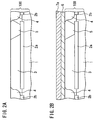
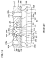
- FIG. 16 is a rough sectional view of a conventional vertical bipolar transistor similar to the vertical bipolar transistor disclosed in Japanese Patent No.2,551,353.
- reference number 1 shows a p-type silicon substrate which has a surface of (100) plane and an electrical resistivity of 10 to 20 ⁇ cm.
- Two kinds of buried layers of a few micrometers in thickness are formed on the surface area of this silicon substrate 1.
- the two kinds of buried layers are an n+ type buried layer 202a and a channel stopper p+ type buried layer 202b, which exist separately from each other.
- a collector n- type epitaxial silicon layer 203 is formed on the surfaces of these buried layers and on the surface of an area of the silicon substrate 201where these buried layers do not exist.
- a silicon oxide film 204 is selectively formed to the depth reaching the p+ type buried layer 202b, and the silicon oxide film 204 forms an element isolation film.
- an n+ type collector lead-out region 205 connected to the n+ type buried layer 202a is formed by doping impurities in high concentration into a part of the collector n- type epitaxial silicon layer 203. The portions described so far are collectively called a silicon basic body 200.
- a silicon oxide film 206 is formed on the silicon basic body 200, and a base electrode p+ type polysilicon film 207 is selectively formed on the silicon oxide film 206. And the base electrode polysilicon film 207 is covered with a silicon nitride film 208. An opening 301 is formed so as to penetrate the silicon nitride film 208 and the base electrode p+ type polysilicon film 207, and an opening 302 is formed so as to penetrate the silicon oxide film 206. A collector epitaxial silicon layer 203 is partially exposed by these openings. This first opening 301 formed in the polysilicon film 207 is projected horizontally over the opening 302 from the edge of the second opening 302. That is to say, the width of the second opening 302 is larger than the width of the first opening 301.
- a p+ type single crystal silicon intrinsic base 211 is formed on the collector epitaxial silicon layer 203 which is exposed by the second opening 302.
- a p+ type polysilicon film 212 is formed on the side surface and the exposed lower surface of the base electrode polysilicon film 207.
- the p+ type polysilicon film 212 connects the base electrode polysilicon film 207 and the intrinsic base 211 to each other.
- An n++ type single crystal silicon emitter region 215 is provided in the middle area on the p+ type single crystal silicon intrinsic base 211.
- a silicon oxide film 213 is formed so as to cover the side wall of the opening.
- an n type silicon collector region 214 in which the concentration of impurities is higher than that of impurities in the original collector epitaxial silicon layer 203.
- An emitter electrode n++ type polysilicon 216 is provided on the n++ type single crystal silicon emitter region 215. These regions are all covered with a silicon oxide film 217.
- contact holes 303a, 303b and 303c which penetrate the silicon oxide film 217 and, depending upon places, penetrates also the silicon nitride film 208 and the silicon oxide film 206 are formed.
- a metal film of aluminum-based alloy and the like is formed so as to fill these contact holes 303a, 303b and 303c, and furthermore a patterning process is applied to this metal film to form an emitter electrode 218a, a base electrode 218b and a collector electrode 218c.
- These emitter electrode 218a, base electrode 218b and collector electrode 218c composed of aluminum-based alloy are respectively in contact with the emitter electrode polysilicon 216, base electrode polysilicon film 207 and collector lead-out region 205.
- a vertical bipolar transistor of the above-mentioned configuration shown in Fig. 16 has an adequate high-speed operation characteristic, but has a problem of large variation or dispersion in an operating current. Concretely speaking, it can be explained as follows.
- a bipolar transistor circuit a differential transistor pair is formed by short-circuiting with each other the emitters of adjacent transistors. It is assumed that voltages to be applied to the bases so that the collector currents of the respective transistors of the differential transistor pair become equal to each other are respectively VB1 and VB2. If the absolute value of the difference between these voltages, namely, the absolute value of "VB1 - VB2" is defined as ⁇ VB, the smaller this ⁇ VB is, the more stable the circuit operation becomes.
- a vertical type bipolar transistor of the above-mentioned configuration shown in Fig. 16 has a large value of this ⁇ VB.
- the film thickness W H of an intrinsic base single crystal film formed by a selective crystal growth method can be made thicker than the spacing W I between the upper surface of the collector epitaxial silicon layer and the lower surface of the base electrode polysilicon film (W H > W I ).
- W H > W I the spacing between the upper surface of the collector epitaxial silicon layer and the lower surface of the base electrode polysilicon film
- an object of the present invention is to provide a semiconductor device and its manufacturing method which can solve the above-mentioned problems in the prior art.
- a semiconductor device comprising: a single crystal semiconductor substrate of a first conductivity type; a first insulating film which is formed on the main surface of said single crystal semiconductor substrate and which has a first opening having a first width to expose a portion of said main surface of said single crystal semiconductor substrate; a first semiconductor layer formed on at least a portion of the first insulating film and having a second conductivity type opposite to the first conductivity type; a second insulating film formed on the first insulating film so as to cover the first semiconductor layer; a second opening which is formed so as to penetrate the first semiconductor layer and the second insulating film and which is positionally aligned with the first opening, the second opening having a second width which is less than the first width, so that the side surface of the first semiconductor layer corresponding to the inner wall surface of the second opening projects toward the inner portion of the first opening from the side surface of the first insulating film corresponding to the inner wall surface of the first opening; an insulating side wall spacer formed at least
- the thickness of the third semiconductor layer is smaller than the thickness of the insulating side wall spacer.
- the single crystal semiconductor substrate is made out of single crystal silicon
- the first semiconductor layer is made out of polysilicon
- the second semiconductor layer is made out of single crystal silicon
- the third and fifth semiconductor layers are made out of polysilicon.
- the single crystal semiconductor substrate is made out of single crystal silicon
- the first semiconductor layer is made out of polysilicon
- the second semiconductor layer is made out of single crystal SiGe
- the third semiconductor layer is made out of polycrystalline SiGe
- the fifth semiconductor layer is made out of polysilicon.
- the single crystal semiconductor substrate is made out of single crystal silicon
- the first semiconductor layer is made out of single crystal silicon
- the second semiconductor layer is made out of single crystal silicon
- the third semiconductor layer is made out of single crystal silicon
- the fifth semiconductor layer is made out of polysilicon.
- the insulating side wall spacer is formed by a first insulating side wall spacer portion formed on a portion of the side surface of the first semiconductor layer and of the side surface of the second insulating film corresponding to the inner wall surface of the second opening so as to expose the lower portion of the side surface of the first semiconductor layer corresponding to the inner wall surface of the second opening, and a second insulating side wall spacer portion which is formed on the first insulating side wall spacer portion, and wherein the length of the second insulating side wall spacer portion along the direction parallel to the inner wall of the second opening is longer than the length of the first insulating side wall spacer portion along the direction parallel to the inner wall of the second opening.
- the semiconductor device further comprising: a third insulating film which covers at least partially the insulating side wall spacer and the second semiconductor layer.
- the first semiconductor layer is made out of single crystal semiconductor
- the second opening penetrates the portion made out of single crystal semiconductor of the first semiconductor layer
- the third semiconductor layer is made out of single crystal semiconductor.
- a semiconductor device comprising: a single crystal semiconductor substrate of a first conductivity type; a first insulating film formed on the main surface of the single crystal semiconductor substrate and having a first opening which exposes a portion of the main surface of the single crystal semiconductor substrate, the first opening having a first opening width; a first semiconductor layer of a second conductivity type opposite to the first conductivity type formed on at least a portion of the first insulating film, at least a portion of the first semiconductor layer being made out of single crystal semiconductor; a second insulating film formed on the first insulating film so as to cover the first semiconductor layer; a second opening formed so as to penetrate the first semiconductor layer and the second insulating film, be positionally aligned with the first opening, the second opening penetrating the portion made out of single crystal semiconductor of the first semiconductor layer and having a second opening width which is smaller than the first opening width, so that the side surface of the first semiconductor layer corresponding to the inner wall surface of the second opening projects toward the inside of the
- a method of manufacturing a semiconductor device comprising: preparing a single crystal semiconductor substrate of a first conductivity type; forming a first insulating film on the main surface of the single crystal semiconductor substrate; forming a first semiconductor layer of a second conductivity type opposite to the first conductivity type on at least a portion the first insulating film; forming a second insulating film on the first insulating film so as to cover the first semiconductor layer; selectively removing the first semiconductor layer and the second insulating film to form a first opening, the first opening having a first openig width and, at the bottom surface of the first opening, a portion of the first insulating film being exposed; forming a third insulating film on the inner wall surface and the bottom surface of the first opening and on the upper surface of the second insulating film; forming a fourth insulating film on the third insulating film, the fourth insulating film being made of different material from that of the third insulating film; etching back the
- the thickness of the portion of the third semiconductor layer grown from the exposed lower portion of the side surface of the first semiconductor layer corresponding to the inner wall surface of the first opening along the direction perpendicular to the inner wall surface of the first opening is smaller than the thickness of the insulating film side wall spacer along the direction perpendicular to the inner wall surface of the first opening.
- the thickness of the insulating film side wall spacer along the direction perpendicular to the inner wall surface of the first opening is larger than the maximum value in the range of dispersion of the thickness of growth of the third semiconductor layer in the growing the third semiconductor layer.
- the thickness of the third insulating film formed in the forming the third insulating film is made thicker than the maximum value in the range of dispersion of the thickness of growth of the third semiconductor layer in the growing the third semiconductor layer.
- the thickness of growth of the second semiconductor layer in the growing the second semiconductor layer is made larger than the thickness of the first insulating film formed in the forming the first insulating film, and is made smaller than the sum of the thickness of the first insulating film formed in the forming the first insulating film and the thickness of the third insulating film formed in the forming the third insulating film.
- the single crystal semiconductor substrate is formed out of single crystal silicon
- the first semiconductor layer is formed out of polysilicon
- the second semiconductor layer is formed out of single crystal silicon
- the third semiconductor layer is formed out of polysilicon.
- the single crystal semiconductor substrate is formed out of single crystal silicon
- the first semiconductor layer is formed out of polysilicon
- the second semiconductor layer is formed out of single crystal SiGe
- the third semiconductor layer is formed out of polycrystalline SiGe.
- the single crystal semiconductor substrate is formed out of single crystal silicon
- the first semiconductor layer is formed out of single crystal silicon
- the second semiconductor layer is formed out of single crystal silicon
- the third semiconductor layer is formed out of single crystal silicon.
- the fourth semiconductor layer is made out of polycrystalline semiconductor of the first conductivity type which includes impurities of the first conductivity type in a high concentration, and wherein, in the forming the fifth semiconductor layer of the first conductivity type at the region in the proximity of the upper surface of the second semiconductor layer, the fifth semiconductor layer of the first conductivity type is formed at the region in the proximity of the upper surface of the second semiconductor layer by diffusing the impurities of the first conductivity type from the fourth semiconductor layer into the second semiconductor layer.
- the method further comprising: forming a fifth insulating film which covers at least partially the remaining portion of the insulating film side wall spacer and the second semiconductor layer and which defines the exposed portion of the second semiconductor layer, after growing a second semiconductor layer made out of single crystal semiconductor of the second conductivity type on the portion of the main surface of the single crystal semiconductor substrate exposed at the bottom surface of the second opening, and growing a third semiconductor layer of the second conductivity type from the exposed lower portion of the side surface of the first semiconductor layer corresponding to the inner wall surface of the first opening and from the exposed portion of the lower surface of the first semiconductor layer, and before forming a fourth semiconductor layer of the first conductivity type on the upper surface of the second semiconductor layer; and wherein, in the forming a fourth semiconductor layer of the first conductivity type on the upper surface of the second semiconductor layer, a fourth semiconductor layer made of polycrystalline semiconductor including impurities of the first conductivity type in a high concentration is formed on at least the exposed portion of the second semiconductor layer defined by the fifth insulating film.
- the method of manufacturing a semiconductor device further comprising: single crystallizing at least a portion of the first semiconductor layer, after forming a first semiconductor layer of a second conductivity type opposite to the first conductivity type on at least a portion the first insulating film, and before forming a second insulating film on the first insulating film so as to cover the first semiconductor layer; and wherein the first opening is formed within the single-crystallized portion of the first semiconductor layer, and the third semiconductor layer is made out of single crystal semiconductor.
- a method of manufacturing a semiconductor device comprising: preparing a single crystal semiconductor substrate of a first conductivity type; forming a first insulating film on the main surface of the single crystal semiconductor substrate; forming a first semiconductor layer of a second conductivity type opposite to the first conductivity type on at least a portion of the first insulating film; single crystallizing at least a portion of the first semiconductor layer; forming a second insulating film on the first insulating film so as to cover the first semiconductor layer; selectively removing the first semiconductor layer and the second insulating film and thereby forming a first opening, the first opening being formed within a single-crystallized portion of the first semiconductor layer and having a first opening width, and, at the bottom surface of the first opening, a portion of the first insulating film being exposed; removing the portion of the first insulating film exposed within the first opening and thereby forming a second opening in the first insulating film, the second opening having a second opening width
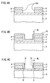
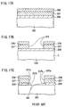
- Figs. 17A through 17C and Figs. 18A through 18C illustrate schematic partial cross sectional structures obtained during a conventional manufacturing process of a portion around the intrinsic base 211 in the conventional vertical bipolar transistor shown in Figure 16.
- the collector epitaxial silicon layer 203 of the silicon basic body 200 is fabricated by using any appropriate method.
- the silicon oxide film 206, the p+type base electrode polysilicon film 207 and the silicon nitride film 208 are formed in this order.
- the polysilicon film 207 is patterned in areas not shown in the drawing by using, for example, photolithography and etching, before forming the silicon nitride film 208.
- an opening 301 is formed so as to penetrate a silicon nitride film 208 and a polysilicon film 207 by using, for example, photolithography and etching.
- an opening 302 is formed so as to penetrate a silicon oxide film 206 by using etching and the like.
- a p+ type single crystal silicon intrinsic base 211 is formed on the exposed portion of the collector epitaxial silicon layer 203 by means of a vapor phase epitaxial growth method, and at the same time a p+ type polysilicon film 212 is formed on the exposed portion 207a of the side surface and the exposed portion 207b of the lower surface of the base electrode polysilicon film 207. Since the collector epitaxial silicon layer 203 is a single crystal, the p+ type single crystal intrinsic base 211 formed on the collector layer 203 becomes a single crystal in the same way.
- the base electrode polysilicon film 207 is polycrystalline, the p+ type silicon film 212 formed on the exposed portion 207a of the side surface and the exposed portion 207b of the lower surface of the base electrode polysilicon film 207 becomes polycrystalline in the same way.
- the silicon oxide film spacer 213 is formed so as to cover the inner side wall of the opening 301, by etching back of the silicon oxide film by means of an anisotropic etching process.
- an n++ type emitter electrode polysilicon 216 is formed by depositing and patterning n++ polysilicon.
- n type impurity inside the n++ type emitter electrode polysilicon 216 is diffused into the surface area of the p+ type single crystal silicon intrinsic base 211 and an n++ type single crystal silicon emitter region 215 is formed. Thereby, a structure shown in Fig. 18C is obtained.
- the inventor considered on the base electrode polysilicon film 207 in detail. It has been reported that in case that nondoped or additive-free (namely, no impurity added) polysilicon is deposited at a temperature within a range from approximately 600 to 650 degrees Celsius, the grain size in the deposited polysilicon film is 0.03 to 0.3 ⁇ m and its orientation is a ⁇ 110 ⁇ . And when impurities are doped into the polysilicon film and, thereafter, a heat treatment for activating impurity atoms is performed, the grain size in the polysilicon film becomes 0.5 to 3 ⁇ m, namely, larger than the grain size immediately after deposition.
- direction of crystal lattice planes of exposed surface of each grain at the exposed portion 207a of the side surface of the polysilicon film 207 formed by almost vertically dry-etching the polysilicon film is a direction perpendicular to the ⁇ 110 ⁇ plane, but if higher order direction of lattice planes is also considered, countless directions may exist.
- an emitter region needs to become various sizes depending on the circuit structure.
- the longitudinal dimension of an emitter can become about 2 ⁇ m to 16 ⁇ m or 32 ⁇ m.
- an effective emitter area corresponds to a designed emitter area and a collector current increases or decreases in proportion to the effective emitter area.
- approximately the same collector currents flow through transistors having the same size.
- the longitudinal dimension of an emitter is small, a not so many number of crystal grains are exposed at the exposed portion 207a of the side surface of the polysilicon film 207.
- the direction of crystal lattice planes of the exposed surface of each crystal grain at the inner surface of the opening 301, that is, at the exposed portion 207a of the side surface of the polysilicon film 207 is the direction perpendicular to the ⁇ 110 ⁇ plane.
- higher order direction of lattice planes there are various directions depending on the grains even in the same opening 301, and, also, when compared the directions with respect to a plurality of openings 301 with one another, there are different directions depending upon the respective openings 301.
- Epitaxial growth rate of silicon varies considerably depending upon the direction of crystal lattice planes of a surface which becomes a seed of growth.
- the directions for every openings 301 with one another especially in case of small openings 301, the directions of crystal lattice planes of grains exposed at the inner surface of the openings 301 are different from one another.
- the thickness of the polysilicon film 212 epitaxially growing from the exposed portion 207a of the side surface and the exposed portion 207b of the lower surface of the base electrode polysilicon film 207 that is, the projection size W A considerably varies among openings 301.
- an intrinsic base is formed by a selective epitaxial growth method in a condition where the side surface portion 207a of the base electrode polysilicon film 207 is completely exposed.
- the thickness W A of the polysilicon film 212 grown on the side surface portion 207a of the base electrode polysilicon film 207 varies among opening 301.
- a silicon oxide film is formed so as to cover the whole area of the substrate and then the silicon oxide film is etched back by means of an anisotropic etching process to form a silicon oxide film spacer 213 covering the inner side wall portion of the opening 301.
- the thickness W A of the polysilicon film 212 varies among openings 301 and it is difficult to make it constant.
- the size WB of the opening 304 defined by the silicon oxide film spacer 213 covering the inner side wall of the opening 301 varies among openings 301. That is to say, the exposed surface of a p+ type single crystal silicon intrinsic base 211 exposed by the opening 304 defined by the silicon oxide film spacer 213 varies in area.
- n++ type emitter electrode polysilicon 216 formed by depositing and patterning n++ polysilicon, an n type impurity inside the n++ type emitter electrode polysilicon 216 is diffused into the surface area of the p+ type single crystal silicon intrinsic base 211 and an n++ type single crystal silicon emitter region 215 is formed. Therefore, the n++ type single crystal silicon emitter region 215 also varies in size depending upon each opening 301. Namely, an emitter varies in area. As a result, it has become apparent that electric characteristics of a vertical bipolar transistor having such a constitution as described above and shown in Fig. 16 vary, and the above-mentioned ⁇ VB becomes large.
- the inventor of the present invention have invented a manufacturing method and a structure of a transistor which is not influenced by the variation in the thickness of a polysilicon film epitaxially grown selectively from the side surface of a base electrode polysilicon film and which varies little in electric characteristics.
- an insulating side wall spacer is formed on a part of the side surface of a first semiconductor layer corresponding to a base electrode polysilicon film, the thickness of the insulating side wall spacer W D is made thicker than the maximum thickness W F within a range of variation of the thickness W E of a polycrystalline film grown on the side surface of the base electrode polysilicon film, that is, the maximum thickness of the polycrystalline film (namely, W D > W F ).
- the size of the opening W G in an intrinsic base on which an emitter electrode polysilicon is deposited is not regulated by the size of the projecting portion of the polycrystalline film projecting inward the opening formed in the base electrode polysilicon film but is regulated by the side wall formed on a part of the side surface of the base electrode polysilicon film.
- a first semiconductor layer corresponding to a base electrode polysilicon is single-crystallized.
- an intrinsic base and a base electrode polysilicon film can be connected to each other only by the growth of a single crystal, by making the thickness W H of an intrinsic base single crystal film formed by means of a selective crystal growth method thicker than the spacing W I between the upper surface of a collector epitaxial silicon layer and the lower surface of the base electrode polysilicon film (W H > W I ). Therefore, it is possible to avoid such a problem that an intrinsic base is not connected to a base electrode polysilicon film as the problem in case of a vertical bipolar transistor disclosed in Japanese Patent No.2,551,353.
- Embodiments of the present invention are described with reference to the accompanying drawings in the following. First, an npn type bipolar transistor to which the present invention has been applied is described, but the present invention can be also applied to a pnp type bipolar transistor. Also, as described later as another embodiment, the present invention can be also applied to a field effect transistor such as a JFET, an MOSFET and the like.
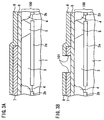
- Figure 1 is a vertical cross sectional view of a semiconductor device of a first embodiment of the present invention.
- a p- type silicon substrate 1 is prepared which has a surface of (100) plane and has an electrical resistivity from 10 to 20 ⁇ cm.
- Two kinds of buried layers are formed in an area of a few micrometers in thickness from the surface of a p- type silicon substrate 1.
- the two kinds of buried layers are an n+ type buried layer 2a and a channel stopper p+ type buried layer 2b, which exist separately from each other.
- An n- type epitaxial silicon layer 3 for a collector is formed on the surfaces of these buried layers 2a and 2b and on the surface of an area of the silicon substrate 1 where these buried layers 2a and 2b do not exist.
- the thickness of an effective epitaxial silicon layer for a collector is defined as the thickness of a region where the concentration of an n type impurity is 5x10 16 cm -3 or less, the thickness of the epitaxial silicon layer for a collector was about 0.60 ⁇ m (micrometer).
- a silicon oxide film 4 is formed by a LOCOS (LOCal Oxidation of Silicon) method.
- the silicon oxide film 4 is formed by converting an epitaxial silicon layer for a collector into a silicon oxide layer to the depth reaching the p+ type buried layer 2b.
- an n+ type collector lead-out region 5 connected to the n+ type buried layer 2a is formed in a part of the n- type epitaxial layer for a collector by doping impurities into it in a high concentration.
- the portions described so far are collectively called a silicon basic body 100, and this silicon basic body 100 is considered also as a substrate. Because of the existence of the n- type epitaxial silicon layer 3, the silicon basic body 100 can be considered as an n- type substrate.
- a silicon oxide film 6 is formed on the basic body 100 and a p+ type polysilicon film 7 for a base electrode is selectively formed on the silicon oxide film 6.
- An epitaxial silicon layer 3 for a collector is partially exposed by a first opening 101 formed in the p+ type base electrode polysilicon film 7 and a second opening 102 formed in the silicon oxide film 6.
- the width of the first opening 101 is smaller than the width of the second opening 102.
- a side surface portion of the base electrode polysilicon film 7 corresponding the inner wall of the first opening 101 projects horizontally from the side surface portion of the silicon oxide film 6 corresponding to the inner wall of the second opening 102.
- the base electrode polysilicon film 7 is covered with a silicon nitride film 8.
- a silicon nitride film 8 On the inner wall of the first opening 101, there is an insulating side wall spacer formed by depositing a silicon oxide film 9 and a silicon nitride film 10 in this order.
- a p+ type single crystal silicon intrinsic base 11 exists on the collector epitaxial silicon layer 3 inside the second opening 102.
- a p+ type polysilicon film 12 is formed on the lower part of the side surface portion of the base electrode polysilicon film 7 (namely, on a part not covered with the side wall of the silicon oxide film 9).
- the p+ type polysilicon film 12 connects the base electrode polysilicon film 7 and the p+ type single crystal silicon intrinsic base 11 to each other.
- In the middle and surface area in the intrinsic base 11 there is an n++ type single crystal silicon emitter region 15.
- a silicon oxide film 13 is also formed as the side wall spacer of the opening 101.
- an n type silicon collector region 14 doped with impurities in a higher concentration than the concentration of impurities in the original collector epitaxial silicon layer 3.
- an n++ type single crystal silicon emitter region 15 of a single crystal silicon there is an n++ type emitter electrode polysilicon 16.
- Contact holes 103a, 103b and 103c which penetrate the silicon oxide film 17 and, depending upon places, penetrate also the silicon nitride film 8 and the silicon oxide film 6 are formed. Also, a metal film of aluminum-based alloy and the like is formed so as to fill these contact holes 103a, 103b and 103c and is patterned to form an emitter electrode 18a, a base electrode 18b and a collector electrode 18c. These emitter electrode 18a, base electrode 18b and collector electrode 18c of aluminum-based alloy are respectively in contact with the emitter electrode polysilicon 16, the base electrode polysilicon layer 7 and the collector lead-out region 5.
- Figure 2A is a vertical cross sectional view of the basic body 100.
- a p- type silicon substrate 1 which has a surface of (100) plane and has a resistivity of about 10 to 20 ⁇ cm is prepared.
- An n+ type buried layer 2a and a p+ type buried layer 2b are formed in areas near the surface of the silicon substrate 1.
- a method for forming them is as follows.
- a silicon oxide film (not illustrated) is formed on the silicon substrate 1 by means of an ordinary CVD method or a thermal oxidation method.
- the thickness of the silicon oxide film is several hundreds nm (300 to 700 nm is preferable, and the following description will be done by taking 500 nm as an example).
- a patterned photoresist film is formed on the silicon oxide film by means of an ordinary photolithography method.
- the silicon oxide film which is formed on the silicon substrate 1 and which has a thickness of 500 nm is selectively removed by an ordinary wet etching method by using a hydrogen fluoride (HF) -based solution and by using this patterned photoresist as a mask material.
- HF hydrogen fluoride
- the photoresist is removed by means of an organic solution and then the surface of the silicon substrate inside an opening of the silicon oxide film is oxidized to a depth of 20 to 50 nm for the purpose of alignment in the photolithography process, and after this, arsenic is selectively introduced into a region of the silicon substrate having a thin silicon oxide film by ion implantation of arsenic.
- the acceleration energy of ion implantation needs to be so low as not to penetrate the silicon oxide film which becomes a mask material.
- a condition is suitable in that the concentration of impurities in the buried layer reaches the level of 1x10 19 cm -3 , and an acceleration energy of 70 keV and a dose of 5x10 15 cm -2 were adopted (as the implantation condition, for example, an acceleration energy of 50 to 120 keV and a dose of 1x10 15 to 2x10 16 cm -2 are suitable).
- the substrate is heat treated at a temperature of 1,000 to 1,150 degrees Celsius for the purpose of recovering damage caused by the ion implantation, and activation and driving-in of arsenic (here, a heat treatment was performed at 1,100 degrees Celsius for 2 hours in an atmosphere of nitrogen). In such a way an n+ type buried layer 2a is formed.
- the silicon oxide film of 500 nm in thickness is all removed by an HF-based solution, and a silicon oxide film of, for example, 100 nm in thickness is formed on the substrate 1 by oxidation (as the thickness, 50 to 250 nm is suitable). Also, patterning of a photoresist, ion implantation of boron (under a condition of 50 keV in energy and 1x10 14 cm -2 in dose), removal of the photoresist, a heat treatment for activation (at 1,000 degrees Celsius for 1 hour in an atmosphere of nitrogen) and the like are performed, and thereby a channel stopper p+ type buried layer 2b is formed.
- n- type silicon epitaxial layer 3 is formed on whole area of the substrate 1 by an ordinary method, for example, a CVD method.
- a temperature of 950 to 1050 degrees Celsius is suitable as a growth temperature, and SiH 4 or SiH 2 Cl 2 is used as a material gas and PH 3 is used as a doping gas.
- the n- type silicon epitaxial layer 3 contains impurities, that is, phosphorus, of 5x10 15 to 5x10 16 cm -3 in concentration and is 0.3 to 1.3 ⁇ m in thickness.
- the thickness of the portion of the epitaxial layer 3 where the impurity concentration is equal to or less than 5x10 16 cm -3 was about 0.6 ⁇ m.
- an n- type silicon epitaxial layer 3 is formed on the buried layers 2a and 2b and on the area of the silicon substrate 1 where these buried layers 2a and 2b do not exist.
- a LOCOS oxide film 4 for element isolation is formed.
- a method of forming it is as follows. First, on the surface of the epitaxial layer 3 a thermal oxide film of 20 to 50 nm in thickness (not illustrated) is formed and then a silicon nitride film of 70 to 150 nm in thickness (not illustrated) is formed on the thermal oxide film.
- photoresist (not illustrated) is deposited and the photoresist is patterned by photolithography.
- the silicon nitride film and the thermal oxide film are selectively removed by a dry etching process using the patterned photoresist as a mask.
- the silicon epitaxial layer 3 is also etched and a groove or trench is formed in the surface of the silicon epitaxial layer 3.
- the depth of the groove is suitably about half the thickness of an oxide film formed by a LOCOS method.
- the work piece is oxidized in a condition where an element area is protected by the silicon nitride film, and thereby a silicon oxide film for element isolation, namely, a LOCOS oxide film 4 is formed.
- the LOCOS oxide film has suitably a thickness reaching the buried layer 2b for a channel stopper, for example, a thickness of 300 to 1,300 nm. In this case the thickness was about 600 nm.
- the silicon nitride film is removed by a heated phosphoric acid.
- an n+ type collector lead-out region 5 is formed in order to reduce a collector resistance.
- a method for doing this is to dope phosphorus into this region by means of a diffusion or ion implantation method. That is to say, a photoresist film which is opened only in the collector lead-out region is formed by photolithography and phosphorus is ion-implanted at a condition of 100keV in acceleration energy and 5x10 15 cm -2 in dose via the opening of the photoresist film.
- the whole work piece is heat treated at 1,000 degrees Celsius for 30 minutes in an atmosphere of nitrogen, in order to activate the implanted phosphorus and recover damage caused by the ion implantation.
- a silicon basic body 100 shown in Figure 2B is formed. It should be noted that the silicon basic body 100 can be manufactured by using any various method other than the method mentioned above. Also, it is possible to consider the silicon basic body as a substrate. Further, because of the existence of the n- type epitaxial silicon layer 3, it is possible to consider the silicon basic body 100 as an n- type substrate.
- the surface of this silicon basic body 100 is covered with a silicon oxide film 6.
- the thickness of the silicon oxide film 6 may be approximately the same degree as the thickness of an intrinsic base. However, it is preferable that the thickness of the film is somewhat thinner than the thickness of the intrinsic base, and in this case it was 50 nm.
- a polysilicon film 7a is deposited on the silicon oxide film 6.
- the polysilicon film is suitably 150 to 350 nm in thickness, and in this case it was 250 nm in thickness.
- Boron ion is implanted into this polysilicon film 7a.
- the energy of ion implantation needs to be so low that the boron ion does not penetrate through the polysilicon film 7a, and the dose of impurities needs to be so high in concentration that the concentration of impurities becomes about 1x10 20 cm -3 .
- the implantation energy was 10 keV and the dose was 1x10 16 cm -2 .
- photoresist not shown in the drawing is deposited on the polysilicon film 7a and is patterned. Then, the polysilicon film 7a is selectively removed by dry etching by using the patterned photoresist as a mask. In such a way, as shown in Figure 3A, a p+ type base electrode polysilicon film 7 comprising the patterned polysilicon film 7a is formed.
- a silicon nitride film 8 is formed on all over the surface including the base electrode polysilicon film 7 and the silicon nitride film 8 and the polysilicon film 7 are patterned for forming an opening 101 by means of photolithography and the like.
- the method of doing this is as follows. First, a silicon nitride film 8 is deposited by an LPCVD (low pressure chemical vapor deposition) method to approximately 300 nm in thickness on the silicon oxide film 6 and the polysilicon film 7 (the silicon nitride film is suitably 100 to 500 nm in thickness).
- LPCVD low pressure chemical vapor deposition
- an opening is formed in a portion of the photoresist where an intrinsic base is formed in the future by means of an ordinary photolithography.
- the silicon nitride film 8 and the base electrode polysilicon film 7 are successively removed selectively by an anisotropic dry etching process using this photoresist as a mask.
- an opening formed in the base electrode polysilicon film 7 is set as a first opening 101.
- the photoresist used as a mask is removed and the structure of Figure 3B is completed.
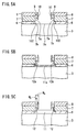
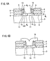
- Figures 4A to 4C, 5A to 5C, 6A and 6B are partial enlarged views of an area around the opening 101, and Figure 4A and Figure 3B show the structures at the same process step.
- a silicon oxide film 9 is formed all over the surface of a wafer by means of an LPCVD method.
- the thickness W C of this silicon oxide film 9 is not less than the maximum thickness W F within a range of dispersion of the thickness W E of a polycrystalline layer 12 grown on the side surface of the base electrode polysilicon film 7 at the same time as when epitaxial-growing an intrinsic base 11 mentioned later.
- the thickness W C of the silicon oxide film 9 was about 50 nm.
- a silicon nitride film 10 is formed by means of the LPCVD method on the silicon oxide film 9.
- the silicon nitride film 10 was 80 nm in thickness.
- the silicon nitride film 10 and the silicon oxide film 9 are etched back by an anisotropic dry etching process, and the silicon oxide film 6 is partially exposed.
- a side wall spacer comprising the remaining silicon nitride film 10 and the silicon oxide film 9 is left on the inner wall of the opening 101.
- the thickness W D of the side wall spacer composed of the silicon nitride film 10 and the silicon oxide film 9 left on the side surface of the opening 101 is naturally thicker than the thickness of the silicon oxide film 9 of approximately 50 nm in thickness.
- the thickness W D of the side wall spacer is larger than the maximum thickness W F within a range of dispersion of the thickness W E of the polycrystalline layer 12 grown on the side surface of the base electrode polysilicon film 7 at the same time as when epitaxial-growing an intrinsic base 11 described later.
- the silicon oxide film 6 is etched by an HF-based solution and the collector epitaxial silicon layer 3 is partially exposed.
- the silicon oxide film 9 is also partially etched and the lower portion 7a of the side surface of the base electrode polysilicon film 7 is exposed. Since the etching of the silicon oxide film 6 also propagates laterally, the end surface of the silicon oxide film 6 retreats laterally from the end surface of the base electrode polysilicon film 7 (namely, from the side wall of the first opening 101). The end surface of this silicon oxide film 6 makes the side wall of the above-mentioned second opening 102. Thereby, a portion 7b of the lower surface in the proximity of the end surface of the base electrode polysilicon film 7 is also exposed.
- Figure 5B is a vertical cross sectional view of the work piece in a middle stage of forming an intrinsic base by means of a selective crystal growth method.
- An LPCVD method, a gas source MBE method and the like can be used as a growth method, but here a UHV (Ultra High Vacuum)/CVD method is described as an example.
- a substrate temperature of 605 degrees Celsius is used, an Si 2 H 6 having a flow rate of 3 sccm is used as material gas, and a small amount of B 2 H 6 is used as a doping gas.
- silicon doped with boron in a low concentration is selectively grown.
- a p type polysilicon film 12a is grown from the exposed portion 7a of the side surface and the exposed portion 7b of the lower surface of the base electrode polysilicon film 7.
- a base region 11a composed of a p type single crystal silicon is grown on an exposed portion 3a of the silicon collector layer 3.
- Figure 5C is a cross sectional view of the work piece in a stage where an intrinsic base 11 and a p+ type polysilicon film 12 connecting the intrinsic base 11 to the base electrode polysilicon film 7 have been formed by means of a selective crystal growth method.
- the p type polysilicon film 12 grown from the exposed portion 7a of the side surface and the exposed portion 7b of the lower surface of the base electrode polysilicon film 7 and the base region 11 composed of a p type single crystal silicon grown from the exposed portion 3a of the silicon collector layer 3 are connected to each other as a result of the growth of them.
- the concentration of boron as impurities in the polysilicon film 12 and the base region 11 is, for example, 5x10 18 cm -3 , and the film thickness of the intrinsic base 11 is 60 nm for example.
- the thickness W E of the p+ type polysilicon film 12 disperses.
- the average film thickness of the p+ type polysilicon films 12 is, for example, 40 nm and the maximum thickness W F within a range of dispersion is 50 nm.
- a silicon oxide film of 100 nm in thickness is formed on whole surface of the substrate including the p+ type single crystal silicon intrinsic base region 11 by means of an LPCVD method.
- the silicon oxide film is etched back by means of an anisotropic dry etching process.
- a silicon oxide film spacer 13 of approximately 100 nm in thickness is formed as the side wall inside the opening 101.
- an n type collector region 14 is formed in the collector epitaxial silicon layer 3 directly under the intrinsic base 11 by ion implantation of phosphorus.
- the condition of phosphorus ion implantation was 200 keV in acceleration energy and 4x10 12 cm -2 in dose as an example.
- a phosphorus-doped polysilicon film of about 250 nm in thickness is deposited on whole surface of the substrate by means of the LPCVD method.
- the polysilicon film is patterned by the photolithography and the anisotropic dry etching.
- an n+ type emitter electrode polysilicon film 16 is formed.
- An n++ type single crystal silicon emitter region 15 is formed by diffusion of impurities contained in the n+ type emitter electrode polysilicon film 16 into the area around the surface of the intrinsic base 11.
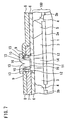
- Figure 7 is a vertical cross sectional view showing a whole semiconductor device at the stage of Figure 6B.
- openings 103a, 103b and 103c reaching respectively the emitter electrode polysilicon film 16, the base electrode polysilicon film 7 and the collector lead-out region 5 are formed by means of the photolithography and the anisotropic dry etching process as openings for forming metal electrodes.
- aluminum alloy film is formed on whole surface of the substrate by sputtering and patterned by photolithography and dry etching. Thereby, an emitter aluminum alloy electrode 18a, a base aluminum alloy electrode 18b and a collector aluminum alloy electrode 18c are formed. In this way, a semiconductor device of Figure 1 is fabricated.
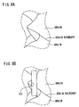
- Figure 8A is an enlarged partial plan view which schematically illustrates grains and grain boundaries at the upper surface of a base electrode polysilicon film 7 before forming the opening 101.
- Figure 8B is an enlarged partial plan view showing the relation in position of the opening 101 to the grains and grain boundaries flatly shown in Figure 8A.
- the opening 101 is disposed so that its inner wall surface cuts across some grain boundaries.
- Direction of crystal lattice planes can differ in different grains. Therefore, direction of crystal lattice planes at the inner wall is not uniform.
- the thickness W D of the p type polysilicon film 12 grown from the exposed portion 7a of the side surface and the exposed portion 7b of the lower surface of the base electrode polysilicon 7 is influenced by the directions of crystal lattice planes of the grains appearing at the exposed portions 7a and 7b, and disperses depending on each opening 101. In case that the openings 101 are small, dispersion of thickness W D of the p type polysilicon film 12 becomes considerably large.
- the thickness W D of the side wall spacer composed of the silicon nitride film 10 and the silicon oxide film 9 being left on the side wall of the opening 101 can be made thicker than the maximum thickness W F within a range of variation of the thickness W E of the p type polysilicon film 12 grown from the exposed portion 7a of the side surface and the exposed portion 7b of the lower surface of the base electrode polysilicon 7 exposed in the opening 101.
- the size W G of an opening 104 defined by the silicon oxide film 13 is not influenced by the dispersion of the thickness W E of the polysilicon film 12.
- the area in which the emitter electrode polysilicon film 16 and the p+ type single crystal silicon intrinsic base region 11 are in contact with each other, that is, the emitter size, can be made almost as designed without being influenced by the variation in thickness W E of the p type polysilicon film 12.
- a differential transistor pair is formed by short-circuiting with each other the emitters of transistors which are adjacent to each other. It is assumed that voltages to be applied to the bases so that the collector currents of the respective transistors of this differential transistor pair are equal to each other are VB1 and VB2, respectively. The difference between these voltages, namely, the absolute value of (VB1 - VB2) is defined as ⁇ VB.
- this ⁇ VB is as small as possible. The reason is that in case of combining some stages of differential transistor pairs, necessary input potential varies due to occurrence of changeover of the differential transistor pairs.
- Figures 9A, 9B and 9C are vertical enlarged cross sectional views each showing a partial structure obtained during a process for manufacturing the semiconductor device of the second embodiment.
- Figures 9A, 9B and 9C show structures corresponding to those of Figures 5A, 5C and 6B in the first embodiment.
- the opening 102 formed by lateral retreat of the end surface of the silicon oxide film 6 and the side wall spacer composed of the silicon nitride film 10 and the silicon oxide film 9 are formed, and process steps up to these are the same as those described with reference to Figure 5A in the first embodiment.
- a p type polycrystalline SiGe film 21, grown from the exposed portion 7a of the side surface and the exposed portion 7b of the lower surface of the base electrode polysilicon film 7, is formed.
- the p type polycrystalline SiGe film 21 was formed by means of a UHV/CVD method.
- An example of growth conditions is a substrate temperature of 605 degrees Celsius, an Si 2 H 6 flow rate of 3 sccm and a GeH 4 flow rate of 2 sccm.
- a base region 22 composed of a p type single crystal SiGe alloy is formed on an exposed portion 3a of the silicon collector layer 3. These polycrystalline SiGe alloy film 21 and SiGe alloy base region 22 are in contact with each other.
- the intrinsic base layer is composed of two layers. First, a nondoped SiGe layer is grown on the exposed portion 3a of the silicon collector 3 inside the opening 101 by means of a selective epitaxial growth method. The concentration of Ge was about 10 percent. The thickness of the grown film is about 25 nm. It is a matter of course that it is possible to make thicker the film thickness within a range where no defect occurs by means of a heat treatment of a later process.
- a nondoped polycrystalline SiGe film is grown also from the exposed portion 7a of the side surface and the exposed portion 7b of the lower surface of the p+ type polysilicon film 7 at the same time.
- a heat treatment is performed in order to dope boron in a high concentration into the nondoped polycrystalline SiGe film.
- boron diffuses from the polysilicon film 7 into the nondoped polycrystalline SiGe film, and the nondoped polycrystalline SiGe becomes a p+ type polycrystalline SiGe film.
- a p+ type SiGe graded layer having a graded Ge profile is formed on the nondoped SiGe film.
- An example of a Ge profile of the p+ type SiGe graded layer, a concentration profile of boron as impurities and its film thickness is described.
- the thickness of the p+ type SiGe graded layer having a profile in which the concentration of Ge in SiGe decreases linearly from 10 percent to 0 percent as approaching to the surface is 40 nm.
- This layer is doped with boron of 5x10 18 cm -3 in concentration.
- Figure 9B is a cross sectional view of the work piece in a stage where a single crystal silicon film 23 and a polycrystalline silicon layer are formed by means of a selective crystal growth method thereafter. That is to say, a layer 23 of about 30 nm in thickness purely composed of Si without containing Ge exists on the intrinsic base 22.
- the intrinsic base 22 and the polycrystalline layer 21 each properly having two-layer structure are shown as having one-layer structure for convenience.
- a silicon oxide film spacer 13 which is a side wall spacer is formed by using deposition of a silicon oxide film and etching back and the like.
- a n type collector region 14 is formed by ion implantation and the like into the collector epitaxial layer 3 just under the intrinsic base 22.
- a polysilicon film doped with phosphorus is deposited and patterned by using photolithography, etching and the like, so that, as shown in Figure 9C, an n++ type emitter electrode polysilicon 16 is formed.
- an n++ type single crystal silicon emitter region 24 is formed in a single crystal silicon film 23 by using heat treatment and the like. Thereby, the structure shown in Figure 9C is completed.
- This structure corresponds to the structure shown in Figure 6B in the first embodiment. Processes after this are the same as the first embodiment, and an explanation thereof is omitted here.
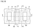
- Figure 10 is a schematic plan view of a semiconductor device of the third embodiment.
- Figure 11A is a schematic vertical cross sectional view of the semiconductor device taken along line B-B of Figure 10 and an FET current flows in the horizontal direction on the drawing sheet.
- Figure 11B is a schematic vertical cross sectional view of the semiconductor device taken along line C-C of Figure 10 and an FET current flows in the direction perpendicular to the drawing sheet.
- Figure 12 is a schematic vertical cross sectional view of the semiconductor device of the third embodiment of the present invention taken along line D-D of Figure 10 and an FET current flows in the direction perpendicular to the drawing sheet.
- a source electrode polysilicon film 32 and a drain electrode polysilicon film 33 are divided into two by the patterning of the gate. Since only the main surface of an n- type silicon substrate 31 inside the end of a LOCOS is exposed, a selective epitaxial growth is performed only on the element forming area.
- a silicon oxide film 4 for element isolation is formed in the main surface of the n- type silicon substrate 31 by a LOCOS method.
- the main surface of the n- type silicon substrate 31 surrounded by the silicon oxide film 4 is exposed, thereby a device or element forming area is defined and formed.
- a structure formed on the main surface of the n- type silicon substrate 31 in which the silicon oxide film 4 has been formed corresponds to a structure in which the right half is also formed symmetrically to the left half with respect to the center of the intrinsic base 11 in the structure formed on the surface of the silicon basic body 100 in Figure 1.
- the main surface of the silicon substrate 31 is covered with a silicon oxide film 6. It is suitable that the thickness of the silicon oxide film 6 is approximately the same as the thickness of a p type channel silicon film 34 described later.
- a polysilicon film is deposited and, for example, p type impurities such as boron are ion-implanted into the polysilicon film.
- photoresist is deposited on the polysilicon film and the photoresist is patterned, and then unnecessary polysilicon film is removed by dry etching process using this photoresist as a mask. Thereby, a source/drain electrode polysilicon film is formed which is to be formed into the source electrode polysilicon film 32 and the drain electrode polysilicon film 33 in the future but is not yet divided into them.
- a silicon nitride film 8 is formed and then a photoresist film is formed on the silicon nitride film 8. Next, an opening is formed in the photoresist film on the area in which a p type channel is to be formed in the future, by means of an ordinary photolithography. Following this, the silicon nitride film 8 and the source/drain electrode polysilicon film under this silicon nitride film 8 are successively and selectively removed by means of an anisotropic dry etching process using this photoresist as a mask.
- the opening formed in the silicon nitride film 8 and the source/drain electrode polysilicon film is set as a first opening 101 in a manner similar to the first embodiment. Also, the source/drain electrode polysilicon film is divided by the first opening 101 into the source electrode polysilicon 32 and the drain electrode polysilicon 33.
- a silicon oxide film 9 is formed all over the wafer in the same way as Figure 4B of the first embodiment and a silicon nitride film 10 is formed on the silicon oxide film 9.
- the silicon oxide film 6 is partially exposed by etching back the silicon nitride film 10 and the silicon oxide film 9 by means of an anisotropic dry etching process.
- the side wall of W D in thickness composed of the silicon nitride film 10 and the silicon oxide film 9 left as the result thereof is left on the side surface of the opening 101, in a manner similar to the first embodiment.
- the main surface of the silicon substrate 31 is exposed partially by etching the exposed silicon oxide film 6 by means of an HF-based solution.
- the silicon oxide film 9 is also etched and the lower portion of the side surface of each of the source electrode polysilicon film 32 and the drain electrode polysilicon film 33 is exposed.
- the end surface of the silicon oxide film 6 retreats laterally from the respective end surfaces (namely, inner walls of the opening 101) of the source electrode polysilicon film 32 and the drain electrode polysilicon film 33.
- the end surface of this silicon oxide film 6 corresponds to the second opening 102.
- a p+ type channel single crystal silicon film 34, and p type polysilicon films 35 and 36 connecting the p+ type channel single crystal silicon film 34 respectively to the side surfaces of the source electrode polysilicon film 32 and the drain electrode polysilicon film 33 are formed by means of a selective crystal growth method in the same manner as shown in Figures 5B and 5C of the first embodiment.
- a silicon oxide film is formed on the surface including the p type channel silicon film 34, by using an LPCVD method.
- an anisotropic dry etching process is performed to etch back the silicon oxide film and in the same manner as Figure 6A of the first embodiment, a silicon oxide film spacer 13 is formed as the side wall inside the opening 101.
- a phosphorus-doped polysilicon is deposited by means of an LPCVD method. Furthermore, this polysilicon film is patterned by photolithography and anisotropic dry etching. In this way, as shown in Figure 11A, an n++ type polysilicon film 37 is formed. At this time, an n++ type single crystal silicon region 38 is formed in the region in the proximity of the surface of the p type channel single crystal silicon film 34 which is in contact with the n++ type polysilicon film 37.
- openings for forming metal electrodes openings 139a, 139b and 139c reaching respectively the source electrode polysilicon film 32, the gate electrode polysilicon film 37 and the drain electrode polysilicon film 33 are formed by photolithography and anisotropic dry etching.
- an aluminum alloy film is formed by sputtering and is patterned by means of photolithography and dry etching. Thereby, a gate aluminum alloy electrode 39a, a source aluminum alloy electrode 39b and a drain aluminum alloy electrode 39c are formed, and thereby a semiconductor device of this embodiment is fabricated.
- this third embodiment it is possible to effectively suppress dispersion in size of the n++ type single crystal silicon region 38, similarly to the first embodiment in which dispersion in the size of the n++ type single crystal silicon emitter region 15 can be effectively suppressed. Therefore, it is possible to minimize dispersion or variation in electric characteristics of a junction FET.
- Figure 13 is a vertical cross sectional view of a semiconductor device of the fourth embodiment of the present invention
- Figures 14A, 14B and 15 are its vertical cross sectional views in a main process for manufacturing the semiconductor device of the fourth embodiment.
- Figure 13 and Figures 14A and 14B portions corresponding to the portions shown in Figure 1 are given the same reference numbers as those of Figure 1 and description of them is omitted.
- a method for forming a base electrode single crystal silicon film 51 which is used in place of the base electrode polysilicon film 7 of the first embodiment is described in the following.
- the fourth embodiment of the present invention is approximately the same as the first embodiment until the silicon oxide film 6 is formed on the silicon basic body 100 and an explanation thereof is omitted here.
- an opening 502 is formed in a portion of the silicon oxide film 6 through which a collector electrode is led out, by using photolithography, etching and the like. After this opening has been formed, an amorphous silicon film 50 is deposited on the silicon oxide film 6. Thereby, the structure shown in Figure 14A is completed.
- a solid epitaxial growth process is performed using as a core the surface portion of the silicon single crystal substrate 3 inside the opening 502.
- a laser annealing method for example is used as the solid epitaxial growth method in which the amorphous silicon film 50 is heated by a laser light.
- the amorphous silicon film 50 is heated by a laser light.
- a base electrode single crystal silicon film 51 and a collector electrode single crystal silicon film 52 are formed by patterning a silicon film 50 which is at least partially single-crystallized in such a way. Thereby, the structure of Figure 14B is completed.
- a silicon nitride film 8 is formed all over the wafer.
- a photoresist film not shown in the drawing is formed on the silicon nitride film 8 and patterned by using an exposure mask.
- the silicon nitride film 8 and the base electrode single crystal silicon film 51 are selectively removed by using the patterned photoresist film as an etching mask.
- an opening 501 is formed.
- This opening 501 corresponds to the opening 101 of the first embodiment.
- an exposure mask for patterning the photoresist film is previously designed, for example, as dimensions by which the structure having dimensions shown in Figure 13 can be formed, an opening 501 can be formed within about 5 ⁇ m from the opening 502.
- the opening 501 is contained sufficiently in the single-crystallized region.
- This opening 501 penetrates through the silicon nitride film 8 and the base electrode single crystal film 51.
- the side surface of the silicon film 51 exposed in the opening 501 is a single crystal surface.
- the side surface portion of the base electrode single crystal silicon film 51 exposed by the opening 501 is a single crystal. Therefore, the silicon film 53 grown at the exposed portions of the side surface and the lower surface of the base electrode single crystal silicon film 51 is also a single crystal, and thickness thereof becomes uniform and does not disperse.
- This silicon film 53 corresponds to the polysilicon film 12 of the first embodiment.
- the side wall spacer composed of the silicon nitride film 10 and the silicon oxide film 9 left on the side surface of the opening 501 can be omitted according to circumstances. Therefore, for example, in the conventional semiconductor device of Figure 16, in place of the polysilicon film 207, it is possible to use the single crystal silicon film 51 of this embodiment to obtain advantageous effect.
- the size of an opening for forming an emitter electrode polysilicon film on an intrinsic base or the size of an opening for forming a gate electrode polysilicon film on a channel layer is not influenced by the thickness of a polycrystalline film epitaxially growing from the side surface of the polysilicon film for the base electrode or source/drain electrode, but is defined by the side wall spacer formed on a portion of the side surface of the base electrode or source/drain electrode polysilicon film.
- emitter area or gate region area hardly disperses. Therefore, electric characteristics do not disperse but become stable.
- a silicon film for the base electrode or source/drain electrode is single-crystallized, a silicon film epitaxially grown from the side surface of the single-crystallized silicon film for a base electrode or source/drain electrode does not vary in thickness. Therefore, an opening for forming an emitter electrode polysilicon film on an intrinsic base or an opening for forming a gate electrode polysilicon film on a channel layer does not vary in size. Accordingly, variation in emitter area or gate region area is greatly suppressed, and electric characteristics of a semiconductor device do not disperse but become stable.
Landscapes
- Bipolar Transistors (AREA)
Applications Claiming Priority (2)
| Application Number | Priority Date | Filing Date | Title |
|---|---|---|---|
| JP468599 | 1999-01-11 | ||
| JP468599 | 1999-01-11 |
Publications (2)
| Publication Number | Publication Date |
|---|---|
| EP1020923A2 true EP1020923A2 (fr) | 2000-07-19 |
| EP1020923A3 EP1020923A3 (fr) | 2002-01-16 |
Family
ID=11590760
Family Applications (1)
| Application Number | Title | Priority Date | Filing Date |
|---|---|---|---|
| EP00100084A Withdrawn EP1020923A3 (fr) | 1999-01-11 | 2000-01-05 | Transistor bipolaire vertical et méthode pour sa fabrication |
Country Status (3)
| Country | Link |
|---|---|
| US (1) | US6680522B1 (fr) |
| EP (1) | EP1020923A3 (fr) |
| KR (1) | KR100321889B1 (fr) |
Cited By (2)
| Publication number | Priority date | Publication date | Assignee | Title |
|---|---|---|---|---|
| DE10038955A1 (de) * | 2000-08-09 | 2002-02-28 | Infineon Technologies Ag | Verfahren zur Herstellung eines Bipolartransistors |
| DE10160509A1 (de) * | 2001-11-30 | 2003-06-12 | Ihp Gmbh | Halbleitervorrichtung und Verfahren zu ihrer Herstellung |
Families Citing this family (8)
| Publication number | Priority date | Publication date | Assignee | Title |
|---|---|---|---|---|
| US6674102B2 (en) * | 2001-01-25 | 2004-01-06 | International Business Machines Corporation | Sti pull-down to control SiGe facet growth |
| KR100437494B1 (ko) * | 2002-03-25 | 2004-06-25 | 주식회사 케이이씨 | 트랜지스터 및 그 제조 방법 |
| US6861323B2 (en) * | 2003-02-21 | 2005-03-01 | Micrel, Inc. | Method for forming a SiGe heterojunction bipolar transistor having reduced base resistance |
| US20070278539A1 (en) * | 2006-06-02 | 2007-12-06 | Agere Systems Inc. | Junction field effect transistor and method for manufacture |
| US7893493B2 (en) * | 2006-07-10 | 2011-02-22 | International Business Machines Corproation | Stacking fault reduction in epitaxially grown silicon |
| US8946861B2 (en) * | 2013-06-11 | 2015-02-03 | International Business Machines Corporation | Bipolar device having a monocrystalline semiconductor intrinsic base to extrinsic base link-up region |
| US9722057B2 (en) * | 2015-06-23 | 2017-08-01 | Global Foundries Inc. | Bipolar junction transistors with a buried dielectric region in the active device region |
| DE102016216084B8 (de) * | 2016-08-26 | 2021-12-23 | Infineon Technologies Dresden Gmbh | Verfahren zum Herstellen eines Bipolartransistors |
Family Cites Families (18)
| Publication number | Priority date | Publication date | Assignee | Title |
|---|---|---|---|---|
| JPS63217663A (ja) | 1987-03-06 | 1988-09-09 | Fujitsu Ltd | 半導体装置の製造方法 |
| JPH0437143A (ja) | 1990-06-01 | 1992-02-07 | Fujitsu Ltd | 半導体装置 |
| JPH04105325A (ja) * | 1990-08-24 | 1992-04-07 | Hitachi Ltd | 半導体集積回路装置 |
| US5235206A (en) * | 1990-10-24 | 1993-08-10 | International Business Machines Corporation | Vertical bipolar transistor with recessed epitaxially grown intrinsic base region |
| US5391503A (en) | 1991-05-13 | 1995-02-21 | Sony Corporation | Method of forming a stacked semiconductor device wherein semiconductor layers and insulating films are sequentially stacked and forming openings through such films and etchings using one of the insulating films as a mask |
| JP3168622B2 (ja) | 1991-08-06 | 2001-05-21 | 日本電気株式会社 | 半導体装置及びその製造方法 |
| JP3149470B2 (ja) | 1991-09-12 | 2001-03-26 | 日本電気株式会社 | 半導体装置の製造方法 |
| JP2924417B2 (ja) | 1992-02-26 | 1999-07-26 | 日本電気株式会社 | 半導体装置 |
| JPH0817181B2 (ja) | 1992-11-13 | 1996-02-21 | 日本電気株式会社 | 半導体装置およびその製造方法 |
| JPH06168951A (ja) | 1992-12-01 | 1994-06-14 | Fujitsu Ltd | 半導体装置の製造方法 |
| JP3156436B2 (ja) | 1993-04-05 | 2001-04-16 | 日本電気株式会社 | ヘテロ接合バイポーラトランジスタ |
| JP2551353B2 (ja) | 1993-10-07 | 1996-11-06 | 日本電気株式会社 | 半導体装置及びその製造方法 |
| US5583059A (en) * | 1994-06-01 | 1996-12-10 | International Business Machines Corporation | Fabrication of vertical SiGe base HBT with lateral collector contact on thin SOI |
| JP2746225B2 (ja) | 1995-10-16 | 1998-05-06 | 日本電気株式会社 | 半導体装置及びその製造方法 |
| JP3555820B2 (ja) | 1997-01-17 | 2004-08-18 | 株式会社ルネサステクノロジ | バイポーラトランジスタおよびその製造方法 |
| US5773350A (en) | 1997-01-28 | 1998-06-30 | National Semiconductor Corporation | Method for forming a self-aligned bipolar junction transistor with silicide extrinsic base contacts and selective epitaxial grown intrinsic base |
| JPH10256269A (ja) | 1997-03-17 | 1998-09-25 | Sony Corp | 半導体装置の製造方法 |
| EP0878848A1 (fr) * | 1997-05-16 | 1998-11-18 | STMicroelectronics S.r.l. | Transistor bipolaire vertical de puissance à géométrie interdigitée et optimisation de la différence de potentiel base-émetteur |
-
1999
- 1999-12-29 US US09/474,504 patent/US6680522B1/en not_active Expired - Fee Related
-
2000
- 2000-01-05 EP EP00100084A patent/EP1020923A3/fr not_active Withdrawn
- 2000-01-10 KR KR1020000000861A patent/KR100321889B1/ko not_active Expired - Fee Related
Cited By (4)
| Publication number | Priority date | Publication date | Assignee | Title |
|---|---|---|---|---|
| DE10038955A1 (de) * | 2000-08-09 | 2002-02-28 | Infineon Technologies Ag | Verfahren zur Herstellung eines Bipolartransistors |
| DE10038955C2 (de) * | 2000-08-09 | 2002-07-11 | Infineon Technologies Ag | Verfahren zur Herstellung eines Bipolartransistors |
| DE10160509A1 (de) * | 2001-11-30 | 2003-06-12 | Ihp Gmbh | Halbleitervorrichtung und Verfahren zu ihrer Herstellung |
| US7323390B2 (en) | 2001-11-30 | 2008-01-29 | Ihp Gmbh - Innovations For High Performance Microelectronics/Institut Fur Innovative Mikroelektronik | Semiconductor device and method for production thereof |
Also Published As
| Publication number | Publication date |
|---|---|
| KR20000057734A (ko) | 2000-09-25 |
| US6680522B1 (en) | 2004-01-20 |
| EP1020923A3 (fr) | 2002-01-16 |
| KR100321889B1 (ko) | 2002-01-26 |
Similar Documents
| Publication | Publication Date | Title |
|---|---|---|
| US6713790B2 (en) | Semiconductor device and method for fabricating the same | |
| US5424572A (en) | Spacer formation in a semiconductor structure | |
| EP0375585B1 (fr) | Procédé pour fabriquer un dispositif du type BICMOS | |
| US6436781B2 (en) | High speed and low parasitic capacitance semiconductor device and method for fabricating the same | |
| KR100244812B1 (ko) | 반도체 장치 및 그 제조 방법 | |
| US6780725B2 (en) | Method for forming a semiconductor device including forming vertical npn and pnp transistors by exposing the epitaxial layer, forming a monocrystal layer and adjusting the impurity concentration in the epitaxial layer | |
| EP0701287A2 (fr) | Transistor bipolaire sans fuite de courant à travers la région de base mince et procédé de fabrication | |
| JPH088270A (ja) | 半導体装置およびその製造方法 | |
| US5194926A (en) | Semiconductor device having an inverse-T bipolar transistor | |
| KR100554465B1 (ko) | SOI 기판 위에 구현된 SiGe BiCMOS 소자 및그 제조 방법 | |
| JP3258123B2 (ja) | 半導体装置 | |
| US6461925B1 (en) | Method of manufacturing a heterojunction BiCMOS integrated circuit | |
| US6680522B1 (en) | Semiconductor device with reduced electrical variation | |
| JPH04330730A (ja) | 半導体装置及びその製造方法 | |
| US5430317A (en) | Semiconductor device | |
| JPH0340938B2 (fr) | ||
| US6103560A (en) | Process for manufacturing a semiconductor device | |
| US6080612A (en) | Method of forming an ultra-thin SOI electrostatic discharge protection device | |
| US6806159B2 (en) | Method for manufacturing a semiconductor device with sinker contact region | |
| JP2718257B2 (ja) | 集積回路における埋込み層容量の減少 | |
| JP3376208B2 (ja) | 半導体装置およびその製造方法 | |
| JP2697631B2 (ja) | 半導体装置の製造方法 | |
| KR100216510B1 (ko) | 트렌치를 이용한 바이폴라 트랜지스터의 컬렉터 형성방법 | |
| JP3303833B2 (ja) | 半導体装置及びその製造方法 | |
| JP3707978B2 (ja) | 半導体集積回路とその製造方法 |
Legal Events
| Date | Code | Title | Description |
|---|---|---|---|
| PUAI | Public reference made under article 153(3) epc to a published international application that has entered the european phase |
Free format text: ORIGINAL CODE: 0009012 |
|
| AK | Designated contracting states |
Kind code of ref document: A2 Designated state(s): DE FR GB IT NL |
|
| AX | Request for extension of the european patent |
Free format text: AL;LT;LV;MK;RO;SI |
|
| PUAL | Search report despatched |
Free format text: ORIGINAL CODE: 0009013 |
|
| AK | Designated contracting states |
Kind code of ref document: A3 Designated state(s): DE FR GB IT NL |
|
| AX | Request for extension of the european patent |
Free format text: AL;LT;LV;MK;RO;SI |
|
| 17P | Request for examination filed |
Effective date: 20011228 |
|
| AKX | Designation fees paid |
Free format text: DE FR GB IT NL |
|
| RAP1 | Party data changed (applicant data changed or rights of an application transferred) |
Owner name: NEC ELECTRONICS CORPORATION |
|
| STAA | Information on the status of an ep patent application or granted ep patent |
Free format text: STATUS: THE APPLICATION HAS BEEN WITHDRAWN |
|
| 18W | Application withdrawn |
Effective date: 20040908 |