EP1022784A2 - Cellule de SRAM et son procédé de fabrication - Google Patents
Cellule de SRAM et son procédé de fabrication Download PDFInfo
- Publication number
- EP1022784A2 EP1022784A2 EP00300390A EP00300390A EP1022784A2 EP 1022784 A2 EP1022784 A2 EP 1022784A2 EP 00300390 A EP00300390 A EP 00300390A EP 00300390 A EP00300390 A EP 00300390A EP 1022784 A2 EP1022784 A2 EP 1022784A2
- Authority
- EP
- European Patent Office
- Prior art keywords
- film
- transistors
- catalytic element
- load
- insulation film
- Prior art date
- Legal status (The legal status is an assumption and is not a legal conclusion. Google has not performed a legal analysis and makes no representation as to the accuracy of the status listed.)
- Withdrawn
Links
- 238000000034 method Methods 0.000 title claims abstract description 72
- 230000008569 process Effects 0.000 title claims description 12
- 238000004519 manufacturing process Methods 0.000 title description 5
- 230000003197 catalytic effect Effects 0.000 claims abstract description 54
- 229910021417 amorphous silicon Inorganic materials 0.000 claims abstract description 40
- 238000009413 insulation Methods 0.000 claims abstract description 33
- 239000007790 solid phase Substances 0.000 claims abstract description 29
- 230000004888 barrier function Effects 0.000 claims abstract description 20
- 238000009792 diffusion process Methods 0.000 claims abstract description 6
- 238000010438 heat treatment Methods 0.000 claims description 27
- 239000013078 crystal Substances 0.000 claims description 16
- 239000012298 atmosphere Substances 0.000 claims description 14
- 238000005247 gettering Methods 0.000 claims description 11
- 238000000059 patterning Methods 0.000 claims description 10
- 230000001590 oxidative effect Effects 0.000 claims description 9
- OAICVXFJPJFONN-UHFFFAOYSA-N Phosphorus Chemical compound [P] OAICVXFJPJFONN-UHFFFAOYSA-N 0.000 claims description 8
- 230000015572 biosynthetic process Effects 0.000 claims description 8
- 229910052698 phosphorus Inorganic materials 0.000 claims description 7
- 239000011574 phosphorus Substances 0.000 claims description 7
- 239000003870 refractory metal Substances 0.000 claims description 6
- 229910052736 halogen Inorganic materials 0.000 claims description 5
- 150000002367 halogens Chemical class 0.000 claims description 5
- XEEYBQQBJWHFJM-UHFFFAOYSA-N Iron Chemical group [Fe] XEEYBQQBJWHFJM-UHFFFAOYSA-N 0.000 claims description 4
- PXHVJJICTQNCMI-UHFFFAOYSA-N Nickel Chemical compound [Ni] PXHVJJICTQNCMI-UHFFFAOYSA-N 0.000 claims description 4
- KDLHZDBZIXYQEI-UHFFFAOYSA-N Palladium Chemical compound [Pd] KDLHZDBZIXYQEI-UHFFFAOYSA-N 0.000 claims description 4
- GWEVSGVZZGPLCZ-UHFFFAOYSA-N Titan oxide Chemical compound O=[Ti]=O GWEVSGVZZGPLCZ-UHFFFAOYSA-N 0.000 claims description 4
- PNEYBMLMFCGWSK-UHFFFAOYSA-N aluminium oxide Inorganic materials [O-2].[O-2].[O-2].[Al+3].[Al+3] PNEYBMLMFCGWSK-UHFFFAOYSA-N 0.000 claims description 4
- BASFCYQUMIYNBI-UHFFFAOYSA-N platinum Chemical compound [Pt] BASFCYQUMIYNBI-UHFFFAOYSA-N 0.000 claims description 4
- 229910052593 corundum Inorganic materials 0.000 claims description 3
- 239000011261 inert gas Substances 0.000 claims description 3
- 229910001845 yogo sapphire Inorganic materials 0.000 claims description 3
- RYGMFSIKBFXOCR-UHFFFAOYSA-N Copper Chemical compound [Cu] RYGMFSIKBFXOCR-UHFFFAOYSA-N 0.000 claims description 2
- KJTLSVCANCCWHF-UHFFFAOYSA-N Ruthenium Chemical compound [Ru] KJTLSVCANCCWHF-UHFFFAOYSA-N 0.000 claims description 2
- 229910020776 SixNy Inorganic materials 0.000 claims description 2
- 229910017052 cobalt Inorganic materials 0.000 claims description 2
- 239000010941 cobalt Substances 0.000 claims description 2
- GUTLYIVDDKVIGB-UHFFFAOYSA-N cobalt atom Chemical compound [Co] GUTLYIVDDKVIGB-UHFFFAOYSA-N 0.000 claims description 2
- 229910052802 copper Inorganic materials 0.000 claims description 2
- 239000010949 copper Substances 0.000 claims description 2
- PCHJSUWPFVWCPO-UHFFFAOYSA-N gold Chemical compound [Au] PCHJSUWPFVWCPO-UHFFFAOYSA-N 0.000 claims description 2
- 229910052737 gold Inorganic materials 0.000 claims description 2
- 239000010931 gold Substances 0.000 claims description 2
- 229910052741 iridium Inorganic materials 0.000 claims description 2
- GKOZUEZYRPOHIO-UHFFFAOYSA-N iridium atom Chemical compound [Ir] GKOZUEZYRPOHIO-UHFFFAOYSA-N 0.000 claims description 2
- 229910052742 iron Inorganic materials 0.000 claims description 2
- 229910052759 nickel Inorganic materials 0.000 claims description 2
- 229910052762 osmium Inorganic materials 0.000 claims description 2
- SYQBFIAQOQZEGI-UHFFFAOYSA-N osmium atom Chemical compound [Os] SYQBFIAQOQZEGI-UHFFFAOYSA-N 0.000 claims description 2
- 229910052763 palladium Inorganic materials 0.000 claims description 2
- 229910052697 platinum Inorganic materials 0.000 claims description 2
- 229910052703 rhodium Inorganic materials 0.000 claims description 2
- 239000010948 rhodium Substances 0.000 claims description 2
- MHOVAHRLVXNVSD-UHFFFAOYSA-N rhodium atom Chemical compound [Rh] MHOVAHRLVXNVSD-UHFFFAOYSA-N 0.000 claims description 2
- 229910052707 ruthenium Inorganic materials 0.000 claims description 2
- 239000007769 metal material Substances 0.000 claims 4
- 239000010408 film Substances 0.000 description 127
- 239000010410 layer Substances 0.000 description 43
- 239000000758 substrate Substances 0.000 description 16
- 238000010586 diagram Methods 0.000 description 8
- 239000000463 material Substances 0.000 description 8
- 238000005229 chemical vapour deposition Methods 0.000 description 7
- 230000010354 integration Effects 0.000 description 5
- 239000011248 coating agent Substances 0.000 description 4
- 238000000576 coating method Methods 0.000 description 4
- 238000002513 implantation Methods 0.000 description 4
- 150000002500 ions Chemical class 0.000 description 4
- 229910021332 silicide Inorganic materials 0.000 description 4
- FVBUAEGBCNSCDD-UHFFFAOYSA-N silicide(4-) Chemical compound [Si-4] FVBUAEGBCNSCDD-UHFFFAOYSA-N 0.000 description 4
- BLRPTPMANUNPDV-UHFFFAOYSA-N Silane Chemical compound [SiH4] BLRPTPMANUNPDV-UHFFFAOYSA-N 0.000 description 3
- 239000007789 gas Substances 0.000 description 3
- 230000006872 improvement Effects 0.000 description 3
- 238000004518 low pressure chemical vapour deposition Methods 0.000 description 3
- 229910000077 silane Inorganic materials 0.000 description 3
- 239000002904 solvent Substances 0.000 description 3
- 238000004544 sputter deposition Methods 0.000 description 3
- WFKWXMTUELFFGS-UHFFFAOYSA-N tungsten Chemical compound [W] WFKWXMTUELFFGS-UHFFFAOYSA-N 0.000 description 3
- 229910052721 tungsten Inorganic materials 0.000 description 3
- 239000010937 tungsten Substances 0.000 description 3
- IJGRMHOSHXDMSA-UHFFFAOYSA-N Atomic nitrogen Chemical compound N#N IJGRMHOSHXDMSA-UHFFFAOYSA-N 0.000 description 2
- 150000001875 compounds Chemical class 0.000 description 2
- 239000012535 impurity Substances 0.000 description 2
- 230000003071 parasitic effect Effects 0.000 description 2
- 238000000206 photolithography Methods 0.000 description 2
- 239000002994 raw material Substances 0.000 description 2
- 230000003068 static effect Effects 0.000 description 2
- 229910001218 Gallium arsenide Inorganic materials 0.000 description 1
- ATJFFYVFTNAWJD-UHFFFAOYSA-N Tin Chemical compound [Sn] ATJFFYVFTNAWJD-UHFFFAOYSA-N 0.000 description 1
- RTAQQCXQSZGOHL-UHFFFAOYSA-N Titanium Chemical compound [Ti] RTAQQCXQSZGOHL-UHFFFAOYSA-N 0.000 description 1
- 230000002411 adverse Effects 0.000 description 1
- 238000000137 annealing Methods 0.000 description 1
- QVGXLLKOCUKJST-UHFFFAOYSA-N atomic oxygen Chemical compound [O] QVGXLLKOCUKJST-UHFFFAOYSA-N 0.000 description 1
- 239000005380 borophosphosilicate glass Substances 0.000 description 1
- 230000015556 catabolic process Effects 0.000 description 1
- 238000002425 crystallisation Methods 0.000 description 1
- 230000008025 crystallization Effects 0.000 description 1
- 230000003247 decreasing effect Effects 0.000 description 1
- 238000006731 degradation reaction Methods 0.000 description 1
- 238000000151 deposition Methods 0.000 description 1
- PZPGRFITIJYNEJ-UHFFFAOYSA-N disilane Chemical compound [SiH3][SiH3] PZPGRFITIJYNEJ-UHFFFAOYSA-N 0.000 description 1
- 238000001035 drying Methods 0.000 description 1
- 230000000694 effects Effects 0.000 description 1
- 230000002708 enhancing effect Effects 0.000 description 1
- 238000005189 flocculation Methods 0.000 description 1
- 230000016615 flocculation Effects 0.000 description 1
- 239000007943 implant Substances 0.000 description 1
- 238000005468 ion implantation Methods 0.000 description 1
- 238000002955 isolation Methods 0.000 description 1
- 238000005224 laser annealing Methods 0.000 description 1
- 229910052751 metal Inorganic materials 0.000 description 1
- 239000002184 metal Substances 0.000 description 1
- 238000001465 metallisation Methods 0.000 description 1
- 238000012986 modification Methods 0.000 description 1
- 230000004048 modification Effects 0.000 description 1
- 229910021421 monocrystalline silicon Inorganic materials 0.000 description 1
- 150000004767 nitrides Chemical class 0.000 description 1
- 229910052757 nitrogen Inorganic materials 0.000 description 1
- 239000012299 nitrogen atmosphere Substances 0.000 description 1
- 230000003647 oxidation Effects 0.000 description 1
- 238000007254 oxidation reaction Methods 0.000 description 1
- 229910052760 oxygen Inorganic materials 0.000 description 1
- 239000001301 oxygen Substances 0.000 description 1
- 238000009832 plasma treatment Methods 0.000 description 1
- 238000005498 polishing Methods 0.000 description 1
- 239000004065 semiconductor Substances 0.000 description 1
- 238000001179 sorption measurement Methods 0.000 description 1
- 239000000126 substance Substances 0.000 description 1
- 239000002344 surface layer Substances 0.000 description 1
- 238000004381 surface treatment Methods 0.000 description 1
- 239000010409 thin film Substances 0.000 description 1
- 239000010936 titanium Substances 0.000 description 1
- 229910052719 titanium Inorganic materials 0.000 description 1
- 238000007740 vapor deposition Methods 0.000 description 1
Images




Classifications
-
- H—ELECTRICITY
- H10—SEMICONDUCTOR DEVICES; ELECTRIC SOLID-STATE DEVICES NOT OTHERWISE PROVIDED FOR
- H10B—ELECTRONIC MEMORY DEVICES
- H10B10/00—Static random access memory [SRAM] devices
-
- H—ELECTRICITY
- H10—SEMICONDUCTOR DEVICES; ELECTRIC SOLID-STATE DEVICES NOT OTHERWISE PROVIDED FOR
- H10B—ELECTRONIC MEMORY DEVICES
- H10B10/00—Static random access memory [SRAM] devices
- H10B10/12—Static random access memory [SRAM] devices comprising a MOSFET load element
- H10B10/125—Static random access memory [SRAM] devices comprising a MOSFET load element the MOSFET being a thin film transistor [TFT]
-
- H—ELECTRICITY
- H10—SEMICONDUCTOR DEVICES; ELECTRIC SOLID-STATE DEVICES NOT OTHERWISE PROVIDED FOR
- H10D—INORGANIC ELECTRIC SEMICONDUCTOR DEVICES
- H10D86/00—Integrated devices formed in or on insulating or conducting substrates, e.g. formed in silicon-on-insulator [SOI] substrates or on stainless steel or glass substrates
- H10D86/01—Manufacture or treatment
-
- Y—GENERAL TAGGING OF NEW TECHNOLOGICAL DEVELOPMENTS; GENERAL TAGGING OF CROSS-SECTIONAL TECHNOLOGIES SPANNING OVER SEVERAL SECTIONS OF THE IPC; TECHNICAL SUBJECTS COVERED BY FORMER USPC CROSS-REFERENCE ART COLLECTIONS [XRACs] AND DIGESTS
- Y10—TECHNICAL SUBJECTS COVERED BY FORMER USPC
- Y10S—TECHNICAL SUBJECTS COVERED BY FORMER USPC CROSS-REFERENCE ART COLLECTIONS [XRACs] AND DIGESTS
- Y10S257/00—Active solid-state devices, e.g. transistors, solid-state diodes
- Y10S257/903—FET configuration adapted for use as static memory cell
Definitions
- the present invention relates to an SRAM (static random access memory) cell and its fabrication process. More particularly, the invention relates to an SRAM cell constituted in such a manner that a load device is a thin film transistor and that the SRAM cell is of a three-dimensional structure and high in integration density and operates at a low voltage, and also to its fabrication process.
- SRAM static random access memory
- An SRAM cell is constituted from two inverters and two transfer transistors, wherein the two inverters are cross-connected and connected to bit lines by the two transfer transistors.
- the inverter is normally constituted from an NMOS driving transistor and a load device and applied with a supply voltage.
- Fig. 4A to Fig. 4C show typical SRAM cell structures.
- Fig. 4A to Fig. 4C three kinds of SRAM cells are shown; these SRAM cells differ in respect of the constitution and kind of a load device.
- a resistor composed of PolySi is used as a load device 101: in case of Fig. 4B, a transistor (called as a bulk transistor) formed on a substrate is used as the load device 101: and in case of Fig. 4C, a transistor (called as a stacked transistor) formed on a driving transistor 103 is used as the load device 101.
- FIG. 4C are called as a full CMOS type SRAM cell, particularly, the SRAM cell shown in Fig. 4B is called as a bulk full CMOS type SRAM cell.
- reference numerals 102 and 104 denote a transfer transistor and a bit line, respectively.
- the load devices 101 shown in Fig. 4A and C are desirably a resistor composed of PolySi or a stacked transistor. This is because the load device 101 can be formed on the driving transistor 103 formed on the substrate, so that the element area can be reduced.
- Fig. 5A is a diagram showing the sate of an SRAM cell.
- the robustness of the memory cell against unbalances, device mismatches and noise from power source and adjacent cells is characterized by the static noise margin: SNM.
- Fig. 5B shows a relation between the load device transconductance ⁇ p and SNM. In Fig. 5B, it is shown that the higher the ⁇ p, the larger the SNM; and accordingly, a higher margin can be obtained.
- the ⁇ p of the load device 101 is usually so high as about 3 ⁇ 10 -5 A/V 2 .
- the ⁇ p of the load device 101 shown in Fig. 4C is usually about 1 ⁇ 10 -7 A/V 2 , so that in case that the supply voltage is 1 V or lower, it is difficult to make the bulk full CMOS type SRAM cell sufficiently operate.
- the limit of the ON-state current of the load device 101 is 50 ⁇ A, but in case of the load device 101 shown in Fig. 4C, the limit of the ON-state current is 1 to 10 ⁇ A, and therefore, the cell can be used only at a high supply voltage.
- Fig. 6 shows I-V characteristics of the load devices shown in Fig. 4A and C.
- the cell in case that a PMOS formed on the driving transistor is used as the load device, the cell can drive a large current and operate at a lower voltage.
- a PolySi film is used in an active region. For this reason, in order to improve a mobility of this transistor, it is required to increase the grain size (grain diameter) of a crystal constituting the PolySi film.
- a method of increasing the grain size there is known a method according to which a PolySi film is solid phase grown epitaxially from an amorphous Si film, for example by subjecting the film to a heat treatment at about 600°C for about 30 hours or laser annealing.
- the quality of the PolySi film obtained by this method is not sufficient for use in an SRAM cell.
- the reason for this in case of this method, grain boundaries are scattered, so that the mobility is decreased, and at the same time, the characteristics of the SRAM cell are scattering. Further, since a long time and a high temperature are employed, the characteristics of the transistor formed on the substrate underneath the stacked transistor are deteriorated, this being also a problem.
- a portion of an insulation film 112 formed on a substrate 111 is bored to form an opening, and then, an amorphous Si film 113 is deposited and heat-treated, whereby a PolySi film is solid phase grown, with single crystal Si of the opening acting as a nucleus (Nobuhiko Oda, et al, Preprint of the 38th Physics-Related Engineers Association in Spring of 1991 , page 742 31p-X-12, "Solid Phase Growth of Si Using the U-LPCVD Method").
- arrows indicate a direction of the solid phase growth.
- photolithography must be performed at least twice at the step of forming the stepped portion and at the step of leaving the PolySi film existing near the stepped portion; and thus, there arises a problem that the manufacturing time is long.
- the catalytic element used reacts with Si to form a silicide, whereby there is fear that the transistors formed on the substrate are contaminated.
- a plug is used for connecting the transistors formed on the substrate to the stacked transistors each other. This plug needs to be formed directly beneath the stacked transistors in view of enhancing the integration density.
- the plug acts as a nucleus, as a result of which an undesirable crystal comes to be contained in the active region.
- an SRAM cell comprising, at least, two driving transistors and two transfer transistors, and two load transistors each comprised of a TFT and disposed on these transistors through a layer insulation film, the load transistors having an active region comprising an Si film having improved crystallizability of amorphous Si by the solid phase growth technique using a catalytic element, and a barrier layer for preventing the catalytic element from diffusion into the driving transistors and the transfer transistors which is disposed between the layer insulation film and the load transistors.
- a fabricating process of an SRAM cell which comprises covering two driving transistors and two transfer transistors with a layer insulation film; forming on the layer insulation film a barrier layer for preventing a catalytic element from diffusion into the driving transistors and the transfer transistors; forming an amorphous Si film on the barrier layer: forming an Si film having improved crystallizability of amorphous Si by the solid phase growth technique using the catalytic element; forming an active region by patterning the Si film to a desired shape; and stacking a gate insulation film and a gate electrode on the active region in this order to form a load transistor.
- two driving transistors and two transfer transistors are covered with a layer insulation film.
- the structures of the driving transistors and the transfer transistors are not particularly limited; any of known structures can be used.
- the driving transistors and the transfer transistors may be of either a P- or N-conductivity type.
- an element isolation region may be formed by the LOCOS method, the impurity implantation method or the like.
- the layer insulation film covering the driving transistors and the transfer transistors may comprise an Si oxide film, an Si nitride film, a PSG film or a BPSG film, or a film formed by stacking these films.
- a thickness of the layer insulation film varies depending on the material used, but usually is from 300 to 1,200 nm.
- the method of forming the layer insulation film is not particularly limited, but the CVD method, the thermal oxidation method, etc. are employable.
- the layer insulation film its surface is more desirably planarized in order to improve crystallizability of an amorphous Si film formed on the layer insulation film through a barrier layer.
- planarizing method any known method can be employed; for example, the CMP method (chemical mechanical polishing method) is enumerated.
- a barrier layer is formed for preventing a catalytic element from diffusion into the driving transistors and the transfer transistors.
- the material constituting this barrier layer include Al 2 O 3 , Si x N y , and TiO 2 .
- a thickness of the barrier layer usually is from 20 to 100 nm though it varies depending on the material used.
- the sputtering method and the CVD method are employable.
- a thickness of the amorphous Si film is usually from 30 to 60 nm though it varies depending on the material used.
- the method of forming the amorphous film is not particularly limited; any known method can be used. For example, the LPCVD method in which a silane-based compound such as silane (SiH 4 ) or disilane (Si 2 H 6 ) is used as a raw material gas is employable.
- an Si film having improved crystallizability of the amorphous Si film is formed.
- This Si film having improved crystallizability is composed of or composed mainly of PolySi. Particularly, it is preferred that this Si film is a PolySi film in view of more improvements in the mobility.
- This technique comprises a step of contacting the catalytic element with the amorphous Si film, a step of effecting crystal growth by heat treatment, and a step of gettering of the catalytic element by heat treatment.
- any catalytic element which can improve the crystallizability of Si can be used.
- Specific examples include iron, cobalt, nickel, ruthenium, rhodium, palladium, osmium, iridium, platinum, copper, and gold.
- the method of contacting the catalytic element with the amorphous Si film there can be used any of the method of applying a solution containing the catalytic element, the CVD method, the sputtering method, the vapor deposition method, the plasma treatment method and the gas adsorption method.
- the method of applying a solution is superior in respect of the adjustment of the amount of the solution supplied and the reproducibility.
- the solution containing a catalytic element for example a solution obtained by dissolving a compound of the catalytic element in a solvent can be used. Further, after the application, it is preferred that the solvent is removed by a means such as the spin-drying method.
- the step of solid phase growth of Si crystals proceeds in a desired direction of the amorphous Si film; for example, in case that the catalytic element is contacted with a surface of the amorphous Si film, the solid phase growth of Si crystals proceeds in the vertical direction of the film, while in case that the catalytic element is contacted with a side face of the amorphous Si film, the solid phase growth of Si crystals proceeds in the horizontal direction of the film.
- the temperature is 500 to 600°C, and the treating time is 1 to 6 hours.
- the temperature is lower than 500°C, or the time is shorter than 1 hour, the solid phase growth becomes insufficient, and therefore, this is not desirable.
- the temperature is higher than 600°C, or the time is longer than 6 hours, it is not desirable since a flocculation phenomenon takes place. Further, it is preferred that the heat treatment is carried out in an inert gas atmosphere.
- the catalytic element is adjusted so as to remain on the order of 10 18 cm -3 in the Si film having improved crystallizability.
- the catalytic element in the Si film is subjected to gettering.
- the heat treatment is carried out in, e.g., an oxidizing atmosphere containing a halogen element or in a non-oxidizing atmosphere after phosphorus is doped.
- an oxidizing atmosphere containing a halogen element for example, an oxygen atmosphere containing HCl, HF, HBr, Cl 2 , F 2 , Br 2 or CF 4 can be employed.
- the condition for the heat treatment is such a condition that an oxide film having a thickness of 20 nm is formed at 800°C.
- an atmosphere of an inert gas such as nitrogen is employable.
- condition for the heat treatment there is employed the condition that the heat treatment is carried out at a temperature on the order of from about 500 to 650°C. More specifically, in case that the temperature is 550°C, it is preferred that the heat treatment is carried out over several hours.
- the catalytic element is subjected to gettering in an oxide film formed on the Si film.
- the catalytic element is subjected to gettering in the region in which phosphorus is implanted.
- the technique disclosed in Japanese Unexamined Patent Publication No. HEI 9(1997)-107100, Japanese Unexamined Patent Publication No. HEI 9(1997)-312402, or Japanese Unexamined Patent Publication No. HEI 9(1997)-312404 can be utilized.
- the Si film into a desired shape, an active region is formed.
- the gettering of the catalytic element is effected in an oxidizing atmosphere containing a halogen element
- the oxide film formed on the Si film is removed, and then, the patterning of the Si film is carried out.
- the patterning is carried out so that the region in which phosphorus is doped may be included in the region to be removed.
- the patterning method there is no particular limitation; any of known methods can be used.
- a gate insulation film and a gate electrode are formed in this order on the active region, whereby each load transistor is formed.
- the gate insulation film and the gate electrode there is no particular limitation; they can be formed of known materials by known methods.
- the active region includes the source/drain regions, but these regions may be formed before the formation of the gate electrode, or may be formed, after the formation of the gate electrode, by the use of the gate electrode as a mask.
- the load transistors are be of the P-conductivity type in case that the driving transistors and the transfer transistorize are of the N-conductive type, and of the N-conductivity type in case that the driving transistors and the transfer transistors are of the P-conductive type, respectively.
- a throughhole may be formed through those regions of the driving transistors and the transfer transistors which are desired to be connected and through the active region, and then, the throughhole may be filled up with a wiring material to form a plug.
- the active region of the load transistor comes to be contacted, at its side walls, with the plug.
- PolySi and a refractory metal such as tungsten or titanium
- a refractory metal such as tungsten or titanium
- the formation of the plug is carried out after improving the crystallizability of the amorphous Si film. This is because if the plug is formed before the improvement of the crystallizability, a portion in which the amorphous Si film and the plug are contacted with each other becomes a nucleus, so that crystal wills grow in the amorphous Si film from this portion.
- a refractory metal it is desirable to use a refractory metal.
- the electrical connection between the plug and the active region can be more ensured by the heat treatment performed when the source/drain regions are formed.
- Fig. 1A and Fig. 1B show a circuit arrangement of the SRAM cell formed by the above-described manufacturing steps and a characteristic schematic sectional view.
- Q1 and Q2 denote driving transistors
- Q3 and Q4 denote load transistors
- Q5 and Q6 denote transfer transistors, respectively.
- a reference numeral 1 denotes a substrate
- a reference numeral 2 denotes a wiring layer which is contacted with source/drain regions 13 (a drain region in Fig.
- a reference numeral 3 denotes a barrier layer
- a reference numeral 5 denotes an active region
- a reference numeral 6 denotes a gate electrode of the load transistor Q3
- a reference numeral 7 denotes a plug
- a reference numeral 8 denotes a gate insulation film
- a reference numeral 10 denotes a layer insulation film
- a reference numeral 11 denotes a gate electrode of the driving transistor Q1, respectively.
- the structure shown in Fig. 1B is merely an exemplary one which may be altered.
- the drain of transistor Q3 (PMOS), which is P-type, must be connected with the drain of transistor Q1, making a contact to the wiring layer 2 as illustrated.
- the wiring layer 2, which is the gate electrode of transistor Q2 in Fig 1A is of N-type conductivity. Therefore, for instance, if we directly connect Q3 drain with Q1 drain by using the same layer 5, which is P-type, a P-N diode junction is formed. This will result in a high value non-linear resistor between Q1 and Q3 drains and a degradation of the SRAM cell operating margin.
- a metal layer needs to be used to interconnect the P-type and N-type PolySi layers or short our the P-N diode junction.
- NMOS transistors (the driving transistors and the transfer transistors) were fabricated by the ordinary CMOS fabricating technique.
- a gate electrode 11 composed of PolySi is a gate electrode of the NMOS transistor.
- a wiring layer 2 composed of PolySi was formed by direct contact to the drain region of the NMOS transistor and so as to be used as a gate electrode of the adjacent NMOS transistor.
- a layer insulation film 10 composed of an oxide film was deposited in a thickness of 1200 nm by the CVD method and planarized by the CMP method. The thickness of the oxide film 10 after planarization was 800 nm.
- a barrier layer 3 composed of alumina (Al 2 O 3 ) was deposited by sputtering in a thickness of 50 nm (see Fig. 2A).
- an amorphous Si layer 4 was formed in a thickness of 70 nm on the barrier layer 3 in an atmosphere under 500°C by the LPCVD method. After this, the amorphous Si layer 4 was subjected to the solid phase growth technique. Namely, a solution containing a catalytic element was applied onto the amorphous Si layer 4 (see Fig. 2B).
- a reference numeral 20 denotes a coating film containing a catalytic element. This coating film 20 was spin-dried to remove the solvent and then heat treated at 600°C for 8 hours.
- the catalytic element was diffused into the amorphous Si layer 4 to constitute a silicide, whereby a solid phase growth having the silicide as a nucleus proceeded in the vertical direction of the amorphous Si layer 4.
- the crystallizability of the amorphous Si layer 4 could be improved.
- the concentration of the catalytic element contained in the resulting Si film 4a having improved crystallizability was on the order of 10 18 cm -3 after the heat treatment.
- the gettering effect of phosphorus was utilized. Namely, an oxide film 21 was deposited on the Si film 4a by the CVD method, and then, by photolithography, the oxide film 21 was removed, while leaving a portion of the oxide film 21 covering the active region in a desired shape.
- phosphorus ions 31 P + 22 were implanted into the Si film 4a under the condition that the implantation energy was 10 keV and that the dose was 2 ⁇ 10 15 cm -2 (see Fig. 2C). Further, this implantation was also made into the area surrounding the SRAM cell array in order to avoid the occurrence of disturbance and perturbation to the active region.
- heat treatment was carried out in a nitrogen atmosphere at 600°C for 12 hours. By this heat treatment, the catalytic element could be moved into the phosphorus-implanted region.
- a gate insulation film 8 composed of an Si oxide film in a thickness of about 10 nm was formed so as to cover the active region 5 (see Fig. 2D).
- lamp annealing was carried out at 1000°C for 15 seconds.
- a throughhole 31 was bored for connecting the wiring layer 2 and the active region 5 to each other (see Fig. 2E).
- the opening of the throughhole 31 was formed at a position which, in the source/drain regions and the channel region to be formed later in the active region 5, was separated from the channel region and included at least a portion of the drain region.
- a TiN film (not shown) was deposited in a thickness of 50 nm over the entire surface, and subsequently, a film of tungsten as a refractory metal was deposited by the CVD method. Further, by patterning the tungsten film, a gate electrode 6 could be formed, and a plug 7 could also be formed in the throughhole 31. Then, using the gate electrode 6 as a mask, 49 BF 2+ was implanted into the active region 5, whereby the source/drain regions were formed in a self-alignment manner (see Fig. 2F).
- an SRAM cell provided with PMOS transistors on the NMOS transistors formed on the substrate could be formed.
- an amorphous Si film 4 was formed in the same way as shown in Fig. 2B.
- a solution containing a catalytic element was applied onto the amorphous Si film 4.
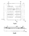
- a coating film 41 could be formed between the portions of the mask 40 as shown in Fig.3B.
- a numeral reference 43 denotes a substrate having the structure having the barrier 3 and the other regions formed beneath it.
- the improvement in crystallizability of the amorphous Si film proceeds toward the center from the both sides, so that the treatment of the crystal grain boundaries formed in the center portion becomes a problem.
- Concerning this by ensuring that the crystal grain boundaries were present in a portion A between two SRAM cell array forming regions 42 (in other words, by ensuring that the active region was not formed in the region in which the crystal grain boundaries were formed) as shown in Fig. 3A, the Si film containing the crystal grain boundaries is removed when the SRAM cell is formed.
- the SRAM cell could be formed by the same steps as shown in Fig. 2C to Fig. 2F has the following advantages:
- the SRAM cell according to this invention has the following advantages:
- a throughhole is bored for connecting the driving transistors and the transfer transistors to the load transistors, and the throughhole is filled up with a refractory metal, whereby the solid phase growth technique can be used without being adversely affected.
Landscapes
- Semiconductor Memories (AREA)
- Thin Film Transistor (AREA)
- Recrystallisation Techniques (AREA)
Applications Claiming Priority (2)
| Application Number | Priority Date | Filing Date | Title |
|---|---|---|---|
| JP01112499A JP3414662B2 (ja) | 1999-01-19 | 1999-01-19 | Sramセル及びその製造方法 |
| JP1112499 | 1999-01-19 |
Publications (2)
| Publication Number | Publication Date |
|---|---|
| EP1022784A2 true EP1022784A2 (fr) | 2000-07-26 |
| EP1022784A3 EP1022784A3 (fr) | 2002-12-04 |
Family
ID=11769278
Family Applications (1)
| Application Number | Title | Priority Date | Filing Date |
|---|---|---|---|
| EP00300390A Withdrawn EP1022784A3 (fr) | 1999-01-19 | 2000-01-19 | Cellule de SRAM et son procédé de fabrication |
Country Status (6)
| Country | Link |
|---|---|
| US (1) | US6204518B1 (fr) |
| EP (1) | EP1022784A3 (fr) |
| JP (1) | JP3414662B2 (fr) |
| KR (1) | KR100358431B1 (fr) |
| CN (1) | CN1238902C (fr) |
| TW (1) | TW451478B (fr) |
Cited By (2)
| Publication number | Priority date | Publication date | Assignee | Title |
|---|---|---|---|---|
| EP1624487A3 (fr) * | 2004-08-04 | 2007-10-03 | Samsung Electronics Co, Ltd | Dispositif semi-conducteur ayant des transistors à effet de champ empilés verticalement et son procédé de fabrication |
| US10658389B2 (en) | 2014-05-30 | 2020-05-19 | Semiconductor Energy Laboratory Co., Ltd. | Semiconductor device, manufacturing method thereof, and electronic device |
Families Citing this family (20)
| Publication number | Priority date | Publication date | Assignee | Title |
|---|---|---|---|---|
| JP2001168038A (ja) * | 1999-12-10 | 2001-06-22 | Sony Corp | 単結晶シリコン層およびそのエピタキシャル成長方法ならびに半導体装置 |
| US6548389B2 (en) * | 2000-04-03 | 2003-04-15 | Matsushita Electric Industrial Co., Ltd. | Semiconductor device and method for fabricating the same |
| KR100418089B1 (ko) * | 2001-06-21 | 2004-02-11 | 주식회사 하이닉스반도체 | 반도체 소자의 박막 트랜지스터 제조 방법 |
| US6670642B2 (en) | 2002-01-22 | 2003-12-30 | Renesas Technology Corporation. | Semiconductor memory device using vertical-channel transistors |
| TWI313062B (en) * | 2002-09-13 | 2009-08-01 | Ind Tech Res Inst | Method for producing active plastic panel displayers |
| US20040211661A1 (en) * | 2003-04-23 | 2004-10-28 | Da Zhang | Method for plasma deposition of a substrate barrier layer |
| JP2005175415A (ja) * | 2003-12-05 | 2005-06-30 | Taiwan Semiconductor Manufacturing Co Ltd | 集積回路デバイスとその製造方法 |
| US6876040B1 (en) * | 2003-12-12 | 2005-04-05 | International Business Machines Corporation | Dense SRAM cells with selective SOI |
| KR100615085B1 (ko) | 2004-01-12 | 2006-08-22 | 삼성전자주식회사 | 노드 콘택 구조체들, 이를 채택하는 반도체소자들, 이를채택하는 에스램 셀들 및 이를 제조하는 방법들 |
| KR100678462B1 (ko) | 2004-11-16 | 2007-02-02 | 삼성전자주식회사 | 단결정 박막 트랜지스터들을 갖는 반도체 집적회로 소자들및 그 제조방법들 |
| KR100566675B1 (ko) | 2004-12-14 | 2006-03-31 | 삼성전자주식회사 | 반도체 장치와 그 제조 방법 |
| KR100594321B1 (ko) * | 2005-02-14 | 2006-06-30 | 삼성전자주식회사 | 소스/드레인에의 접촉 면적을 개선한 트랜지스터 및 제조방법 |
| KR100684894B1 (ko) | 2005-04-18 | 2007-02-20 | 삼성전자주식회사 | 적층된 트랜지스터들을 구비하는 반도체 장치의 형성 방법 |
| US7968394B2 (en) * | 2005-12-16 | 2011-06-28 | Freescale Semiconductor, Inc. | Transistor with immersed contacts and methods of forming thereof |
| KR100861796B1 (ko) * | 2007-01-18 | 2008-10-08 | 주식회사 테라세미콘 | 반도체 소자의 배선 형성 방법 |
| JP5236676B2 (ja) * | 2010-03-18 | 2013-07-17 | ルネサスエレクトロニクス株式会社 | スタティック・ランダム・アクセス・メモリ |
| KR20130068484A (ko) * | 2011-12-15 | 2013-06-26 | 에스케이하이닉스 주식회사 | 저항성 메모리 장치 및 그 제조방법 |
| JP7013293B2 (ja) * | 2018-03-19 | 2022-01-31 | キオクシア株式会社 | 半導体記憶装置 |
| WO2020069312A1 (fr) | 2018-09-28 | 2020-04-02 | The Penn State Research Foundation | Procédé pour faire croître des couches cristallines sur des substrats amorphes au moyen de germes de couche bidimensionnelle et atomique |
| CN117858496B (zh) * | 2024-03-07 | 2024-06-07 | 合肥晶合集成电路股份有限公司 | 静态随机存取存储器单元的制备方法 |
Citations (3)
| Publication number | Priority date | Publication date | Assignee | Title |
|---|---|---|---|---|
| US5780939A (en) * | 1992-12-10 | 1998-07-14 | Siemens Aktiengesellschaft | Method and apparatus for determining orders of non-characteristic harmonic currents, and for compensation of the noncharacteristic harmonic currents |
| US5780326A (en) | 1993-05-12 | 1998-07-14 | Micron Technology, Inc. | Fully planarized thin film transistor (TFT) and process to fabricate same |
| EP0862201A2 (fr) | 1997-02-26 | 1998-09-02 | Semiconductor Energy Laboratory Co., Ltd. | Méthode de fabrication d'un transistor à couches minces |
Family Cites Families (7)
| Publication number | Priority date | Publication date | Assignee | Title |
|---|---|---|---|---|
| JPH02143414A (ja) | 1988-11-24 | 1990-06-01 | Agency Of Ind Science & Technol | 単結晶膜の形成方法 |
| JPH05275652A (ja) * | 1992-01-30 | 1993-10-22 | Sony Corp | ポリシリコン薄膜トランジスタを備えるスタック型トランジスタ及びその製造方法 |
| JPH08204029A (ja) * | 1995-01-23 | 1996-08-09 | Mitsubishi Electric Corp | 半導体装置およびその製造方法 |
| JP3216861B2 (ja) | 1995-04-10 | 2001-10-09 | シャープ株式会社 | 多結晶シリコン膜の形成方法および薄膜トランジスタの製造方法 |
| US5547892A (en) * | 1995-04-27 | 1996-08-20 | Taiwan Semiconductor Manufacturing Company | Process for forming stacked contacts and metal contacts on static random access memory having thin film transistors |
| US5770482A (en) * | 1996-10-08 | 1998-06-23 | Advanced Micro Devices, Inc. | Multi-level transistor fabrication method with a patterned upper transistor substrate and interconnection thereto |
| US5949092A (en) * | 1997-08-01 | 1999-09-07 | Advanced Micro Devices, Inc. | Ultra-high-density pass gate using dual stacked transistors having a gate structure with planarized upper surface in relation to interlayer insulator |
-
1999
- 1999-01-19 JP JP01112499A patent/JP3414662B2/ja not_active Expired - Fee Related
-
2000
- 2000-01-19 CN CNB001011251A patent/CN1238902C/zh not_active Expired - Fee Related
- 2000-01-19 TW TW089100817A patent/TW451478B/zh not_active IP Right Cessation
- 2000-01-19 EP EP00300390A patent/EP1022784A3/fr not_active Withdrawn
- 2000-01-19 KR KR1020000002406A patent/KR100358431B1/ko not_active Expired - Fee Related
- 2000-01-19 US US09/487,258 patent/US6204518B1/en not_active Expired - Fee Related
Patent Citations (3)
| Publication number | Priority date | Publication date | Assignee | Title |
|---|---|---|---|---|
| US5780939A (en) * | 1992-12-10 | 1998-07-14 | Siemens Aktiengesellschaft | Method and apparatus for determining orders of non-characteristic harmonic currents, and for compensation of the noncharacteristic harmonic currents |
| US5780326A (en) | 1993-05-12 | 1998-07-14 | Micron Technology, Inc. | Fully planarized thin film transistor (TFT) and process to fabricate same |
| EP0862201A2 (fr) | 1997-02-26 | 1998-09-02 | Semiconductor Energy Laboratory Co., Ltd. | Méthode de fabrication d'un transistor à couches minces |
Non-Patent Citations (5)
| Title |
|---|
| BERNING G.L.P. ET AL: "Diffusion of Nickel in Silicon below 475°C", THIN SOLID FILMS, vol. 55, 15 December 1978 (1978-12-15), pages 473 - 482, XP009094315 * |
| BONZEL H.P.: "Diffusion of Nickel in Silicon", PHYS. STAT. SOL., vol. 20, 1967, pages 493 - 504, XP009094311 * |
| KITAGAWA H. ET AL: "Electrical Properties of Nickel in Silicon", JOURNAL OF ELECTRONIC MATERIALS, vol. 20, no. 6, June 1991 (1991-06-01), pages 441 - 447, XP009094410 * |
| LEE S.-W. ET AL: "Low Temperature Poly-Si Thin-Film Transistor Fabrication by Metal-Induced Lateral Crystallization", IEEE ELECTRON DEVICE LETTERS, vol. 17, no. 4, April 1996 (1996-04-01), pages 160 - 162, XP000584761 * |
| SUBRAMANIAN V. ET AL: "High-Performance Germanium-Seeded Laterally Crystallized TFT's for Vertical Device Integration", IEEE TRANSACTIONS ON ELECTRON DEVICES, vol. 45, no. 9, September 1998 (1998-09-01), pages 1934 - 1939, XP011016674 * |
Cited By (4)
| Publication number | Priority date | Publication date | Assignee | Title |
|---|---|---|---|---|
| EP1624487A3 (fr) * | 2004-08-04 | 2007-10-03 | Samsung Electronics Co, Ltd | Dispositif semi-conducteur ayant des transistors à effet de champ empilés verticalement et son procédé de fabrication |
| US10658389B2 (en) | 2014-05-30 | 2020-05-19 | Semiconductor Energy Laboratory Co., Ltd. | Semiconductor device, manufacturing method thereof, and electronic device |
| US11282860B2 (en) | 2014-05-30 | 2022-03-22 | Semiconductor Energy Laboratory Co., Ltd. | Semiconductor device, manufacturing method thereof, and electronic device |
| US12495615B2 (en) | 2014-05-30 | 2025-12-09 | Semiconductor Energy Laboratory Co., Ltd. | Semiconductor device, manufacturing method thereof, and electronic device |
Also Published As
| Publication number | Publication date |
|---|---|
| KR20000053530A (ko) | 2000-08-25 |
| TW451478B (en) | 2001-08-21 |
| JP2000208644A (ja) | 2000-07-28 |
| KR100358431B1 (ko) | 2002-10-25 |
| US6204518B1 (en) | 2001-03-20 |
| EP1022784A3 (fr) | 2002-12-04 |
| CN1261207A (zh) | 2000-07-26 |
| CN1238902C (zh) | 2006-01-25 |
| JP3414662B2 (ja) | 2003-06-09 |
Similar Documents
| Publication | Publication Date | Title |
|---|---|---|
| US6204518B1 (en) | SRAM cell and its fabrication process | |
| US6717202B2 (en) | HSG semiconductor capacitor with migration inhibition layer | |
| US5334862A (en) | Thin film transistor (TFT) loads formed in recessed plugs | |
| US5475240A (en) | Contact structure of an interconnection layer for a semiconductor device and a multilayer interconnection SRAM | |
| US7316954B2 (en) | Methods of fabricating integrated circuit devices that utilize doped poly-Si1−xGex conductive plugs as interconnects | |
| US6335250B1 (en) | Semiconductor device and method for the manufacture thereof | |
| EP0242623B1 (fr) | Dispositif semi-conducteur MOS et son procédé de fabrication | |
| US5330929A (en) | Method of making a six transistor static random access memory cell | |
| US5675176A (en) | Semiconductor device and a method for manufacturing the same | |
| US20010017392A1 (en) | Vertical transport MOSFETs and method for making the same | |
| US5536962A (en) | Semiconductor device having a buried channel transistor | |
| KR20040003082A (ko) | 반도체 장치 및 그의 제조방법 | |
| TWI413217B (zh) | 具矽鍺之可程式熔線 | |
| US5497022A (en) | Semiconductor device and a method of manufacturing thereof | |
| US6271064B2 (en) | Thin film transistor and method of manufacturing the same | |
| US5374572A (en) | Method of forming a transistor having an offset channel section | |
| KR100255014B1 (ko) | 고용융점의 금속을 포함하는 고저항 소자를 갖는 반도체 장치 | |
| US6281060B1 (en) | Method of manufacturing a semiconductor device containing a BiCMOS circuit | |
| EP0405063A2 (fr) | FET à grille isolée à structure SOi | |
| JP3388195B2 (ja) | 半導体装置及びその製造方法 | |
| US5604359A (en) | Parasitic PNP transistor with crystal defect layer in the emitter region | |
| KR100207809B1 (ko) | 반도체 장치 및 그의 제조방법 | |
| JP2621820B2 (ja) | スタティック型メモリセル | |
| JP2739849B2 (ja) | 半導体集積回路の製造方法 | |
| KR960015786B1 (ko) | 반도체장치 및 그의 제조방법 |
Legal Events
| Date | Code | Title | Description |
|---|---|---|---|
| PUAI | Public reference made under article 153(3) epc to a published international application that has entered the european phase |
Free format text: ORIGINAL CODE: 0009012 |
|
| AK | Designated contracting states |
Kind code of ref document: A2 Designated state(s): AT BE CH CY DE DK ES FI FR GB GR IE IT LI LU MC NL PT SE |
|
| AX | Request for extension of the european patent |
Free format text: AL;LT;LV;MK;RO;SI |
|
| PUAL | Search report despatched |
Free format text: ORIGINAL CODE: 0009013 |
|
| AK | Designated contracting states |
Kind code of ref document: A3 Designated state(s): AT BE CH CY DE DK ES FI FR GB GR IE IT LI LU MC NL PT SE |
|
| AX | Request for extension of the european patent |
Free format text: AL;LT;LV;MK;RO;SI |
|
| RIC1 | Information provided on ipc code assigned before grant |
Free format text: 7H 01L 21/8244 A, 7H 01L 21/20 B, 7H 01L 21/336 B |
|
| RAP1 | Party data changed (applicant data changed or rights of an application transferred) |
Owner name: SHARP KABUSHIKI KAISHA Owner name: SEMICONDUCTOR ENERGY LABORATORY CO., LTD. |
|
| RAP1 | Party data changed (applicant data changed or rights of an application transferred) |
Owner name: SEMICONDUCTOR ENERGY LABORATORY CO., LTD. Owner name: SHARP KABUSHIKI KAISHA |
|
| 17P | Request for examination filed |
Effective date: 20030507 |
|
| RAP1 | Party data changed (applicant data changed or rights of an application transferred) |
Owner name: SEMICONDUCTOR ENERGY LABORATORY CO., LTD. Owner name: SHARP KABUSHIKI KAISHA |
|
| AKX | Designation fees paid |
Designated state(s): DE FR GB IT NL |
|
| RAP1 | Party data changed (applicant data changed or rights of an application transferred) |
Owner name: SHARP KABUSHIKI KAISHA Owner name: SEMICONDUCTOR ENERGY LABORATORY CO., LTD. |
|
| STAA | Information on the status of an ep patent application or granted ep patent |
Free format text: STATUS: THE APPLICATION IS DEEMED TO BE WITHDRAWN |
|
| 18D | Application deemed to be withdrawn |
Effective date: 20130801 |