EP1032027A2 - Procédé de formation d'un substrat assemblé comprenant une zone planaire de piégeage intrinsèque et substrat ainsi fabriqué - Google Patents
Procédé de formation d'un substrat assemblé comprenant une zone planaire de piégeage intrinsèque et substrat ainsi fabriqué Download PDFInfo
- Publication number
- EP1032027A2 EP1032027A2 EP00101783A EP00101783A EP1032027A2 EP 1032027 A2 EP1032027 A2 EP 1032027A2 EP 00101783 A EP00101783 A EP 00101783A EP 00101783 A EP00101783 A EP 00101783A EP 1032027 A2 EP1032027 A2 EP 1032027A2
- Authority
- EP
- European Patent Office
- Prior art keywords
- semiconductor material
- layer
- wafer
- monocrystalline semiconductor
- zone
- Prior art date
- Legal status (The legal status is an assumption and is not a legal conclusion. Google has not performed a legal analysis and makes no representation as to the accuracy of the status listed.)
- Withdrawn
Links
Images


Classifications
-
- H—ELECTRICITY
- H10—SEMICONDUCTOR DEVICES; ELECTRIC SOLID-STATE DEVICES NOT OTHERWISE PROVIDED FOR
- H10P—GENERIC PROCESSES OR APPARATUS FOR THE MANUFACTURE OR TREATMENT OF DEVICES COVERED BY CLASS H10
- H10P36/00—Gettering within semiconductor bodies
- H10P36/03—Gettering within semiconductor bodies within silicon bodies
- H10P36/07—Gettering within semiconductor bodies within silicon bodies of silicon-on-insulator structures
-
- H—ELECTRICITY
- H10—SEMICONDUCTOR DEVICES; ELECTRIC SOLID-STATE DEVICES NOT OTHERWISE PROVIDED FOR
- H10P—GENERIC PROCESSES OR APPARATUS FOR THE MANUFACTURE OR TREATMENT OF DEVICES COVERED BY CLASS H10
- H10P90/00—Preparation of wafers not covered by a single main group of this subclass, e.g. wafer reinforcement
- H10P90/19—Preparing inhomogeneous wafers
- H10P90/1904—Preparing vertically inhomogeneous wafers
- H10P90/1906—Preparing SOI wafers
-
- H—ELECTRICITY
- H10—SEMICONDUCTOR DEVICES; ELECTRIC SOLID-STATE DEVICES NOT OTHERWISE PROVIDED FOR
- H10P—GENERIC PROCESSES OR APPARATUS FOR THE MANUFACTURE OR TREATMENT OF DEVICES COVERED BY CLASS H10
- H10P90/00—Preparation of wafers not covered by a single main group of this subclass, e.g. wafer reinforcement
- H10P90/19—Preparing inhomogeneous wafers
- H10P90/1904—Preparing vertically inhomogeneous wafers
- H10P90/1906—Preparing SOI wafers
- H10P90/1914—Preparing SOI wafers using bonding
-
- H—ELECTRICITY
- H10—SEMICONDUCTOR DEVICES; ELECTRIC SOLID-STATE DEVICES NOT OTHERWISE PROVIDED FOR
- H10W—GENERIC PACKAGES, INTERCONNECTIONS, CONNECTORS OR OTHER CONSTRUCTIONAL DETAILS OF DEVICES COVERED BY CLASS H10
- H10W10/00—Isolation regions in semiconductor bodies between components of integrated devices
- H10W10/01—Manufacture or treatment
- H10W10/011—Manufacture or treatment of isolation regions comprising dielectric materials
- H10W10/014—Manufacture or treatment of isolation regions comprising dielectric materials using trench refilling with dielectric materials, e.g. shallow trench isolations
-
- H—ELECTRICITY
- H10—SEMICONDUCTOR DEVICES; ELECTRIC SOLID-STATE DEVICES NOT OTHERWISE PROVIDED FOR
- H10W—GENERIC PACKAGES, INTERCONNECTIONS, CONNECTORS OR OTHER CONSTRUCTIONAL DETAILS OF DEVICES COVERED BY CLASS H10
- H10W10/00—Isolation regions in semiconductor bodies between components of integrated devices
- H10W10/01—Manufacture or treatment
- H10W10/061—Manufacture or treatment using SOI processes together with lateral isolation, e.g. combinations of SOI and shallow trench isolations
-
- H—ELECTRICITY
- H10—SEMICONDUCTOR DEVICES; ELECTRIC SOLID-STATE DEVICES NOT OTHERWISE PROVIDED FOR
- H10W—GENERIC PACKAGES, INTERCONNECTIONS, CONNECTORS OR OTHER CONSTRUCTIONAL DETAILS OF DEVICES COVERED BY CLASS H10
- H10W10/00—Isolation regions in semiconductor bodies between components of integrated devices
- H10W10/10—Isolation regions comprising dielectric materials
- H10W10/17—Isolation regions comprising dielectric materials formed using trench refilling with dielectric materials, e.g. shallow trench isolations
-
- H—ELECTRICITY
- H10—SEMICONDUCTOR DEVICES; ELECTRIC SOLID-STATE DEVICES NOT OTHERWISE PROVIDED FOR
- H10W—GENERIC PACKAGES, INTERCONNECTIONS, CONNECTORS OR OTHER CONSTRUCTIONAL DETAILS OF DEVICES COVERED BY CLASS H10
- H10W10/00—Isolation regions in semiconductor bodies between components of integrated devices
- H10W10/10—Isolation regions comprising dielectric materials
- H10W10/181—Semiconductor-on-insulator [SOI] isolation regions, e.g. buried oxide regions of SOI wafers
-
- Y—GENERAL TAGGING OF NEW TECHNOLOGICAL DEVELOPMENTS; GENERAL TAGGING OF CROSS-SECTIONAL TECHNOLOGIES SPANNING OVER SEVERAL SECTIONS OF THE IPC; TECHNICAL SUBJECTS COVERED BY FORMER USPC CROSS-REFERENCE ART COLLECTIONS [XRACs] AND DIGESTS
- Y10—TECHNICAL SUBJECTS COVERED BY FORMER USPC
- Y10S—TECHNICAL SUBJECTS COVERED BY FORMER USPC CROSS-REFERENCE ART COLLECTIONS [XRACs] AND DIGESTS
- Y10S438/00—Semiconductor device manufacturing: process
- Y10S438/977—Thinning or removal of substrate
Definitions
- the present invention relates to gettering in a semiconductor device and, more particularly, to a process for forming a bonded semiconductor-on-insulator substrate containing a planar intrinsic gettering zone and to a semiconductor device and an integrated circuit formed on the bonded substrate.
- a silicon wafer may be exposed to metallic contaminants such as iron, nickel, zinc, chromium, and the like that may ultimately degrade the final product yield, performance, or reliability. This contamination may occur through contact with stainless steel wafer handlers and tools, diffusion of metallic substances from heater coils or lamps in high temperature processing chambers, or sputter debris dislodging from plasma chamber walls.
- Gettering is a term that refers generally to any mechanism by which contaminating impurities, typically transition metals, are removed from sensitive semiconductor device regions and entrapped in other relatively benign domains of the wafer. Gettering is described in Wolf and Tauber, Silicon Processing in the VLSI Era , Vol.1, 1986, Lattice Press, pp 61-70.
- Gettering typically proceeds in three steps: 1) release of a contaminating element from its originating stable state and locale in the wafer into solid solution in the semiconductor crystal lattice; 2) diffusion of the contaminant through the crystal away from sensitive device structures or areas where susceptible structures are ultimately to be formed; and 3) capture of the contaminants by extended defects such as dislocations or precipitates at a position far enough away from devices to avoid interference with their operation and stable enough to prevent future liberation or discharge into the wafer during ensuing thermal, chemical and plasma treatments.
- Extrinsic gettering entails the use of external means (usually on the wafer back surface) to create damage or stress in the silicon lattice, leading to the creation of extended defects capable of mobile metal capture.
- Examples of extrinsic gettering approaches include: diffused backside phosphorus or arsenic doping to tie up nickel, gold, iron, copper, etc., and mechanical or physical backside wafer damage produced by abrasion, grooving, sandblasting, laser deformation, ion implantation, polysilicon deposition, etc.
- Intrinsic gettering is typically accomplished by the localized capture of impurities at extended defects that exist within the bulk material of the silicon wafer, for example, a Czochralski grown monocrystalline wafer containing interstitial oxygen (5-25 ppma).
- Intrinsic gettering usually involves the supersaturation of a region or zone of the silicon wafer with oxygen that will separate from solid solution and form clusters of silicon dioxide during thermal treatment.
- the stresses resulting from the agglomerate clusters cause stacking faults and dislocation loops that are capable of trapping impurities.
- the clusters must be formed in the bulk of the wafer away from active device sites. Oxygen levels above the precipitation threshold must therefore be avoided in regions where active devices will be later be formed and permanently reside.
- U.S. Patent No. 5,229,305 describes a method for implanting boron, argon, krypton or, preferably, oxygen ions into a polished surface of a semiconductor layer, followed by thermal treatment, to create gettering sites in the layer.
- the polished surface of the semiconductor layer is then bonded to a handle substrate, but does not show implanting silicon ions into the silicon substrate.
- To create a high density gettering zone it requires a large implant dose. Such a dose of non-semiconductor ions would alter the electrical characteristics of the semiconductor substrate.
- gettering techniques are inadequate for use with many desired semiconductor devices.
- the formation of gettering sites by treatment of the back surface of a device is generally unsuited for application to semiconductor-on-insulator structures.
- defects that provide gettering sites are often generated in an indiscriminate, scattered fashion throughout the wafer and may thus adversely affect the performance of a device subsequently formed in the wafer.
- a method for making a bonded semiconductor-on-insulator substrate for integrated circuits that includes a high quality semiconductor device wafer having a smooth surface to promote its bonding integrity to a handle wafer and containing a well-defined, restricted intrinsic gettering zone close to but not detrimentally overlapping sites of devices that are particularly susceptible to metal contamination.
- a semiconductor substrate whose electrical characteristics are substantially unchanged by the formation of a gettering zone therein. The present invention meets these needs.
- the present invention is directed to a method for forming a bonded semiconductor-on-insulator substrate for the fabrication of semiconductor devices and integrated circuits.
- ions of the semiconductor material are implanted to a selected depth in the wafer to form, adjacent to the surface, an amorphous layer of the semiconductor material.
- the layer of amorphous semiconductor material extends to a substantially planar zone disposed at substantially the selected depth and comprising the monocrystalline semiconductor material damaged by lattice defects, i.e., end-of-range implant damage.
- Undamaged material below the selected depth comprises a first layer of the monocrystalline semiconductor material.
- the wafer is heated under conditions effective to convert the amorphous layer to a second layer of the monocrystalline semiconductor material and to coalesce the zone of damaged monocrystalline semiconductor material, thereby forming a substantially planar intrinsic gettering zone of substantially pure semiconductor material that includes active gettering sites disposed at substantially the selected depth.
- the present invention includes a method for forming a bonded semiconductor-on-insulator substrate for semiconductor devices and integrated circuits, said steps of the method comprising a wafer having a monocrystalline semiconductor material, implanting ions of the semiconductor material through a surface of the monocrystalline semiconductor wafer to a selected depth in said wafer, so as to forming adjacent to said surface an amorphous layer of the semiconductor material, said amorphous semiconductor layer extending to a substantially planar zone disposed at substantially said selected depth and comprising monocrystalline semiconductor material damaged by lattice defects, undamaged monocrystalline semiconductor material below said selected depth comprising a first layer of the monocrystalline semiconductor material, heating said wafer under conditions effective to convert said amorphous semiconductor layer to a second layer of the monocrystalline semiconductor material, heating the wafer under conditions effective to coalesce said zone of monocrystalline semiconductor material damaged by lattice defects, thereby forming a substantially planar intrinsic gettering zone comprising substantially pure semiconductor material and including active gettering sites, said gettering zone being disposed substantially at said selected depth
- An insulating bond layer on one surface of a handle wafer is bonded to the surface of the wafer to form a bonded semiconductor-on-insulator substrate comprising a handle wafer, an insulating bond layer, and a device wafer of monocrystalline semiconductor material.
- the device wafer includes a substantially planar intrinsic gettering zone comprising substantially pure semiconductor material and including active gettering sites.
- a bonded semiconductor-on-insulator substrate that includes a wafer comprising two layers of a monocrystalline semiconductor material separated by a planar intrinsic gettering zone that comprises substantially pure semiconductor material and contains active gettering sites.
- the invention also includes a bonded semiconductor-on-insulator substrate for semiconductor devices and integrated circuits, said substrate comprising a wafer comprising a monocrystalline semiconductor material and having a first surface and a second surface, said wafer comprising a first layer of the monocrystalline semiconductor material adjacent to said first surface and a second layer of the monocrystalline semiconductor material adjacent to said second surface, and interposed between said first and second layers of the monocrystalline semiconductor material, a substantially planar intrinsic gettering zone comprising substantially pure semiconductor material and including active gettering sites, an insulating bond layer disposed on said second surface of said wafer; and a handle wafer bonded to said insulating bond layer, and a layer of epitaxial monocrystalline semiconductor material deposited on said second layer of monocrystalline semiconductor material, in which said monocrystalline semiconductor material comprises silicon and said implanted ions comprise silicon ions, and said handle wafer comprises silicon and said insulating bond layer comprises silicon dioxide, with said first layer of monocrystalline semiconductor material has a thickness of about 0.1 ⁇ m to about 0.8 ⁇ m, and
- the bonded substrate of the present invention includes a narrowly restricted gettering zone located in near proximity to device regions, which increases the efficiency of contaminant removal from those regions and facilitates small geometry manufacture. Because the gettering zone comprises substantially pure semiconductor material, its formation affects only the structural characteristics and not the electrical characteristics of the wafer.
- the bonded substrate of the invention is reliably constructed and provides excellent structural stability to devices formed on it over a wide range of processing temperature and conditions.
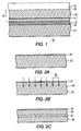
- a bonded substrate 10 of the present invention includes a handle wafer 11 having on one surface 12 an insulating bond layer 13 and a semiconductor device wafer 14 bonded to insulating layer 13.
- Semiconductor device wafer 14 has a first layer 15 of monocrystalline semiconductor material adjacent to insulating layer 13 and a second layer 16 of monocrystalline semiconductor material overlying first layer 15.
- Second monocrystalline semiconductor layer 16 is separated from first monocrystalline semiconductor layer 15 by an intervening substantially planar intrinsic gettering zone 17 comprising gettering sites in the monocrystalline semiconductor material.
- a further optional epitaxial monocrystalline semiconductor layer 18 can be deposited on surface 19 of layer 16.
- FIGS. 2A-F depict the method of the invention for forming the device wafer 14 shown in FIG. 1.
- an oxide layer 21 having a thickness preferably of about 1 nm to about 50 nm is optionally formed on a wafer 22 of monocrystalline semiconductor material.
- the oxide of layer 21 may be a native oxide, a chemically grown oxide, a thermally grown oxide, or a deposited oxide.
- Ions 23 of the semiconductor material at a dose of about to 10 14 to 10 18 ions/cm 2 are implanted, through oxide layer 21 if present, to a selected depth 24 in wafer 22, as shown in FIG. 2B.
- the depth 24 of ion implantation can be controlled by the energy employed; for example, about 185 keV causes implantation of silicon ions at a depth 24 of about 0.4 ⁇ m, while a lower energy of about 90 keV results in a depth 24 of about 0.2 ⁇ m.
- the depth of ion implantation in the monocrystalline semiconductor wafer preferably is about 0.1 ⁇ m to 2.0 ⁇ m, preferably about 0.2 ⁇ m to 0.6 ⁇ m, and the implantation energy preferably is about 50 keV to 250 keV. Ion implantation is well described in Giles, "Ion Implantation," Chapter 8 in Sze, editor, VLSI Technology , Second Edition, McGraw-Hill, Inc., 1988, the disclosure of which is incorporated herein by reference.
- ion implantation results in formation of an amorphous semiconductor layer 25.
- amorphous layer 25 may contain oxygen atoms that originated from layer 21.
- a layer 26 of undamaged monocrystalline semiconductor material is separated from amorphous layer 25 by a substantially planar latent getter zone 27 of monocrystalline semiconductor material containing lattice defects, i.e., end-of-range implant damage.
- Amorphous layer 25 is heated under conditions effective to convert it by solid phase epitaxial annealing to a layer 28 of monocrystalline semiconductor material, as shown in FIG. 2D.
- the annealing of amorphous layer 25 to produce monocrystalline semiconductor layer 28 is achieved by heating to a temperature of about 450°C to 1200°C for about 15 minutes to 8 hours, preferably about 550°C to 620°C for about 2 hours to 6 hours in a non-oxidizing atmosphere such as nitrogen, argon, or hydrogen. Annealing removes from layer 28 sufficient oxygen to preclude the formation of defect sites.
- gettering zone 17 comprises substantially pure semiconductor material containing dislocations that provide active gettering sites. Because implantation is carried out with ions 23 of the semiconductor material, e.g., silicon ions, no dopants or other contaminants that can affect the electrical properties of the semiconductor wafer 14 are introduced during ion implantation.
- ions 23 of the semiconductor material e.g., silicon ions
- Zone 27 can have an initial thickness of about 0.2 ⁇ m to 0.4 ⁇ m, coalescing to form a gettering zone 17 having a thickness of about 0.05 ⁇ m to about 0.2 ⁇ m, preferably about 0.1 ⁇ m.
- First monocrystalline semiconductor layer 15 has a thickness of about 0.1 ⁇ m to about 0.8 ⁇ m, preferably about 0.2 ⁇ m to about 0.4 ⁇ m.
- Second monocrystalline semiconductor layer 16, which is much thicker than layer 15, can have a thickness of 100 ⁇ m or greater prior to being thinned to a desired final thickness of about 0.2 ⁇ m to 20 ⁇ m.
- FIG. 2F Removal of oxide layer 21, if present, produces device wafer 14, as shown in FIG. 2F. It should be noted that the structure of wafer 14 as shown in Fig. 2F is inverted relative to its orientation in FIG. 1.
- FIG. 3 is a schematic representation of the formation of the bonded semiconductor-on-insulator substrate of the present invention by inverting device wafer 14, as shown in FIG. 2F, and bonding it to insulating bond layer 13 on handle wafer 11. Following bonding of wafer 14 to layer 12, thick second monocrystalline semiconductor layer 16 can be thinned to a desired thickness. An epitaxial monocrystalline semiconductor layer 18 can be deposited on thinned layer 16, as shown in FIG. 1, and active devices can be fabricated within epitaxial layer 18.
- the planar gettering zone 17 can be precisely positioned at a depth 24 within device wafer 14.
- the thickness of second monocrystalline semiconductor layer 16 can be controlled by chemical or mechanical material removal means, including etching, lapping, grinding, and polishing.
- gettering zone 17 can also be precisely positioned with respect to devices formed on the surface 19 of layer 16 or in epitaxial layer 18.
- the method of the present invention is applicable to any substrate having a semiconductor-on-insulator structure.
- the semiconductor material comprising device wafer 14 is monocrystalline silicon, in which gettering zone 17 is produced by implanting silicon ions 23 through a layer 22 of silicon dioxide.
- Semiconductor material comprising device wafer 14 can further be germanium, and gettering zone 17 can be produced by implanting germanium ions 23 through a layer 22 of germanium oxide.
- Handle wafer 11 can be formed from a metal, an insulator, silicon carbide, polysilicon or, preferably, monocrystalline silicon.
- Insulating bond layer can be formed of any insulating material but preferably comprises silicon dioxide.
- the method of the present invention is especially useful for forming silicon-on-insulator (SOI) bonded substrates on which semiconductor devices and integrated circuits can be fabricated.
- SOI silicon-on-insulator
- FIG. 4 schematically depicts the cross-section of a bipolar junction transistor (BJT) 40 formed in an epitaxial layer 18 formed on a bonded SOI substrate 10 containing a planar intrinsic gettering zone 17 in accordance with the present invention.
- Transistor 40 includes an emitter diffusion 42, a base diffusion 44, and a collector sinker diffusion 46.
- the polarity of emitter diffusion 42 and sinker diffusion 46 are the same, i.e., n or p, the polarity of base diffusion 44 being the opposite, i.e., p or n.
- Sinker diffusion 46 is connected to a buried layer 43. Insulating layers 48, 49, 50 isolate the respective metal contacts 52, 54, 56 for emitter, base, and sinker diffusions 42, 44, 46.
- Surface insulator 51 protects an interconnect metal line 58 and otherwise seals the surface of transistor 40.
- Lateral isolation trenches 60,61 which have oxide sidewalls and are filled with polysilicon, extend from the surface of transistor 40 to buried oxide insulating layer 13 and serve to isolate transistor 40 from adjacent devices.
- resistors In addition to BJTs, many other types of devices can be constructed on the bonded substrate of the present invention: resistors, capacitors, diodes, field effect transistors (FETs), including junction and MOSFETs, thyristors, and the like.
- FETs field effect transistors
- a method for forming a bonded semiconductor-on-insulator substrate for the fabrication of semiconductor devices and integrated circuits a surface of a wafer of a monocrystalline semiconductor material is implanted with ions of the semiconductor material a to a selected depth in the wafer to form, adjacent to the surface, an amorphous layer of the semiconductor material.
- the layer of amorphous semiconductor material extends to a substantially planar zone disposed at substantially the selected depth and comprising the monocrystalline semiconductor material damaged by lattice defects, i.e., end-of-range implant damage. Undamaged material below the selected depth comprises a first layer of the monocrystalline semiconductor material.
- the wafer is heated under conditions effective to convert the amorphous layer to a second layer of the monocrystalline semiconductor material and to coalesce the zone of damaged monocrystalline semiconductor material, thereby forming a substantially planar intrinsic gettering zone of substantially pure semiconductor material that includes active gettering sites disposed at substantially the selected depth.
- An insulating bond layer on one surface of a handle wafer is bonded to the surface of the wafer to form a bonded semiconductor-on-insulator substrate comprising a handle wafer, an insulating bond layer, and a device wafer of monocrystalline semiconductor material.
Landscapes
- Element Separation (AREA)
- Recrystallisation Techniques (AREA)
- Bipolar Transistors (AREA)
Applications Claiming Priority (2)
| Application Number | Priority Date | Filing Date | Title |
|---|---|---|---|
| US255231 | 1999-02-22 | ||
| US09/255,231 US6255195B1 (en) | 1999-02-22 | 1999-02-22 | Method for forming a bonded substrate containing a planar intrinsic gettering zone and substrate formed by said method |
Publications (2)
| Publication Number | Publication Date |
|---|---|
| EP1032027A2 true EP1032027A2 (fr) | 2000-08-30 |
| EP1032027A3 EP1032027A3 (fr) | 2004-11-24 |
Family
ID=22967415
Family Applications (1)
| Application Number | Title | Priority Date | Filing Date |
|---|---|---|---|
| EP00101783A Withdrawn EP1032027A3 (fr) | 1999-02-22 | 2000-01-28 | Procédé de formation d'un substrat assemblé comprenant une zone planaire de piégeage intrinsèque et substrat ainsi fabriqué |
Country Status (3)
| Country | Link |
|---|---|
| US (3) | US6255195B1 (fr) |
| EP (1) | EP1032027A3 (fr) |
| JP (1) | JP2000260777A (fr) |
Cited By (6)
| Publication number | Priority date | Publication date | Assignee | Title |
|---|---|---|---|---|
| US6534381B2 (en) * | 1999-01-08 | 2003-03-18 | Silicon Genesis Corporation | Method for fabricating multi-layered substrates |
| KR100571572B1 (ko) * | 2000-09-06 | 2006-04-14 | 주식회사 실트론 | 금속 불순물 제거 능력을 향상시킨 접합 에스오아이웨이퍼 제조 방법 |
| WO2007132266A1 (fr) * | 2006-05-11 | 2007-11-22 | X-Fab Semiconductor Foundries Ag | Perfectionnements dans le traitement de semiconducteur |
| EP1710830A3 (fr) * | 2001-06-22 | 2007-11-28 | MEMC Electronic Materials, Inc. | Structure silicium sur isolant a getter intrinseque |
| US7837792B2 (en) | 1995-08-02 | 2010-11-23 | Semiconductor Energy Laboratory Co., Ltd. | Method for manufacturing semiconductor device |
| EP2207194A4 (fr) * | 2007-10-22 | 2013-01-23 | Denso Corp | DISPOSITIF SEMI-CONDUCTEUR DE STRUCTURE SOI (Silicium sur isolant), ET SON PROCÉDÉ DE FABRICATION |
Families Citing this family (46)
| Publication number | Priority date | Publication date | Assignee | Title |
|---|---|---|---|---|
| US7166500B2 (en) * | 1997-10-21 | 2007-01-23 | Semiconductor Energy Laboratory Co., Ltd. | Method of manufacturing a semiconductor device |
| US6199533B1 (en) * | 1999-02-01 | 2001-03-13 | Cummins Engine Company, Inc. | Pilot valve controlled three-way fuel injection control valve assembly |
| US6255195B1 (en) * | 1999-02-22 | 2001-07-03 | Intersil Corporation | Method for forming a bonded substrate containing a planar intrinsic gettering zone and substrate formed by said method |
| US6362075B1 (en) * | 1999-06-30 | 2002-03-26 | Harris Corporation | Method for making a diffused back-side layer on a bonded-wafer with a thick bond oxide |
| US6352909B1 (en) * | 2000-01-06 | 2002-03-05 | Silicon Wafer Technologies, Inc. | Process for lift-off of a layer from a substrate |
| US6573160B2 (en) * | 2000-05-26 | 2003-06-03 | Motorola, Inc. | Method of recrystallizing an amorphous region of a semiconductor |
| US7045444B2 (en) * | 2000-12-19 | 2006-05-16 | Semiconductor Energy Laboratory Co., Ltd. | Method of manufacturing semiconductor device that includes selectively adding a noble gas element |
| US6858480B2 (en) | 2001-01-18 | 2005-02-22 | Semiconductor Energy Laboratory Co., Ltd. | Method of manufacturing semiconductor device |
| TWI221645B (en) | 2001-01-19 | 2004-10-01 | Semiconductor Energy Lab | Method of manufacturing a semiconductor device |
| US7115453B2 (en) * | 2001-01-29 | 2006-10-03 | Semiconductor Energy Laboratory Co., Ltd. | Semiconductor device and manufacturing method of the same |
| JP2002231627A (ja) | 2001-01-30 | 2002-08-16 | Semiconductor Energy Lab Co Ltd | 光電変換装置の作製方法 |
| US7141822B2 (en) * | 2001-02-09 | 2006-11-28 | Semiconductor Energy Laboratory Co., Ltd. | Semiconductor device and method for manufacturing the same |
| JP5088993B2 (ja) | 2001-02-16 | 2012-12-05 | 株式会社半導体エネルギー研究所 | 半導体装置の作製方法 |
| JP4993810B2 (ja) | 2001-02-16 | 2012-08-08 | 株式会社半導体エネルギー研究所 | 半導体装置の作製方法 |
| US6670259B1 (en) * | 2001-02-21 | 2003-12-30 | Advanced Micro Devices, Inc. | Inert atom implantation method for SOI gettering |
| JP4718700B2 (ja) | 2001-03-16 | 2011-07-06 | 株式会社半導体エネルギー研究所 | 半導体装置の作製方法 |
| US7052943B2 (en) | 2001-03-16 | 2006-05-30 | Semiconductor Energy Laboratory Co., Ltd. | Method of manufacturing a semiconductor device |
| US6812081B2 (en) * | 2001-03-26 | 2004-11-02 | Semiconductor Energy Laboratory Co.,.Ltd. | Method of manufacturing semiconductor device |
| AU2002337297A1 (en) * | 2001-10-23 | 2003-05-06 | Cambridge Semiconductor Limited | Lateral semiconductor-on-insulator structure and corresponding manufacturing methods |
| TW200406811A (en) * | 2002-06-03 | 2004-05-01 | Tien-Hsi Lee | Transferring method of a layer onto a substrate |
| FR2845518B1 (fr) * | 2002-10-07 | 2005-10-14 | Commissariat Energie Atomique | Realisation d'un substrat semiconducteur demontable et obtention d'un element semiconducteur |
| US7374976B2 (en) | 2002-11-22 | 2008-05-20 | Semiconductor Energy Laboratory Co., Ltd. | Method for fabricating thin film transistor |
| US20040259321A1 (en) * | 2003-06-19 | 2004-12-23 | Mehran Aminzadeh | Reducing processing induced stress |
| JP2007505477A (ja) * | 2003-07-23 | 2007-03-08 | エーエスエム アメリカ インコーポレイテッド | シリコン−オン−インシュレーター構造及びバルク基板に対するSiGeの堆積 |
| JP2005051040A (ja) * | 2003-07-29 | 2005-02-24 | Matsushita Electric Ind Co Ltd | 半導体装置の製造方法及び半導体基板 |
| US7625808B2 (en) * | 2003-09-01 | 2009-12-01 | Sumco Corporation | Method for manufacturing bonded wafer |
| FR2865574B1 (fr) | 2004-01-26 | 2006-04-07 | Soitec Silicon On Insulator | Procede de fabrication d'un substrat demontable |
| US7442992B2 (en) * | 2004-05-19 | 2008-10-28 | Sumco Corporation | Bonded SOI substrate, and method for manufacturing the same |
| US7095095B2 (en) * | 2004-06-28 | 2006-08-22 | Micron Technology, Inc. | Semiconductor constructions |
| US7560361B2 (en) * | 2004-08-12 | 2009-07-14 | International Business Machines Corporation | Method of forming gate stack for semiconductor electronic device |
| JP5334354B2 (ja) * | 2005-05-13 | 2013-11-06 | シャープ株式会社 | 半導体装置の製造方法 |
| DE102005026408B3 (de) * | 2005-06-08 | 2007-02-01 | Infineon Technologies Ag | Verfahren zur Herstellung einer Stoppzone in einem Halbleiterkörper und Halbleiterbauelement mit einer Stoppzone |
| EP2012347B1 (fr) * | 2006-04-24 | 2015-03-18 | Shin-Etsu Handotai Co., Ltd. | Procede de fabrication d'une plaquette soi |
| JP2010508676A (ja) * | 2006-11-02 | 2010-03-18 | アイメック | 半導体デバイス層からの不純物の除去 |
| US7763502B2 (en) * | 2007-06-22 | 2010-07-27 | Semiconductor Energy Laboratory Co., Ltd | Semiconductor substrate, method for manufacturing semiconductor substrate, semiconductor device, and electronic device |
| US8101501B2 (en) * | 2007-10-10 | 2012-01-24 | Semiconductor Energy Laboratory Co., Ltd. | Method of manufacturing semiconductor device |
| KR101594335B1 (ko) * | 2007-12-03 | 2016-02-16 | 가부시키가이샤 한도오따이 에네루기 켄큐쇼 | 반도체 장치 및 그 제조 방법 |
| KR101063690B1 (ko) * | 2008-11-21 | 2011-09-14 | 주식회사 동부하이텍 | 반도체 소자 및 그 제조 방법 |
| US7967936B2 (en) * | 2008-12-15 | 2011-06-28 | Twin Creeks Technologies, Inc. | Methods of transferring a lamina to a receiver element |
| US8187983B2 (en) * | 2009-04-16 | 2012-05-29 | Micron Technology, Inc. | Methods for fabricating semiconductor components using thinning and back side laser processing |
| US8815641B2 (en) * | 2010-01-29 | 2014-08-26 | Soitec | Diamond SOI with thin silicon nitride layer and related methods |
| US8476150B2 (en) | 2010-01-29 | 2013-07-02 | Intersil Americas Inc. | Methods of forming a semiconductor device |
| FR2980636B1 (fr) * | 2011-09-22 | 2016-01-08 | St Microelectronics Rousset | Protection d'un dispositif electronique contre une attaque laser en face arriere, et support semiconducteur correspondant |
| US9627249B2 (en) * | 2015-09-17 | 2017-04-18 | Taiwan Semiconductor Manufacturing Co., Ltd. | Semiconductor structure and method for manufacturing the same |
| JP6903532B2 (ja) | 2017-09-20 | 2021-07-14 | キオクシア株式会社 | 半導体装置およびその製造方法 |
| DE112019002418B4 (de) * | 2018-06-22 | 2022-06-15 | Ngk Insulators, Ltd. | Verbundener Körper und Elastikwellenelement |
Family Cites Families (15)
| Publication number | Priority date | Publication date | Assignee | Title |
|---|---|---|---|---|
| JPS56105641A (en) * | 1980-01-25 | 1981-08-22 | Mitsubishi Electric Corp | Semiconductor device |
| US4608096A (en) | 1983-04-04 | 1986-08-26 | Monsanto Company | Gettering |
| JPH0237771A (ja) | 1988-07-28 | 1990-02-07 | Fujitsu Ltd | Soi基板 |
| US5266135A (en) * | 1990-02-07 | 1993-11-30 | Harris Corporation | Wafer bonding process employing liquid oxidant |
| FR2681472B1 (fr) * | 1991-09-18 | 1993-10-29 | Commissariat Energie Atomique | Procede de fabrication de films minces de materiau semiconducteur. |
| US5229305A (en) | 1992-02-03 | 1993-07-20 | Motorola, Inc. | Method for making intrinsic gettering sites in bonded substrates |
| JP2908150B2 (ja) * | 1992-11-27 | 1999-06-21 | 日本電気株式会社 | Soi基板構造及びその製造方法 |
| US5661044A (en) * | 1993-11-24 | 1997-08-26 | Lockheed Martin Energy Systems, Inc. | Processing method for forming dislocation-free SOI and other materials for semiconductor use |
| JP3311210B2 (ja) * | 1995-07-28 | 2002-08-05 | 株式会社東芝 | 半導体装置およびその製造方法 |
| JP2743904B2 (ja) * | 1996-02-16 | 1998-04-28 | 日本電気株式会社 | 半導体基板およびこれを用いた半導体装置の製造方法 |
| US6159824A (en) * | 1997-05-12 | 2000-12-12 | Silicon Genesis Corporation | Silicon-on-silicon wafer bonding process using a thin film blister-separation method |
| US5882987A (en) * | 1997-08-26 | 1999-03-16 | International Business Machines Corporation | Smart-cut process for the production of thin semiconductor material films |
| US6083324A (en) * | 1998-02-19 | 2000-07-04 | Silicon Genesis Corporation | Gettering technique for silicon-on-insulator wafers |
| US6255195B1 (en) * | 1999-02-22 | 2001-07-03 | Intersil Corporation | Method for forming a bonded substrate containing a planar intrinsic gettering zone and substrate formed by said method |
| US6368938B1 (en) * | 1999-10-05 | 2002-04-09 | Silicon Wafer Technologies, Inc. | Process for manufacturing a silicon-on-insulator substrate and semiconductor devices on said substrate |
-
1999
- 1999-02-22 US US09/255,231 patent/US6255195B1/en not_active Expired - Lifetime
-
2000
- 2000-01-28 EP EP00101783A patent/EP1032027A3/fr not_active Withdrawn
- 2000-02-01 JP JP2000023611A patent/JP2000260777A/ja active Pending
-
2001
- 2001-05-01 US US09/846,795 patent/US6825532B2/en not_active Expired - Fee Related
-
2004
- 2004-03-29 US US10/811,617 patent/US7052973B2/en not_active Expired - Fee Related
Cited By (6)
| Publication number | Priority date | Publication date | Assignee | Title |
|---|---|---|---|---|
| US7837792B2 (en) | 1995-08-02 | 2010-11-23 | Semiconductor Energy Laboratory Co., Ltd. | Method for manufacturing semiconductor device |
| US6534381B2 (en) * | 1999-01-08 | 2003-03-18 | Silicon Genesis Corporation | Method for fabricating multi-layered substrates |
| KR100571572B1 (ko) * | 2000-09-06 | 2006-04-14 | 주식회사 실트론 | 금속 불순물 제거 능력을 향상시킨 접합 에스오아이웨이퍼 제조 방법 |
| EP1710830A3 (fr) * | 2001-06-22 | 2007-11-28 | MEMC Electronic Materials, Inc. | Structure silicium sur isolant a getter intrinseque |
| WO2007132266A1 (fr) * | 2006-05-11 | 2007-11-22 | X-Fab Semiconductor Foundries Ag | Perfectionnements dans le traitement de semiconducteur |
| EP2207194A4 (fr) * | 2007-10-22 | 2013-01-23 | Denso Corp | DISPOSITIF SEMI-CONDUCTEUR DE STRUCTURE SOI (Silicium sur isolant), ET SON PROCÉDÉ DE FABRICATION |
Also Published As
| Publication number | Publication date |
|---|---|
| EP1032027A3 (fr) | 2004-11-24 |
| US6255195B1 (en) | 2001-07-03 |
| US20010016399A1 (en) | 2001-08-23 |
| US7052973B2 (en) | 2006-05-30 |
| US6825532B2 (en) | 2004-11-30 |
| JP2000260777A (ja) | 2000-09-22 |
| US20040180512A1 (en) | 2004-09-16 |
Similar Documents
| Publication | Publication Date | Title |
|---|---|---|
| US6255195B1 (en) | Method for forming a bonded substrate containing a planar intrinsic gettering zone and substrate formed by said method | |
| US5229305A (en) | Method for making intrinsic gettering sites in bonded substrates | |
| US5646053A (en) | Method and structure for front-side gettering of silicon-on-insulator substrates | |
| TW564500B (en) | Process for controlling denuded zone dept in an ideal oxygen precipitating silicon wafer | |
| EP0299062B1 (fr) | Procede de production d'ilots de silicium monocristaux minces sur un isolateur | |
| US20190341296A1 (en) | HIGH RESISTIVITY SILICON-ON-INSULATOR SUBSTRATE COMPRISING A CHARGE TRAPPING LAYER FORMED BY He-N2 CO-IMPLANTATION | |
| JPH06236976A (ja) | Soi及びその構成方法 | |
| JP2014512091A (ja) | ハンドルウエハ内に高抵抗率領域を有するシリコン・オン・インシュレータ構造体およびそのような構造体の製法 | |
| JP2746499B2 (ja) | 半導体装置及びその製造方法 | |
| EP2012346B1 (fr) | Procédé de fabrication d'une plaquette soi | |
| US6111325A (en) | Gettering regions and methods of forming gettering regions within a semiconductor wafer | |
| US5897362A (en) | Bonding silicon wafers | |
| US6339011B1 (en) | Method of forming semiconductive active area having a proximity gettering region therein and method of processing a monocrystalline silicon substrate to have a proximity gettering region | |
| JP2002184960A (ja) | Soiウェーハの製造方法及びsoiウェーハ | |
| JPH1032209A (ja) | Soiウエハおよびその製造方法ならびにそのsoiウエハを用いた半導体集積回路装置 | |
| JP2998330B2 (ja) | Simox基板及びその製造方法 | |
| US5362659A (en) | Method for fabricating vertical bipolar junction transistors in silicon bonded to an insulator | |
| JPH09326396A (ja) | 半導体集積回路装置およびその製造方法 | |
| JPH08139295A (ja) | Soi基板 | |
| JP3452123B2 (ja) | Soi基板の製造方法 | |
| US20060131687A1 (en) | Method and structure for implanting bonded substrates for electrical conductivity | |
| RU2149481C1 (ru) | Способ создания структуры - кремний на изоляторе для сбис (варианты) | |
| JP3452122B2 (ja) | Soi基板の製造方法 | |
| JPWO2002097892A1 (ja) | Soi基板 | |
| JPH05152304A (ja) | 半導体基板の製造方法 |
Legal Events
| Date | Code | Title | Description |
|---|---|---|---|
| PUAI | Public reference made under article 153(3) epc to a published international application that has entered the european phase |
Free format text: ORIGINAL CODE: 0009012 |
|
| AK | Designated contracting states |
Kind code of ref document: A2 Designated state(s): AT BE CH CY DE DK ES FI FR GB GR IE IT LI LU MC NL PT SE |
|
| AX | Request for extension of the european patent |
Free format text: AL;LT;LV;MK;RO;SI |
|
| PUAL | Search report despatched |
Free format text: ORIGINAL CODE: 0009013 |
|
| AK | Designated contracting states |
Kind code of ref document: A3 Designated state(s): AT BE CH CY DE DK ES FI FR GB GR IE IT LI LU MC NL PT SE |
|
| AX | Request for extension of the european patent |
Extension state: AL LT LV MK RO SI |
|
| AKX | Designation fees paid |
Designated state(s): DE DK GB IT |
|
| STAA | Information on the status of an ep patent application or granted ep patent |
Free format text: STATUS: THE APPLICATION IS DEEMED TO BE WITHDRAWN |
|
| 18D | Application deemed to be withdrawn |
Effective date: 20050525 |