EP1032043A2 - Dispositif semi-conducteur de mémoire avec lignes de bit entrelacées - Google Patents
Dispositif semi-conducteur de mémoire avec lignes de bit entrelacées Download PDFInfo
- Publication number
- EP1032043A2 EP1032043A2 EP00103078A EP00103078A EP1032043A2 EP 1032043 A2 EP1032043 A2 EP 1032043A2 EP 00103078 A EP00103078 A EP 00103078A EP 00103078 A EP00103078 A EP 00103078A EP 1032043 A2 EP1032043 A2 EP 1032043A2
- Authority
- EP
- European Patent Office
- Prior art keywords
- bit lines
- twist
- bit
- bit line
- lines
- Prior art date
- Legal status (The legal status is an assumption and is not a legal conclusion. Google has not performed a legal analysis and makes no representation as to the accuracy of the status listed.)
- Withdrawn
Links
Images

Classifications
-
- H—ELECTRICITY
- H10—SEMICONDUCTOR DEVICES; ELECTRIC SOLID-STATE DEVICES NOT OTHERWISE PROVIDED FOR
- H10B—ELECTRONIC MEMORY DEVICES
- H10B12/00—Dynamic random access memory [DRAM] devices
- H10B12/30—DRAM devices comprising one-transistor - one-capacitor [1T-1C] memory cells
- H10B12/48—Data lines or contacts therefor
- H10B12/482—Bit lines
-
- G—PHYSICS
- G11—INFORMATION STORAGE
- G11C—STATIC STORES
- G11C7/00—Arrangements for writing information into, or reading information out from, a digital store
- G11C7/18—Bit line organisation; Bit line lay-out
-
- H—ELECTRICITY
- H10—SEMICONDUCTOR DEVICES; ELECTRIC SOLID-STATE DEVICES NOT OTHERWISE PROVIDED FOR
- H10B—ELECTRONIC MEMORY DEVICES
- H10B12/00—Dynamic random access memory [DRAM] devices
- H10B12/30—DRAM devices comprising one-transistor - one-capacitor [1T-1C] memory cells
- H10B12/48—Data lines or contacts therefor
- H10B12/488—Word lines
-
- H—ELECTRICITY
- H10—SEMICONDUCTOR DEVICES; ELECTRIC SOLID-STATE DEVICES NOT OTHERWISE PROVIDED FOR
- H10B—ELECTRONIC MEMORY DEVICES
- H10B12/00—Dynamic random access memory [DRAM] devices
- H10B12/50—Peripheral circuit region structures
-
- H—ELECTRICITY
- H10—SEMICONDUCTOR DEVICES; ELECTRIC SOLID-STATE DEVICES NOT OTHERWISE PROVIDED FOR
- H10W—GENERIC PACKAGES, INTERCONNECTIONS, CONNECTORS OR OTHER CONSTRUCTIONAL DETAILS OF DEVICES COVERED BY CLASS H10
- H10W20/00—Interconnections in chips, wafers or substrates
- H10W20/40—Interconnections external to wafers or substrates, e.g. back-end-of-line [BEOL] metallisations or vias connecting to gate electrodes
- H10W20/41—Interconnections external to wafers or substrates, e.g. back-end-of-line [BEOL] metallisations or vias connecting to gate electrodes characterised by their conductive parts
- H10W20/423—Shielding layers
-
- Y—GENERAL TAGGING OF NEW TECHNOLOGICAL DEVELOPMENTS; GENERAL TAGGING OF CROSS-SECTIONAL TECHNOLOGIES SPANNING OVER SEVERAL SECTIONS OF THE IPC; TECHNICAL SUBJECTS COVERED BY FORMER USPC CROSS-REFERENCE ART COLLECTIONS [XRACs] AND DIGESTS
- Y10—TECHNICAL SUBJECTS COVERED BY FORMER USPC
- Y10S—TECHNICAL SUBJECTS COVERED BY FORMER USPC CROSS-REFERENCE ART COLLECTIONS [XRACs] AND DIGESTS
- Y10S257/00—Active solid-state devices, e.g. transistors, solid-state diodes
- Y10S257/907—Folded bit line dram configuration
Definitions
- the present invention relates to a semiconductor memory device with word lines and bit lines that are guided over a memory cell array, with bit lines with bit line twist in addition to bit lines without bit line twist run and each with a bit line pair Bit line twist Contacts to cross one bit line through the other bit line of the bit line pair in one other level different from the bit line level Has.
- Bit lines are known to be above memory cell arrays with bit line twist and without bit line twist.
- Bit line twist has the advantage that the two are connected by the Twist intersecting bit lines capacitively symmetrical are coupled so that possible interference signals each other cancel.
- the coupling increases from neighboring lines if they are folded or "folded" bit lines.
- the crossing of two bit lines in a twist sets assume that one of the bit lines is spaced and electrically is isolated over the other bit line. This can happen, for example, in such a way that the one bit line in the crossover area to the other bit line Contacts in the word line level is raised, so that in this crossing area the one bit line in the word line level runs while the other bit line on the Bit line level remains.
- Adjacent bit lines should be mutually exclusive if possible affect little, i.e., the electrical coupling between such adjacent bit lines should be as far as possible be reduced. This can basically be done by that the bit lines are at a greater distance and are guided to each other without a twist or crossover. On such a larger distance is inevitable with one increased space requirement for the memory cell array connected.
- Twist introduced the bit lines can now be closer together run, with the inevitably existing capacitive Coupling introduced interference due to each other Pick up twists.
- Semiconductor memory arrangements are currently preferred used in which bit lines in pairs are twist-free and provided with a twist. That is, on two bit lines with a twist are followed by two bit lines without Twist. It has been shown that by such a design the bit lines an optimization with regard to reduction the effects of capacitive coupling due to the Twists of every other bit line pair and simplification the circuit structure due to necessary crossovers for to achieve every second pair with reduced space requirements is.
- a disadvantage of such a semiconductor memory device lies in the fact that in the word line level the individual word lines in different places different Experience neighborhood effects, because only in the area of the bit line pairs with twist the one bit lines with their Contacts are led to the word line level. Kick it so here in an undesirable way different and inhomogeneous Influencing the word lines in the crossover area of the bit lines.
- the further level is advantageously the word line level.
- the bit lines have in the twist-free area a width of about 150 to 250 nm, preferably from 200 to 225 nm, while the bit lines themselves in the twist range 250 to 350 nm, preferably 330 nm, are wide.
- the distance between the bit lines or their contacts and the bit lines is about 150 to 200 nm.
- the dummy contacts have edge elements in the further Level that in the twist area to the contacts of the bit lines adjoin the same electrical "environment", so here different neighborhood effects can be avoided.
- bit lines can be extremely so with high area efficiency homogeneous, electrical and geometrically largely symmetrical be performed so that no problems with edge elements caused in the crossover area.
- the memory cell array located under the bit lines is completely in the area of the crossover or twist regularly, so that there are no additional marginal areas result and the introduction of special edge elements is not required. Due to the narrow routing of the bit lines next to each other there is also a need for space Way kept low.
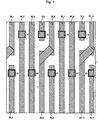
- Fig. 1 shows bit lines BL1 to Bl10, of which the bit lines BL1 and BL2, BL5 and BL6 as well as BL9 and BL10 bit lines are with bit line twist, while the bit lines BL3 and BL4 and BL7 and BL8 represent twist-free bit lines.
- the bit line BL2 crosses the bit line BL1
- bit line BL5 crosses bit line BL6
- bit line LB9 crosses bit line BL10, respectively in a different from the bit line level shown, higher level.
- the bit lines BL1, BL6 and BL10 in a twist or crossover area 1 bit lines BL2 (upper Half is not shown in Fig. 1)
- the bit line BL5 and the bit line BL9 by means of contacts 2 or 3, 4 or 5, 6 in an overlying level raised to higher in this one Level in twist area 1, bit lines BL1 and BL6 or BL10 to cross.
- Fig. 2 is a word line level with word lines WL1 until WL5 shows.
- a memory cell array 7 memory cells, not shown from, for example, a transistor and a capacitor arranged.
- bit line BL5 runs for example from contact 3 in the higher word line level at a distance obliquely over the bit line BL6 in Twist area 1 to return to the bit line level via contact 4 (Fig. 1) to be returned. same for for bit lines BL2 and BL9 with contacts 5 and 6 for example the bit line BL9.
- the word line WL2 has an inhomogeneous in this way "Neighborhood": it borders on the upper contact in FIG. 2 the bit line BL2 and the contacts 3 and 5 of the bit lines BL5 and BL9 on, while in the space between these contacts have a metallization-free space. The same applies to the word line WL3, which is between the contacts 2, 4 and 6 non-contact zones.
- bit lines BL3, BL4 or BL7, BL8, which do not show any crossovers or twists are provided with dummy contacts 8 to 11, i.e. with Contacts that go up from the bit line level (Fig. 1) lead to the word line level (Fig. 2) and end there. On this ensures that the word lines WL2, WL3 show a continuous and homogeneous neighborhood, so that the discontinuities mentioned are avoided.
- the invention thus enables the bit lines to have a high density and thus a maximum electrical space requirement and geometric symmetry, which is under the bitlines lying memory cell array in the twist area 1 completely is regular. There are no additional results Marginal areas, and the introduction of special marginal elements not necessary.
- WL3 instead of the word lines WL2, WL3 other structures can also be provided. Also in In this case, these structures then become homogeneous of contacts 2, 9, 4 and 11 or 8, 3, 10 and 5 optimal influences what is due to the maximum possible symmetry is.
- word lines and the bit lines as well as for the contacts can, for example, aluminum or copper as a material be used. Of course, there are others too Materials can be used.
- Bit lines BL1 to BL10 are approximately in the twist-free range 150 to 250 nm and preferably about 200 to 225 nm wide, while in the twist region 1 they have a width of 250 nm or Can have 350 nm and in particular of about 330 nm.
- the Contacts themselves have a diameter of about 400 nm, while the distance between the bit lines 150 to 200 nm can be.
Landscapes
- Semiconductor Memories (AREA)
- Internal Circuitry In Semiconductor Integrated Circuit Devices (AREA)
Applications Claiming Priority (2)
| Application Number | Priority Date | Filing Date | Title |
|---|---|---|---|
| DE19908428A DE19908428C2 (de) | 1999-02-26 | 1999-02-26 | Halbleiterspeicheranordnung mit Bitleitungs-Twist |
| DE19908428 | 1999-02-26 |
Publications (2)
| Publication Number | Publication Date |
|---|---|
| EP1032043A2 true EP1032043A2 (fr) | 2000-08-30 |
| EP1032043A3 EP1032043A3 (fr) | 2005-08-24 |
Family
ID=7899014
Family Applications (1)
| Application Number | Title | Priority Date | Filing Date |
|---|---|---|---|
| EP00103078A Withdrawn EP1032043A3 (fr) | 1999-02-26 | 2000-02-15 | Dispositif semi-conducteur de mémoire avec lignes de bit entrelacées |
Country Status (6)
| Country | Link |
|---|---|
| US (1) | US6310399B1 (fr) |
| EP (1) | EP1032043A3 (fr) |
| JP (1) | JP4144832B2 (fr) |
| KR (1) | KR100338156B1 (fr) |
| DE (1) | DE19908428C2 (fr) |
| TW (1) | TW463355B (fr) |
Families Citing this family (9)
| Publication number | Priority date | Publication date | Assignee | Title |
|---|---|---|---|---|
| US6326695B1 (en) * | 1998-09-29 | 2001-12-04 | Texas Instruments Incorporated | Twisted bit line structures and method for making same |
| US6686668B2 (en) * | 2001-01-17 | 2004-02-03 | International Business Machines Corporation | Structure and method of forming bitline contacts for a vertical DRAM array using a line bitline contact mask |
| US6768206B2 (en) | 2002-05-07 | 2004-07-27 | Kabushiki Kaisha Toshiba | Organic substrate for flip chip bonding |
| US6721217B2 (en) | 2002-06-27 | 2004-04-13 | Texas Instruments Incorporated | Method for memory sensing |
| DE10308924B3 (de) * | 2003-02-28 | 2004-10-28 | Infineon Technologies Ag | Integrierte Halbleiterschaltung mit einer Vielzahl von Speicherzellen |
| US6717839B1 (en) | 2003-03-31 | 2004-04-06 | Ramtron International Corporation | Bit-line shielding method for ferroelectric memories |
| JP4216270B2 (ja) * | 2004-06-30 | 2009-01-28 | 三星エスディアイ株式会社 | 電子装置、薄膜トランジスタ構造体及びそれを備える平板ディスプレイ装置 |
| JP2009271261A (ja) * | 2008-05-02 | 2009-11-19 | Powerchip Semiconductor Corp | 回路構造とそれを定義するためのフォトマスク |
| KR102171258B1 (ko) | 2014-05-21 | 2020-10-28 | 삼성전자 주식회사 | 반도체 소자 |
Citations (1)
| Publication number | Priority date | Publication date | Assignee | Title |
|---|---|---|---|---|
| EP1030367A2 (fr) | 1999-02-19 | 2000-08-23 | Infineon Technologies AG | Dispositif semi-conducteur avec des lignes conductrices stabilisées |
Family Cites Families (8)
| Publication number | Priority date | Publication date | Assignee | Title |
|---|---|---|---|---|
| JPH0760858B2 (ja) * | 1984-10-26 | 1995-06-28 | 三菱電機株式会社 | 半導体メモリ装置 |
| JPH0666442B2 (ja) * | 1985-03-08 | 1994-08-24 | 三菱電機株式会社 | 半導体メモリ装置 |
| US5144583A (en) * | 1989-01-09 | 1992-09-01 | Kabushiki Kaisha Toshiba | Dynamic semiconductor memory device with twisted bit-line structure |
| JP3241106B2 (ja) * | 1992-07-17 | 2001-12-25 | 株式会社東芝 | ダイナミック型半導体記憶装置及びその製造方法 |
| US5864181A (en) * | 1993-09-15 | 1999-01-26 | Micron Technology, Inc. | Bi-level digit line architecture for high density DRAMs |
| US5770518A (en) * | 1995-04-19 | 1998-06-23 | Advanced Micro Devices, Inc. | Semiconductor device and method of manufacturing without undercutting conductive lines |
| US5866928A (en) * | 1996-07-16 | 1999-02-02 | Micron Technology, Inc. | Single digit line with cell contact interconnect |
| US5821592A (en) * | 1997-06-30 | 1998-10-13 | Siemens Aktiengesellschaft | Dynamic random access memory arrays and methods therefor |
-
1999
- 1999-02-26 DE DE19908428A patent/DE19908428C2/de not_active Expired - Fee Related
-
2000
- 2000-02-15 EP EP00103078A patent/EP1032043A3/fr not_active Withdrawn
- 2000-02-22 TW TW089103055A patent/TW463355B/zh not_active IP Right Cessation
- 2000-02-23 KR KR1020000008769A patent/KR100338156B1/ko not_active Expired - Fee Related
- 2000-02-23 JP JP2000046287A patent/JP4144832B2/ja not_active Expired - Fee Related
- 2000-02-28 US US09/514,268 patent/US6310399B1/en not_active Expired - Lifetime
Patent Citations (1)
| Publication number | Priority date | Publication date | Assignee | Title |
|---|---|---|---|---|
| EP1030367A2 (fr) | 1999-02-19 | 2000-08-23 | Infineon Technologies AG | Dispositif semi-conducteur avec des lignes conductrices stabilisées |
Also Published As
| Publication number | Publication date |
|---|---|
| JP4144832B2 (ja) | 2008-09-03 |
| JP2000252440A (ja) | 2000-09-14 |
| DE19908428A1 (de) | 2000-09-07 |
| TW463355B (en) | 2001-11-11 |
| EP1032043A3 (fr) | 2005-08-24 |
| KR100338156B1 (ko) | 2002-05-24 |
| KR20000058157A (ko) | 2000-09-25 |
| DE19908428C2 (de) | 2000-12-07 |
| US6310399B1 (en) | 2001-10-30 |
Similar Documents
| Publication | Publication Date | Title |
|---|---|---|
| DE69933493T2 (de) | Zugriffsstruktur für hochintegrierten Festwertspeicher | |
| DE69526006T2 (de) | Anordnung mit einem einzigen Verdrillungsgebiet und Verfahren für gepaarte linienförmige Leiter in integrierten Schaltungen | |
| DE10065703B4 (de) | Spaltenauswahltransistoranordnung | |
| DE4433695C2 (de) | Dynamische Halbleiterspeichervorrichtung | |
| DE69834540T2 (de) | Halbleiterspeicher | |
| DE102012019196B4 (de) | Speicherarray mit hierarchischer Bitleitungsstruktur | |
| DE69325133T2 (de) | Halbleiterfestwertspeicher | |
| DE102005010156A1 (de) | Integrierte Schaltung mit Umlenkungsschicht und Anordnung aus gestapelten Einzelschaltkreisen | |
| DE102005056427A1 (de) | Speicherzellenfeld | |
| EP0025130A2 (fr) | Mémoire morte intégrée très dense | |
| DE112020003936B4 (de) | Elektronische Vorrichtung | |
| DE3937068A1 (de) | Dynamische halbleiterspeicheranordnung | |
| DE19908428C2 (de) | Halbleiterspeicheranordnung mit Bitleitungs-Twist | |
| DE10234945B3 (de) | Halbleiterspeicher mit einer Anordnung von Speicherzellen | |
| DE69024167T2 (de) | Halbleiterspeicheranordnung | |
| DE69430600T2 (de) | Zeilenförmiger Farbbildaufnahmesensor mit vermindertem Abstand zwischen Photosensoranordnungen | |
| DE4126050C2 (de) | Anordnung von Wortleitungstreiberstufen in einer Halbleiterspeicheranordnung | |
| DE69020237T2 (de) | Halbleiterspeicheranordnung mit einer Bitleitungsstruktur mit niedrigem Geräusch. | |
| DE60015006T2 (de) | Verbindungsschema für Halbleiter-Speicherbauteil | |
| EP1030311B1 (fr) | Connection de décodeur pour mémoire à longues lignes de bit | |
| DE69832164T2 (de) | Ausleseanordnung für Multibit-Halbleiterspeicheranordnung | |
| DE4105765C2 (de) | Dynamischer Schreib-/Lesespeicher (DRAM) | |
| DE19918932A1 (de) | Halbleiterspeichervorrichtung | |
| DE69422174T2 (de) | Integrierte Schaltung mit Toleranz bei wichtigen Herstellungsfehlern | |
| EP1232528B1 (fr) | Dram avec lignes de bit a deux niveaux de metallisation |
Legal Events
| Date | Code | Title | Description |
|---|---|---|---|
| PUAI | Public reference made under article 153(3) epc to a published international application that has entered the european phase |
Free format text: ORIGINAL CODE: 0009012 |
|
| AK | Designated contracting states |
Kind code of ref document: A2 Designated state(s): AT BE CH CY DE DK ES FI FR GB GR IE IT LI LU MC NL PT SE |
|
| AX | Request for extension of the european patent |
Free format text: AL;LT;LV;MK;RO;SI |
|
| PUAL | Search report despatched |
Free format text: ORIGINAL CODE: 0009013 |
|
| RIC1 | Information provided on ipc code assigned before grant |
Ipc: 7H 01L 21/8242 B Ipc: 7H 01L 23/522 B Ipc: 7H 01L 27/108 A |
|
| AK | Designated contracting states |
Kind code of ref document: A3 Designated state(s): AT BE CH CY DE DK ES FI FR GB GR IE IT LI LU MC NL PT SE |
|
| AX | Request for extension of the european patent |
Extension state: AL LT LV MK RO SI |
|
| 17P | Request for examination filed |
Effective date: 20050908 |
|
| AKX | Designation fees paid |
Designated state(s): DE FR GB IE IT |
|
| 17Q | First examination report despatched |
Effective date: 20080813 |
|
| STAA | Information on the status of an ep patent application or granted ep patent |
Free format text: STATUS: THE APPLICATION IS DEEMED TO BE WITHDRAWN |
|
| 18D | Application deemed to be withdrawn |
Effective date: 20090901 |