EP1032098B1 - Dispositif laser - Google Patents
Dispositif laser Download PDFInfo
- Publication number
- EP1032098B1 EP1032098B1 EP00301521A EP00301521A EP1032098B1 EP 1032098 B1 EP1032098 B1 EP 1032098B1 EP 00301521 A EP00301521 A EP 00301521A EP 00301521 A EP00301521 A EP 00301521A EP 1032098 B1 EP1032098 B1 EP 1032098B1
- Authority
- EP
- European Patent Office
- Prior art keywords
- slot
- energy
- laser
- laser gas
- waveguide
- Prior art date
- Legal status (The legal status is an assumption and is not a legal conclusion. Google has not performed a legal analysis and makes no representation as to the accuracy of the status listed.)
- Expired - Lifetime
Links
- 238000009826 distribution Methods 0.000 claims description 16
- 230000003287 optical effect Effects 0.000 claims description 14
- 238000004519 manufacturing process Methods 0.000 claims description 8
- 239000012141 concentrate Substances 0.000 claims description 6
- 230000005281 excited state Effects 0.000 claims description 4
- 238000005286 illumination Methods 0.000 claims description 4
- 239000000463 material Substances 0.000 claims description 4
- 230000001678 irradiating effect Effects 0.000 claims description 2
- 239000000758 substrate Substances 0.000 claims 5
- 239000011248 coating agent Substances 0.000 claims 1
- 238000000576 coating method Methods 0.000 claims 1
- 230000001902 propagating effect Effects 0.000 claims 1
- 239000007789 gas Substances 0.000 description 54
- 235000012431 wafers Nutrition 0.000 description 28
- 230000005284 excitation Effects 0.000 description 22
- 238000009281 ultraviolet germicidal irradiation Methods 0.000 description 14
- 230000005540 biological transmission Effects 0.000 description 13
- 238000000034 method Methods 0.000 description 11
- 239000004065 semiconductor Substances 0.000 description 9
- 230000015572 biosynthetic process Effects 0.000 description 5
- 230000008569 process Effects 0.000 description 5
- 230000005684 electric field Effects 0.000 description 4
- 238000012360 testing method Methods 0.000 description 4
- 229910052786 argon Inorganic materials 0.000 description 3
- 238000001816 cooling Methods 0.000 description 3
- 229910052743 krypton Inorganic materials 0.000 description 3
- 238000006243 chemical reaction Methods 0.000 description 2
- 230000000694 effects Effects 0.000 description 2
- 238000005530 etching Methods 0.000 description 2
- 230000005283 ground state Effects 0.000 description 2
- 229910052734 helium Inorganic materials 0.000 description 2
- 239000011261 inert gas Substances 0.000 description 2
- 230000007246 mechanism Effects 0.000 description 2
- 239000012071 phase Substances 0.000 description 2
- 238000012545 processing Methods 0.000 description 2
- 230000001737 promoting effect Effects 0.000 description 2
- 125000004429 atom Chemical group 0.000 description 1
- 238000001444 catalytic combustion detection Methods 0.000 description 1
- 239000000919 ceramic Substances 0.000 description 1
- 239000003795 chemical substances by application Substances 0.000 description 1
- 239000000498 cooling water Substances 0.000 description 1
- 238000013461 design Methods 0.000 description 1
- 238000011161 development Methods 0.000 description 1
- 238000010894 electron beam technology Methods 0.000 description 1
- 238000005538 encapsulation Methods 0.000 description 1
- 239000011521 glass Substances 0.000 description 1
- 238000005468 ion implantation Methods 0.000 description 1
- 150000002500 ions Chemical class 0.000 description 1
- 239000004973 liquid crystal related substance Substances 0.000 description 1
- 239000002184 metal Substances 0.000 description 1
- 229910052751 metal Inorganic materials 0.000 description 1
- 150000002739 metals Chemical class 0.000 description 1
- 239000000203 mixture Substances 0.000 description 1
- 238000012986 modification Methods 0.000 description 1
- 230000004048 modification Effects 0.000 description 1
- 229910052754 neon Inorganic materials 0.000 description 1
- 238000009828 non-uniform distribution Methods 0.000 description 1
- 230000010355 oscillation Effects 0.000 description 1
- 230000003647 oxidation Effects 0.000 description 1
- 238000007254 oxidation reaction Methods 0.000 description 1
- 238000004806 packaging method and process Methods 0.000 description 1
- 238000000206 photolithography Methods 0.000 description 1
- 238000005240 physical vapour deposition Methods 0.000 description 1
- 230000005855 radiation Effects 0.000 description 1
- 239000011347 resin Substances 0.000 description 1
- 229920005989 resin Polymers 0.000 description 1
- 238000005389 semiconductor device fabrication Methods 0.000 description 1
- 229910052710 silicon Inorganic materials 0.000 description 1
- 239000010703 silicon Substances 0.000 description 1
- 230000002269 spontaneous effect Effects 0.000 description 1
- 238000004544 sputter deposition Methods 0.000 description 1
- 239000000126 substance Substances 0.000 description 1
- 230000002459 sustained effect Effects 0.000 description 1
- 238000009827 uniform distribution Methods 0.000 description 1
- 238000007740 vapor deposition Methods 0.000 description 1
- 239000012808 vapor phase Substances 0.000 description 1
Images





Classifications
-
- H—ELECTRICITY
- H01—ELECTRIC ELEMENTS
- H01S—DEVICES USING THE PROCESS OF LIGHT AMPLIFICATION BY STIMULATED EMISSION OF RADIATION [LASER] TO AMPLIFY OR GENERATE LIGHT; DEVICES USING STIMULATED EMISSION OF ELECTROMAGNETIC RADIATION IN WAVE RANGES OTHER THAN OPTICAL
- H01S3/00—Lasers, i.e. devices using stimulated emission of electromagnetic radiation in the infrared, visible or ultraviolet wave range
- H01S3/02—Constructional details
- H01S3/03—Constructional details of gas laser discharge tubes
- H01S3/0315—Waveguide lasers
-
- G—PHYSICS
- G03—PHOTOGRAPHY; CINEMATOGRAPHY; ANALOGOUS TECHNIQUES USING WAVES OTHER THAN OPTICAL WAVES; ELECTROGRAPHY; HOLOGRAPHY
- G03F—PHOTOMECHANICAL PRODUCTION OF TEXTURED OR PATTERNED SURFACES, e.g. FOR PRINTING, FOR PROCESSING OF SEMICONDUCTOR DEVICES; MATERIALS THEREFOR; ORIGINALS THEREFOR; APPARATUS SPECIALLY ADAPTED THEREFOR
- G03F7/00—Photomechanical, e.g. photolithographic, production of textured or patterned surfaces, e.g. printing surfaces; Materials therefor, e.g. comprising photoresists; Apparatus specially adapted therefor
- G03F7/70—Microphotolithographic exposure; Apparatus therefor
- G03F7/70383—Direct write, i.e. pattern is written directly without the use of a mask by one or multiple beams
-
- H—ELECTRICITY
- H01—ELECTRIC ELEMENTS
- H01S—DEVICES USING THE PROCESS OF LIGHT AMPLIFICATION BY STIMULATED EMISSION OF RADIATION [LASER] TO AMPLIFY OR GENERATE LIGHT; DEVICES USING STIMULATED EMISSION OF ELECTROMAGNETIC RADIATION IN WAVE RANGES OTHER THAN OPTICAL
- H01S3/00—Lasers, i.e. devices using stimulated emission of electromagnetic radiation in the infrared, visible or ultraviolet wave range
- H01S3/02—Constructional details
- H01S3/03—Constructional details of gas laser discharge tubes
- H01S3/038—Electrodes, e.g. special shape, configuration or composition
- H01S3/0385—Shape
-
- H—ELECTRICITY
- H01—ELECTRIC ELEMENTS
- H01S—DEVICES USING THE PROCESS OF LIGHT AMPLIFICATION BY STIMULATED EMISSION OF RADIATION [LASER] TO AMPLIFY OR GENERATE LIGHT; DEVICES USING STIMULATED EMISSION OF ELECTROMAGNETIC RADIATION IN WAVE RANGES OTHER THAN OPTICAL
- H01S3/00—Lasers, i.e. devices using stimulated emission of electromagnetic radiation in the infrared, visible or ultraviolet wave range
- H01S3/09—Processes or apparatus for excitation, e.g. pumping
- H01S3/097—Processes or apparatus for excitation, e.g. pumping by gas discharge of a gas laser
- H01S3/0975—Processes or apparatus for excitation, e.g. pumping by gas discharge of a gas laser using inductive or capacitive excitation
-
- H—ELECTRICITY
- H01—ELECTRIC ELEMENTS
- H01S—DEVICES USING THE PROCESS OF LIGHT AMPLIFICATION BY STIMULATED EMISSION OF RADIATION [LASER] TO AMPLIFY OR GENERATE LIGHT; DEVICES USING STIMULATED EMISSION OF ELECTROMAGNETIC RADIATION IN WAVE RANGES OTHER THAN OPTICAL
- H01S3/00—Lasers, i.e. devices using stimulated emission of electromagnetic radiation in the infrared, visible or ultraviolet wave range
- H01S3/14—Lasers, i.e. devices using stimulated emission of electromagnetic radiation in the infrared, visible or ultraviolet wave range characterised by the material used as the active medium
- H01S3/22—Gases
- H01S3/223—Gases the active gas being polyatomic, i.e. containing two or more atoms
- H01S3/225—Gases the active gas being polyatomic, i.e. containing two or more atoms comprising an excimer or exciplex
Definitions
- the present invention relates to a laser oscillating apparatus for generating a laser beam by introducing an electromagnetic wave from a waveguide into a laser tube through a plurality of fine.slots formed in the waveguide wall and, for example, to a laser oscillating apparatus using a microwave as an electromagnetic wave for exciting a laser gas, an exposure apparatus using the same, and a device fabrication method using the same.
- excimer laser has attracted attention as the only high-output laser which oscillates in the ultraviolet region.
- This excimer laser is expected to be applied to the electronic, chemical, and energy industries, particularly processing and chemical reactions of metals, resins, glass, ceramics, and semiconductors.
- excimer laser oscillator uses this light to amplify as an in-phase beam in an optical resonator constructed of a pair of reflecting mirrors and extract as a laser beam.
- microwaves are used as a laser gas exciting source.
- Microwaves are electromagnetic waves having an oscillation frequency of a few hundred MHz to several tens of GHz.
- a microwave is introduced from a waveguide into a laser tube through a slot formed in the waveguide wall, thereby exciting a laser gas in the laser tube into a plasma.
- the distribution is a sinusoidal distribution in the slot long-axis direction or a similar distribution. That is, as shown in Fig. 13A, an electric field intensity distribution in the center along the long-axis direction of each slot is largest, and the field intensity distribution at the ends in the long-axis direction of each slot is smallest.
- an excited plasma has a property of concentrating to the center in the long-axis direction of each slot with respect to the microwave field intensity distribution. This promotes the nonuniform distribution of the field intensity in the slot long-axis direction. This is a great cause of preventing a uniform distribution of an excited plasma in the long-axis direction of each slot.
- This phenomenon is caused by the property that a plasma is easily excited in. a central position along the longitudinal direction of each slot because the intensity of an electromagnetic wave as an excitation source is a maximum in this central position, and by the property that the excited plasma readily concentrates to have the smallest surface area in the form of a sphere.
- This plasma excited in the central position forms a region having a low spatial impedance in the center of the slot. This portion preferentially consumes energy.
- the plasma functions as a shield to reduce the slot length, and a slot designed to have a length corresponding to a microwave emission portion actually functions as a slot having a length half the designed length. As a consequence, no microwave is emitted outside the slot.
- the present invention has been made to solve the above problems, and has as its object to control the excited state distribution of a laser gas in the longitudinal direction of each slot in a slot array structure so as to uniformly excite the laser gas over the length of each slot with minimum energy loss.
- a laser oscillating apparatus for generating a laser beam by introducing an electromagnetic wave into a laser tube filled with a laser gas through a slot formed in a waveguide wall characterized by comprising an energy supplying portion for supplying energy to the laser gas to control an excited state distribution of the laser gas independently of introducing the electromagnetic wave into the laser tube through the slot, and wherein the energy supplying portion supplies energy to the laser gas so as to substantially uniformly excite the laser gas along the slot.
- the energy supplying portion preferably includes, near the slot, an electrode for supplying energy to the laser gas.
- the energy supplying portion preferably ionizes the laser gas by supplying energy to the laser gas using the electrode.
- the energy supplying portion preliminarily ionize the laser gas before supplying an electromagnetic wave through the waveguide.
- the electrode preferably supplies energy to the laser gas to make an ionization density near an end portion of the slot higher than an ionization density near a central portion of the slot.
- the energy supplying portion preferably includes, near the slot, at least one pair of electrodes for supplying energy to the laser gas, and the at least one pair of electrodes are arranged to make an ionization density near an end portion of the slot higher than an ionization density near a central portion of the slot.
- the energy supplying portion include at least one pair of electrodes for supplying energy to the laser gas, and the at least one pair of electrodes be shaped to make an ionization density near an end portion of the slot higher than an ionization density near a central portion of the slot.
- the energy supplying portion include, near the slot, a plurality of electrode pairs for supplying energy to the laser gas, and a current with a current density higher than a current density of a current supplied between the electrode pair near a central portion of the slot be supplied between the electrode pair near an end portion of the slot.
- the energy supplying portion include, near the slot, a plurality of electrode pairs for supplying energy to the laser gas, and the plurality of electrode pairs concentrate near an end portion of the slot.
- the energy supplying portion include, along the slot, one pair of electrodes for supplying energy to the laser gas, and each of the pair of electrode be wider near an end portion of the slot than near a central portion of the slot.
- the energy supplying portion include, near the slot, a plurality of electrode pairs for supplying energy to the laser gas, and the electrode pair near an end portion of the slot be located nearer to the slot than the electrode pair near a central portion of the slot.
- the energy supplying portion preferably supplies energy to the laser gas to make an ionization density near an end portion of the slot higher than an ionization density near a central portion of the slot.
- the energy supplying portion preferably includes a light source for irradiating a portion near the slot with light.
- the waveguide be placed between the light source and the laser tube, and one surface of the waveguide have a window transmitting light from the light source.
- the surface of the waveguide in which the window is preferably formed opposes a surface of the waveguide in which the slot is formed.
- the window preferably has a size that disables the electromagnetic wave from passing through.
- the energy supplying portion preferably further includes a reflecting mirror for reflecting light from the light source toward a portion near the slot.
- the light source preferably generate ultraviolet light.
- the plurality of slots are preferably formed in the waveguide.
- the plurality of slots are preferably formed along a longitudinal direction of the waveguide.
- the energy supplying portion is preferably provided for each slot.
- an exposure apparatus including the laser oscillating apparatus, and a device manufacturing method as defined in the claims.
- Fig. 1 is a schematic view showing the main parts of the excimer laser oscillator of this embodiment.
- this excimer laser oscillator includes a laser tube 2, waveguide 1, and cooling vessel 7.
- the laser tube 2 emits a laser beam by resonating light generated by the excitation of an excimer laser gas.
- the waveguide 1 excites the excimer laser gas in the laser tube 2 to generate a plasma.
- the cooling vessel 7 has cooling water inlet/output ports 9 for cooling the waveguide 1.
- the excimer laser gas as a material for generating an excimer laser beam is at least one inert gas selected from Kr, Ar, Ne, and He or a gas mixture of at least one inert gas described above and F 2 gas. These gases can be appropriately selected and used in accordance with the wavelength of interest.
- KrF is used when a laser beam with a wavelength of 248 nm is to be generated; ArF is used when a laser beam with a wavelength of 193 nm is to be generated; F 2 is used when a laser beam with a wavelength of 157 nm is to be generated; Kr 2 is used when a laser beam with a wavelength of 147 nm is to be generated; ArKr is used when a laser beam with a wavelength of 134 nm is to be generated; and Ar 2 is used when a laser beam with a wavelength of 126 nm is to be generated.
- the laser tube 2 has laser gas inlet/output ports 8 through which the excimer laser gas is introduced into the tube, and reflecting structures 5 and 6 at the two end portions. These reflecting structures 5 and 6 equalize the phases of light by plasma discharge and generate a laser beam.
- the waveguide 1 is a means for supplying a microwave to the laser gas in a gas supply passage structure 11.
- a plurality of long and narrow slots 10 are formed in the upper surface of the waveguide 1.
- a microwave with a frequency of a few hundred MHz to several tens of GHz is introduced from the lower portion of the waveguide 1 shown in Fig. 1, this microwave propagates in the waveguide 1 and is emitted from the slots 10 to the outside of the waveguide 1 through the slots 10.
- the emitted microwave is introduced into the laser tube 2 through a window 15 formed in this laser tube 2.
- the microwave thus introduced excites the excimer laser gas in the laser tube 2, thereby generating an excimer laser beam by resonance.
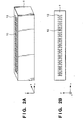
- Figs. 2A and 2B show the practical structure of the waveguide 1.
- Fig. 2A is a schematic perspective view of the waveguide 1.
- Fig. 2B is a plan view of the waveguide 1.
- the slots 10 are arranged in a line such that their longitudinal direction is consistent with the longitudinal direction of the waveguide 1. Electrodes 13 are so formed as to surround these slots 10. In this case, either DC voltage or AC voltage (including RF voltage) may be applied to the electrodes 13.
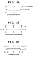
- Figs. 3A to 3C show examples of the arrangement of electrodes 13 formed around an arbitrary slot 10.
- the electrodes 13 are used to ionize a laser gas before microwaves are supplied.
- Fig. 3A shows an example of the arrangement of six electrodes around the slot 10.
- Fig. 3B shows the densities of currents applied to the six electrodes 13.
- J c be the current density at the electrode 13 located near the middle of the slot 10 in the longitudinal direction
- J e be the current density at the electrode 13 located at each end portion of the slot in the longitudinal direction. The current densities are adjusted to meet J c ⁇ J e .
- the densities of electrons generated by preionization have a predetermined distribution. This allows a plasma to be readily excited at each end portion of the slot. That is, the electron density distribution produced by the electrode 13 can compensate for the formation of an electrically ON state in the widthwise direction of the slot 10 upon excitation of a plasma.
- the current density at each end of the slot 10 is set to be higher than that at the central portion of the slot 10.
- the formation of an electron density distribution is not limited to this. An appropriate electron density distribution can be formed by using the electrode 13 in accordance with the operation state.
- a plasma is readily excited near the center of the slot 10 in the longitudinal direction.
- a uniform plasma can be formed over the entire region above the slot 10.
- Figs. 5A to 5C are graphs schematically showing the effects of uniformizing plasma excitation by preionization using the electrode 13.
- Fig. 5A shows, for comparison, the state of plasma excitation in the longitudinal direction of the slot 10 without any electrode 13.
- Fig. 5B is a graph schematically showing an electron density distribution (preionization compensation) in the longitudinal direction of the slot 10 which originates from a current density given to each electrode 13.
- Fig. 5C shows the density of a plasma excited by microwaves emitted from the slot 10 in a case wherein preionization compensation in Fig. 5B is performed by the electrode 13.
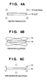
- Figs. 3C and 4A to 4C show other arrangements of the electrodes 13.
- Fig. 3C shows a case wherein the number of electrodes 13 at each end portion of the slot 10 is increased to further facilitate excitation of the laser gas at each end portion of the slot 10. This arrangement allows more effective plasma excitation at each end portion of the slot 10.
- Fig. 4A shows a case wherein the electrodes 13 are formed at only the end portions of the slot 10 while no electrodes 13 are formed at the central portion of the slot 10 at which the laser gas is readily excited.
- the formation of the electrodes 13 only at the end portions of the slot 10, at which the laser gas is not readily excited, ensures a plasma density equal to that at the central portion of the slot 10, thereby uniformizing the plasma density in the entire region above the slot 10.
- Fig. 4B shows a case wherein the electrodes 13 are integrally formed along the longitudinal direction of the slot 10.
- the electron density distribution at each end portion of the slot 10 can be increased by reducing the area of the central portion of each electrode 13 in the longitudinal direction of the slot 10.
- Fig. 4C shows a case wherein the electrodes 13 are located near the slot 10 at each end portion of the slot 10 at which the laser gas is not readily excited.
- Fig. 6 shows an arrangement in which the electrodes 13 are spaced apart from the slot 10.
- efficient preionization can be realized by increasing the current density on the slot 10 side by using reflecting mirrors 14.
- the reflecting mirrors 14 are preferably mounted above the flow path of the laser gas.
- the electrodes 13 are arranged near each slot 10 to increase the electron density at each end portion of the slot 10 in the longitudinal direction as compared with the electron density at the central portion of the slot 10 in the longitudinal direction, thereby promoting excitation of the laser gas at each end portion of the slot 10 in the longitudinal direction, in particular.
- This makes it possible to uniformize a laser gas excitation state (plasma density) in the entire region of the slot 10.
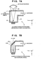
- Figs. 7A and 7B are schematic sectional views each showing a waveguide of an excimer laser oscillating apparatus according to the second embodiment of the present invention.
- the waveguide in the second embodiment is designed to replace the waveguide in the first embodiment, and the overall arrangement of the excimer laser oscillating apparatus is the same as that of the first embodiment.
- the same reference numerals as in the first embodiment denote substantially the same parts in the second embodiment, and a detailed description thereof will be omitted.
- Fig. 7A is a sectional view taken along a direction perpendicular to the longitudinal direction of a waveguide 21.
- the waveguide 21 of the excimer laser oscillating apparatus according to the second embodiment has a substantially L-shaped sectional shape.
- Slots 10 are formed in the lower surface of the waveguide 21.
- a microwave is introduced into the waveguide 21 in the direction indicated by an arrow A in Fig. 7A and emitted into a laser tube 2 through the slot 10, thereby exciting a plasma above the slot 10.
- a UV transmission window 21a is formed at a position opposing the slot 10.
- a UV light source 22 and reflecting mirror 23 are arranged outside the UV transmission window 21a.
- the substantially L-shaped sectional shape of the waveguide 21 makes it possible to directly perform UV irradiation from the position opposing the slot 10.
- the formation of the UV transmission window 21a having a predetermined size can prevent microwaves from leaking through the UV transmission window 21a.
- Fig. 78 is a sectional view taken along a direction perpendicular to the longitudinal direction of a bend waveguide 21'.
- a UV transmission window 21'a is formed in an inclined surface 21'b to allow direct UV irradiation from a position opposing the slot 10 as in the case of the waveguide 21 in Fig. 7A.
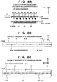
- Fig. 8A is a sectional view taken along the longitudinal direction of the waveguide 21.
- the UV transmission windows 21a are formed along the longitudinal direction of the waveguide 21.
- the UV light sources 22 and reflecting mirrors 23 are arranged in accordance with the positions of the UV transmission windows 21a.
- the UV light sources 22 and reflecting mirrors 23 are so located as to concentrate UV irradiation on the end portions of the slots 10 in the longitudinal direction.
- a reflecting mirror having a spherical surface or any aspherical surface e.g., an elliptic or hyperbolic shape
- a plurality of lenses may be used in place of the reflecting mirror 23, together with a single light source.
- Figs. 8B and 8C show the arrangement of UV transmission windows 21a as a microwave mode which is suited for a case wherein E and H planes are used.
- a wall of a rectangular waveguide which is parallel to an electric field is referred to as an E plane
- a wall of the waveguide which is parallel to a magnetic field is referred to as an H plane.
- an E plane is a long end face of the waveguide
- an H plane is a short end face of the waveguide.
- the UV transmission windows 21a are preferably formed along the longitudinal direction of the slots 10. This arrangement makes it possible to concentrate UV irradiation on the end portions of each slot 10.
- the UV transmission windows 21a are preferably arranged along the longitudinal direction of the slots 10 to be located between the two lines of slots 10.
- transmission windows are preferably arranged for the respective two lines of slots 10 as in the case wherein the E plane is used.
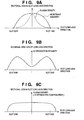
- Figs. 9A to 9C are graphs each schematically showing how plasma excitation is uniformized by UV irradiation.
- Fig. 9A shows a laser gas excitation state (plasma density) without any UV irradiation for comparison.
- Fig. 9B is a graph schematically showing the UV irradiation intensity of the UV light source 22 near the slot 10.
- Fig. 9C shows the laser gas (plasma density) excited by a microwave radiated from the slot 10 when the UV irradiation shown in Fig. 9B is performed.
- excitation of the laser gas at each end portion of the slot 10 in the longitudinal direction in particular, can be promoted.
- a laser gas excitation state (plasma density) in the entire region of the slot 10 can be uniformized.
- the UV light sources 22 are arranged to concentrate UV irradiation on the end portions of the slots 10 in the longitudinal direction, excitation of the laser gas at the end portions of the slots 10, at which the laser gas is not readily excited, can be promoted by UV irradiation.
- This makes it possible to uniformize excitation of the laser gas at the central portion and end portions of each slot 10 in the longitudinal direction, thus uniformly exciting the laser gas in the entire range on each slot 10.
- the same effect as described above can be obtained by using X-ray or RF (Radio Frequency) preionization instead of UV irradiation.
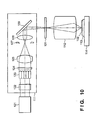
- Fig. 10 is a schematic view showing the main components of this stepper.
- This stepper comprises an illumination optical system 111, projecting optical system 112, wafer chuck 113, .and wafer stage 114.
- the illumination optical system 111 irradiates a reticle 101 on which a desired pattern is drawn with illuminating light.
- the projecting optical system 112 projects the illuminating light (the pattern of the reticle 101) passing through the reticle 101 onto the surface of a wafer 102 in a reduced scale.
- the wafer chuck 113 mounts and fixes the wafer 102.
- the wafer stage 114 fixes the wafer chuck 113. Note that not only a transmission type reticle (reticle 101) shown in Fig. 10 but also a reflection type reticle can be used as a reticle.
- the illumination optical system 111 includes an excimer laser oscillator 121 of the first embodiment, beam shape converter 122, optical integrator 123; stop member 124, condenser lens 125, blind 127, image forming lens 128, and reflecting mirror 129.
- the excimer laser oscillator 121 is a light source for emitting a high-luminance excimer laser beam as illuminating light.
- the beam shape converter 122 converts the illuminating light from the light source 121 into a beam having a desired sectional shape.
- the optical integrator 123 is formed by two-dimensionally arranging a plurality of cylindrical lenses or microlenses.
- the stop member 124 is placed near the position of secondary sources formed by the optical integrator 123 and can be switched to an arbitrary aperture value by a switching mechanism (not shown).
- the condenser lens 125 condenses the illuminating light passing through the stop member 124.
- the blind 127 is constructed of, e.g., four variable blades and placed on the conjugate plane of the reticle 101 to determine an arbitrary illuminating range on the surface of the reticle 101.
- the image forming lens 128 projects the illuminating light formed into a predetermined shape by the blind 127 onto the surface of the reticle 101.
- the reflecting mirror 129 reflects the illuminating light from the image forming lens 128 toward the reticle 101.
- the illuminating light emitted from the light source 121 is converted into a predetermined shape by the beam shape converter 122 and directed to the optical integrator 123. Consequently, a plurality of secondary sources are formed near the exit surface of the optical integrator 123. Illuminating light from these secondary sources is condensed by the condenser lens 125 via the stop member 124 and formed into a predetermined shape by the blind 127. After that, the illuminating light is reflected by the reflecting mirror 229 via the image forming lens 128 and enters the reticle 101. Subsequently, the illuminating light enters the surface of the wafer 102 through the pattern of the reticle 101 and the projection optical system 122. As a consequence, the pattern of the reticle 101 is projected on the wafer 102 in a reduced scale, and the wafer 102 is exposed.
- the exposure apparatus of this embodiment uses the excimer laser oscillator of the first or second embodiment as a laser source. This apparatus can therefore use a high-output and uniform excimer laser beam that can be sustained for a relatively long time period. This allows taped exposure of the wafer 102 with an accurate exposure amount.
- Fig. 11 shows the flow of fabrication steps of semiconductor devices (e.g., semiconductor chips such as ICs and LSIs, liquid crystal panels, or CCDs).
- semiconductor devices e.g., semiconductor chips such as ICs and LSIs, liquid crystal panels, or CCDs.
- step 1 circuit design
- step 2 mask formation
- step 3 wafer fabrication
- step 4 wafer process
- step 5 post-process in which semiconductor chips are formed from the wafers formed in step 4.
- step 6 tests such as an assembly step (dicing and bonding) and a packaging step (chip encapsulation).
- step 6 tests such as an operation test and a durability test are conducted on the semiconductor devices fabricated in step 5.
- the semiconductor devices are completed through these steps and shipped (step 7).
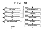
- Fig. 12 shows a detailed flow of the wafer process described above.
- step 11 oxidation
- step 12 CVD
- step 12 conductive films and insulating films are formed on the wafer surfaces by using vapor phase reaction.
- step 13 PVD
- conductive films and insulating films are formed on the wafers by sputtering or vapor deposition.
- step 14 ion implantation
- ions are implanted into the wafers.
- step 15 resist processing
- the wafers are coated with a photosensitive agent.
- step 16 exposure
- the projecting exposure apparatus explained above is used to expose the wafers to the circuit patterns of the mask.
- step 17 development
- step 18 etching
- portions except for the developed resist image are etched away.
- step 19 resist removal
- This fabrication method can easily and reliably fabricate, with high yield, highly integrated semiconductor devices which are conventionally difficult to fabricate.
- a plasma which is uniform as a whole over the length of each slot can be generated. This makes it possible to provide a laser oscillating apparatus capable of uniform laser emission with minimum energy loss, a high-performance exposure apparatus having the laser oscillating apparatus, and a method of fabricating a high-quality device by using the exposure apparatus.
Landscapes
- Physics & Mathematics (AREA)
- Electromagnetism (AREA)
- Engineering & Computer Science (AREA)
- Plasma & Fusion (AREA)
- Optics & Photonics (AREA)
- General Physics & Mathematics (AREA)
- Lasers (AREA)
- Exposure And Positioning Against Photoresist Photosensitive Materials (AREA)
- Exposure Of Semiconductors, Excluding Electron Or Ion Beam Exposure (AREA)
Claims (23)
- Appareil à oscillation laser destiné à générer un faisceau laser en transmettant une onde électromagnétique se propageant dans un guide d'onde (1, 21), dans un tube laser (2) rempli d'un gaz laser, à travers une fente (10) formée dans une paroi dudit guide d'onde, pour exciter le gaz laser, ledit appareil étant caractérisé en ce qu'il comporte :dans lequel ladite partie (13, 21a) d'alimentation en énergie est conçue pour fournir de l'énergie au gaz laser afin d'exciter de façon sensiblement uniforme le gaz laser le long de ladite fente (10).une partie (13, 21a) d'alimentation en énergie destinée à fournir de l'énergie au gaz du laser dans ledit tube laser (2) afin de commander, indépendamment de l'introduction de l'onde électromagnétique à travers ladite fente (10), une distribution d'état d'excitation du gaz laser produite par la transmission de l'onde électromagnétique dans ledit tube laser (2) à travers ladite fente (10) ;
- Appareil selon la revendication 1, caractérisé en ce que ladite partie d'alimentation en énergie comprend, à proximité de ladite fente, une électrode (13) destinée à fournir de l'énergie au gaz laser.
- Appareil selon la revendication 2, caractérisé en ce que ladite partie d'alimentation en énergie peut fonctionner de façon à ioniser le gaz laser en fournissant de l'énergie au gaz laser en utilisant ladite électrode (13).
- Appareil selon l'une quelconque des revendications 1 à 3, caractérisé en ce que ladite partie d'alimentation en énergie peut fonctionner de façon à ioniser de manière préliminaire le gaz laser avant la fourniture d'une onde électromagnétique par l'intermédiaire dudit guide d'onde (1).
- Appareil selon l'une quelconque des revendications 2 à 4, caractérisé en ce que ladite électrode peut fonctionner de façon à fournir de l'énergie au gaz laser afin de rendre une densité d'ionisation, proche d'une partie extrême de ladite fente (10), supérieure à une densité d'ionisation proche d'une position de ladite fente (10).
- Appareil selon la revendication 1, caractérisé en ce que ladite partie d'alimentation en énergie comprend, à proximité de ladite fente (10), au moins une paire d'électrodes (13) destinée à fournir de l'énergie au gaz laser, et ladite, au moins une, paire d'électrodes (13) est agencée de façon à rendre une densité d'ionisation proche d'une partie extrême de ladite fente (10) supérieure à une densité d'ionisation proche d'une partie centrale de ladite fente (10).
- Appareil selon la revendication 1, caractérisé en ce que ladite partie d'alimentation en énergie comprend au moins une paire d'électrodes (13) destinée à fournir de l'énergie au gaz laser, et ladite, au moins une, paire d'électrodes (13) est configurée de façon à rendre une densité de ionisation proche d'une partie extrême de ladite fente (10) supérieure à une densité d'ionisation proche d'une partie centrale de ladite fente (10).
- Appareil selon la revendication 1, caractérisé en ce que ladite partie d'alimentation en énergie comprend, à proximité de ladite fente (10), plusieurs paires d'électrodes (13) destinées à fournir de l'énergie au gaz laser, et un courant, d'une densité de courant supérieure à une densité de courant d'un courant fourni entre ladite paire d'électrodes (13) à proximité d'une partie centrale de ladite fente (10), est fourni entre ladite paire d'électrodes (13) à proximité d'une partie extrême de ladite fente (10).
- Appareil selon la revendication 1, caractérisé en ce que ladite partie d'alimentation en énergie comprend, à proximité de ladite fente (10), une pluralité de paires d'électrodes (13) destinées à fournir de l'énergie au gaz laser, et ladite pluralité de paires d'électrodes (13) se concentre au voisinage d'une partie extrême de ladite fente (10).
- Appareil selon la revendication 1, caractérisé en ce que ladite partie d'alimentation en énergie comprend, le long de ladite fente (10), une paire d'électrodes (13) destinée à fournir de l'énergie au gaz laser, et chacune de ladite paire d'électrodes (13) est plus large au voisinage d'une partie extrême de ladite fente (10) qu'au voisinage d'une partie centrale de ladite fente (10).
- Appareil selon la revendication 1, caractérisé en ce que ladite partie d'alimentation en énergie comprend, à proximité de ladite fente (10), plusieurs paires d'électrodes (13) destinées à fournir de l'énergie au gaz laser, et les électrodes de ladite paire d'électrodes (13) proche d'une partie extrême de ladite fente (10) sont placées plus près de ladite fente (10) que les électrodes de ladite paire d'électrodes (13) proche d'une partie centrale de ladite forme (10).
- Appareil selon l'une quelconque des revendications 1 à 5, caractérisé en ce que ladite partie d'alimentation en énergie est conçue pour fournir de l'énergie au gaz laser afin de rendre une densité d'ionisation proche d'une partie extrême de ladite fente (10) supérieure à une densité d'ionisation proche d'une partie centrale de ladite fente (10).
- Appareil selon la revendication 1, caractérisé en ce que ladite partie d'alimentation en énergie comprend une source de lumière (22) destinée à irradier de lumière une partie proche de ladite fente (10).
- Appareil selon la revendication 13, caractérisé en ce que ledit guide d'onde (21) est placé entre ladite source de lumière (22) et ledit tube laser (2), et une surface dudit guide d'onde (21) comporte une fenêtre (21a) transmettant la lumière provenant de ladite source de lumière (22).
- Appareil selon la revendication (14), caractérisé en ce que la surface du guide d'onde (21) dans laquelle est formée ladite fenêtre (21a) est opposée à une surface dudit guide d'onde (21) dans laquelle est formée ladite fente (10).
- Appareil selon la revendication (14) ou (15), caractérisé en ce que ladite fenêtre (21a) présente une dimension qui empêche le passage de l'onde électromagnétique à travers elle.
- Appareil selon l'une quelconque des revendications 13 à 16, caractérisé en ce que ladite partie d'alimentation en énergie comprend en outre un miroir réfléchissant (23) destiné à réfléchir de la lumière provenant de ladite source de lumière (22) vers une partie proche de ladite fente (10).
- Appareil selon l'une quelconque des revendications 13 à 17, caractérisé en ce que ladite source de lumière (22) génère de la lumière ultraviolette.
- Appareil selon la revendication 1 à 18, caractérisé en ce qu'une pluralité de fentes (10) est formée dans ladite paroi dudit guide d'onde (1).
- Appareil selon la revendication 19, caractérisé en ce que ladite pluralité de fentes (10) est formée suivant une direction longitudinale dudit guide d'onde.
- Appareil selon la revendication 19 ou 20, caractérisé en ce que ladite partie (13) d'alimentation en énergie est prévue pour chaque fente (10).
- Appareil d'exposition comportant une unité à oscillation laser, un système optique d'illumination destiné à illuminer un masque en utilisant de la lumière fournie par ladite unité à oscillation laser, et un système optique de projection destiné à projeter un motif du masque sur un substrat ;
caractérisé en ce que ladite unité à oscillation laser est ledit appareil à oscillation laser défini dans l'une quelconque des revendications 1 à 21. - Procédé de fabrication de dispositifs caractérisé en ce qu'il comprend les étapes qui consistent :à revêtir un substrat d'une matière photosensible ;à exposer un motif sur le substrat revêtu de la matière photosensible en utilisant ledit appareil d'exposition défini dans la revendication 22 ;à développer le motif sur le substrat exposé ; età fabriquer un dispositif à partir du substrat exposé et développé.
Applications Claiming Priority (2)
| Application Number | Priority Date | Filing Date | Title |
|---|---|---|---|
| JP05181499A JP4256520B2 (ja) | 1999-02-26 | 1999-02-26 | レーザ発振装置、露光装置及びデバイスの製造方法 |
| JP5181499 | 1999-02-26 |
Publications (3)
| Publication Number | Publication Date |
|---|---|
| EP1032098A2 EP1032098A2 (fr) | 2000-08-30 |
| EP1032098A3 EP1032098A3 (fr) | 2001-09-12 |
| EP1032098B1 true EP1032098B1 (fr) | 2004-06-09 |
Family
ID=12897383
Family Applications (1)
| Application Number | Title | Priority Date | Filing Date |
|---|---|---|---|
| EP00301521A Expired - Lifetime EP1032098B1 (fr) | 1999-02-26 | 2000-02-25 | Dispositif laser |
Country Status (4)
| Country | Link |
|---|---|
| US (1) | US6650678B1 (fr) |
| EP (1) | EP1032098B1 (fr) |
| JP (1) | JP4256520B2 (fr) |
| DE (1) | DE60011322T2 (fr) |
Families Citing this family (3)
| Publication number | Priority date | Publication date | Assignee | Title |
|---|---|---|---|---|
| DE60023964T2 (de) * | 1999-02-01 | 2006-06-22 | Ohmi, Tadahiro, Sendai | Laservorrichtung, Belichtungsapparat unter Verwendung derselben und Herstellungsverfahren |
| JP3619141B2 (ja) | 2000-11-10 | 2005-02-09 | キヤノン株式会社 | 投影露光装置及びデバイス製造方法 |
| CN101752244B (zh) * | 2001-01-25 | 2012-02-08 | 东京毅力科创株式会社 | 等离子体处理方法 |
Family Cites Families (15)
| Publication number | Priority date | Publication date | Assignee | Title |
|---|---|---|---|---|
| US4004249A (en) * | 1976-01-22 | 1977-01-18 | General Motors Corporation | Optical waveguide laser pumped by guided electromagnetic wave |
| US4802183A (en) * | 1982-04-07 | 1989-01-31 | Board Of Trustees Of The Leland Stanford Junior University | Microwave excited excimer laser and method |
| US4513424A (en) * | 1982-09-21 | 1985-04-23 | Waynant Ronald W | Laser pumped by X-band microwaves |
| DE3912568A1 (de) * | 1989-04-17 | 1990-10-18 | Siemens Ag | Gas-laser, insbesondere co(pfeil abwaerts)2(pfeil abwaerts)-laser |
| DE4112946A1 (de) * | 1991-04-20 | 1992-10-22 | Deutsche Forsch Luft Raumfahrt | Gepulstes gasentladungslasersystem |
| US5255282A (en) * | 1991-11-25 | 1993-10-19 | Quantametrics Inc. | Open waveguide excimer laser |
| US5450436A (en) * | 1992-11-20 | 1995-09-12 | Kabushiki Kaisha Komatsu Seisakusho | Laser gas replenishing apparatus and method in excimer laser system |
| JP3382314B2 (ja) | 1993-08-24 | 2003-03-04 | キヤノン株式会社 | 通信装置及び通信装置の制御方法 |
| US5900103A (en) * | 1994-04-20 | 1999-05-04 | Tokyo Electron Limited | Plasma treatment method and apparatus |
| JP2816813B2 (ja) * | 1994-04-12 | 1998-10-27 | 株式会社小松製作所 | エキシマレーザ装置 |
| JPH08220304A (ja) * | 1995-02-13 | 1996-08-30 | Tadahiro Omi | 光学物品及びそれを用いた露光装置又は光学系並びにその製造方法 |
| US5696428A (en) * | 1995-06-07 | 1997-12-09 | Lsi Logic Corporation | Apparatus and method using optical energy for specifying and quantitatively controlling chemically-reactive components of semiconductor processing plasma etching gas |
| JP3815578B2 (ja) * | 1996-07-19 | 2006-08-30 | 忠弘 大見 | エキシマレーザー発振装置 |
| US6331994B1 (en) | 1996-07-19 | 2001-12-18 | Canon Kabushiki Kaisha | Excimer laser oscillation apparatus and method, excimer laser exposure apparatus, and laser tube |
| WO1998033362A1 (fr) * | 1997-01-29 | 1998-07-30 | Tadahiro Ohmi | Dispositif a plasma |
-
1999
- 1999-02-26 JP JP05181499A patent/JP4256520B2/ja not_active Expired - Lifetime
-
2000
- 2000-02-24 US US09/512,075 patent/US6650678B1/en not_active Expired - Lifetime
- 2000-02-25 EP EP00301521A patent/EP1032098B1/fr not_active Expired - Lifetime
- 2000-02-25 DE DE60011322T patent/DE60011322T2/de not_active Expired - Lifetime
Also Published As
| Publication number | Publication date |
|---|---|
| DE60011322D1 (de) | 2004-07-15 |
| DE60011322T2 (de) | 2005-06-23 |
| EP1032098A2 (fr) | 2000-08-30 |
| EP1032098A3 (fr) | 2001-09-12 |
| JP2000252565A (ja) | 2000-09-14 |
| JP4256520B2 (ja) | 2009-04-22 |
| US6650678B1 (en) | 2003-11-18 |
Similar Documents
| Publication | Publication Date | Title |
|---|---|---|
| KR100347826B1 (ko) | 엑시머레이저발진장치및방법,엑시머레이저노광장치,그리고레이저관 | |
| EP0066053B1 (fr) | Dispositif et procédé pour l'exposition à la lumière d'un milieu photosensible | |
| JP2002006096A (ja) | 電磁波発生装置、これを用いた半導体製造装置並びに半導体デバイスの製造方法 | |
| US6690702B1 (en) | Excimer laser oscillation apparatus and method, excimer laser exposure apparatus, and laser tube | |
| US6829279B1 (en) | Laser oscillating apparatus, exposure apparatus using the same and device fabrication method | |
| US6744802B1 (en) | Laser oscillating apparatus with slotted waveguide | |
| US6650678B1 (en) | Laser oscillating apparatus | |
| JPH10163547A (ja) | 連続発光エキシマレーザ発振装置及び発振方法、露光装置並びにレーザ管 | |
| EP1039595B1 (fr) | Laser à gaz | |
| JP4256519B2 (ja) | レーザ発振装置、露光装置及びデバイスの製造方法 | |
| JP4204689B2 (ja) | レーザ発振装置、露光装置及びデバイスの製造方法 | |
| US6903354B2 (en) | Extreme ultraviolet transition oscillator | |
| US6885015B2 (en) | Thermionic-cathode for pre-ionization of an extreme ultraviolet (EUV) source supply | |
| JP4295855B2 (ja) | レーザ発振装置、露光装置及びデバイスの製造方法 | |
| JP4256518B2 (ja) | レーザ発振装置、露光装置及びデバイスの製造方法 | |
| JP4302810B2 (ja) | レーザ発振装置、露光装置及びデバイスの製造方法 | |
| JP2000252563A (ja) | レーザ発振装置、露光装置及びデバイスの製造方法 | |
| JPH10163553A (ja) | 連続発光エキシマレーザ発振装置及び発振方法、露光装置並びにレーザ管 | |
| KR20040020585A (ko) | 플라즈마 반응기를 이용한 극자외선 발생 장치 및 방법 | |
| JPH11354862A (ja) | エキシマレーザ発振装置及び発振方法、露光装置並びにレーザ管 | |
| JPH11204857A (ja) | エキシマレーザ発振装置及び発振方法、露光装置並びにレーザ管 | |
| JPH11168264A (ja) | 露光方法および露光装置ならびに半導体集積回路装置の製造方法 | |
| JPH0612755B2 (ja) | 露光装置 |
Legal Events
| Date | Code | Title | Description |
|---|---|---|---|
| PUAI | Public reference made under article 153(3) epc to a published international application that has entered the european phase |
Free format text: ORIGINAL CODE: 0009012 |
|
| AK | Designated contracting states |
Kind code of ref document: A2 Designated state(s): DE GB NL Kind code of ref document: A2 Designated state(s): AT BE CH CY DE DK ES FI FR GB GR IE IT LI LU MC NL PT SE |
|
| AX | Request for extension of the european patent |
Free format text: AL;LT;LV;MK;RO;SI |
|
| PUAL | Search report despatched |
Free format text: ORIGINAL CODE: 0009013 |
|
| AK | Designated contracting states |
Kind code of ref document: A3 Designated state(s): AT BE CH CY DE DK ES FI FR GB GR IE IT LI LU MC NL PT SE |
|
| AX | Request for extension of the european patent |
Free format text: AL;LT;LV;MK;RO;SI |
|
| 17P | Request for examination filed |
Effective date: 20020128 |
|
| 17Q | First examination report despatched |
Effective date: 20020423 |
|
| AKX | Designation fees paid |
Free format text: DE GB NL |
|
| GRAP | Despatch of communication of intention to grant a patent |
Free format text: ORIGINAL CODE: EPIDOSNIGR1 |
|
| RIN1 | Information on inventor provided before grant (corrected) |
Inventor name: SUZUKI, NOBUMASA,C/O CANON KABUSHIKI KAISHA Inventor name: SHINOHARA, TOSHIKUNI,C/O CANON KABUSHIKI KAISHA Inventor name: TANAKA, NOBUYOSHIC/O CANON KABUSHIKI KAISHA Inventor name: OHMI, TADAHIRO Inventor name: OHSAWA, HIROSHI,C/O CANON KABUSHIKI KAISHA Inventor name: HIRAYAMA, MASAKI,C/O CANON KABUSHIKI KAISHA |
|
| RIN1 | Information on inventor provided before grant (corrected) |
Inventor name: HIRAYAMA, MASAKI Inventor name: SHINOHARA, TOSHIKUNI Inventor name: TANAKA, NOBUYOSHIC/O CANON KABUSHIKI KAISHA Inventor name: OHSAWA, HIROSHI,C/O CANON KABUSHIKI KAISHA Inventor name: OHMI, TADAHIRO Inventor name: SUZUKI, NOBUMASA,C/O CANON KABUSHIKI KAISHA |
|
| GRAS | Grant fee paid |
Free format text: ORIGINAL CODE: EPIDOSNIGR3 |
|
| GRAA | (expected) grant |
Free format text: ORIGINAL CODE: 0009210 |
|
| AK | Designated contracting states |
Kind code of ref document: B1 Designated state(s): DE GB NL |
|
| REG | Reference to a national code |
Ref country code: GB Ref legal event code: FG4D |
|
| RIN1 | Information on inventor provided before grant (corrected) |
Inventor name: SHINOHARA, TOSHIKUNI Inventor name: TANAKA, NOBUYOSHIC/O CANON KABUSHIKI KAISHA Inventor name: SUZUKI, NOBUMASA,C/O CANON KABUSHIKI KAISHA Inventor name: OHMI, TADAHIRO Inventor name: OHSAWA, HIROSHI,C/O CANON KABUSHIKI KAISHA Inventor name: HIRAYAMA, MASAKI |
|
| REF | Corresponds to: |
Ref document number: 60011322 Country of ref document: DE Date of ref document: 20040715 Kind code of ref document: P |
|
| PLBE | No opposition filed within time limit |
Free format text: ORIGINAL CODE: 0009261 |
|
| STAA | Information on the status of an ep patent application or granted ep patent |
Free format text: STATUS: NO OPPOSITION FILED WITHIN TIME LIMIT |
|
| 26N | No opposition filed |
Effective date: 20050310 |
|
| PGFP | Annual fee paid to national office [announced via postgrant information from national office to epo] |
Ref country code: DE Payment date: 20190212 Year of fee payment: 20 Ref country code: NL Payment date: 20190116 Year of fee payment: 20 Ref country code: GB Payment date: 20190220 Year of fee payment: 20 |
|
| REG | Reference to a national code |
Ref country code: DE Ref legal event code: R071 Ref document number: 60011322 Country of ref document: DE |
|
| REG | Reference to a national code |
Ref country code: NL Ref legal event code: MK Effective date: 20200224 |
|
| REG | Reference to a national code |
Ref country code: GB Ref legal event code: PE20 Expiry date: 20200224 |
|
| PG25 | Lapsed in a contracting state [announced via postgrant information from national office to epo] |
Ref country code: GB Free format text: LAPSE BECAUSE OF EXPIRATION OF PROTECTION Effective date: 20200224 |