EP1032120A2 - Leistungsverstärker, Leistungsregelungsverfahren für einen Leistungsverstärker und kommunikationsgerät - Google Patents
Leistungsverstärker, Leistungsregelungsverfahren für einen Leistungsverstärker und kommunikationsgerät Download PDFInfo
- Publication number
- EP1032120A2 EP1032120A2 EP00103893A EP00103893A EP1032120A2 EP 1032120 A2 EP1032120 A2 EP 1032120A2 EP 00103893 A EP00103893 A EP 00103893A EP 00103893 A EP00103893 A EP 00103893A EP 1032120 A2 EP1032120 A2 EP 1032120A2
- Authority
- EP
- European Patent Office
- Prior art keywords
- amplifier
- terminal
- frequency switch
- fet
- switch circuit
- Prior art date
- Legal status (The legal status is an assumption and is not a legal conclusion. Google has not performed a legal analysis and makes no representation as to the accuracy of the status listed.)
- Withdrawn
Links
Images







Classifications
-
- H—ELECTRICITY
- H03—ELECTRONIC CIRCUITRY
- H03F—AMPLIFIERS
- H03F1/00—Details of amplifiers with only discharge tubes, only semiconductor devices or only unspecified devices as amplifying elements
- H03F1/02—Modifications of amplifiers to raise the efficiency, e.g. gliding Class A stages, use of an auxiliary oscillation
- H03F1/0205—Modifications of amplifiers to raise the efficiency, e.g. gliding Class A stages, use of an auxiliary oscillation in transistor amplifiers
- H03F1/0277—Selecting one or more amplifiers from a plurality of amplifiers
-
- H—ELECTRICITY
- H03—ELECTRONIC CIRCUITRY
- H03F—AMPLIFIERS
- H03F1/00—Details of amplifiers with only discharge tubes, only semiconductor devices or only unspecified devices as amplifying elements
- H03F1/02—Modifications of amplifiers to raise the efficiency, e.g. gliding Class A stages, use of an auxiliary oscillation
- H03F1/0205—Modifications of amplifiers to raise the efficiency, e.g. gliding Class A stages, use of an auxiliary oscillation in transistor amplifiers
- H03F1/0288—Modifications of amplifiers to raise the efficiency, e.g. gliding Class A stages, use of an auxiliary oscillation in transistor amplifiers using a main and one or several auxiliary peaking amplifiers whereby the load is connected to the main amplifier using an impedance inverter, e.g. Doherty amplifiers
-
- H—ELECTRICITY
- H03—ELECTRONIC CIRCUITRY
- H03F—AMPLIFIERS
- H03F3/00—Amplifiers with only discharge tubes or only semiconductor devices as amplifying elements
- H03F3/72—Gated amplifiers, i.e. amplifiers which are rendered operative or inoperative by means of a control signal
-
- H—ELECTRICITY
- H03—ELECTRONIC CIRCUITRY
- H03F—AMPLIFIERS
- H03F2203/00—Indexing scheme relating to amplifiers with only discharge tubes or only semiconductor devices as amplifying elements covered by H03F3/00
- H03F2203/72—Indexing scheme relating to gated amplifiers, i.e. amplifiers which are rendered operative or inoperative by means of a control signal
- H03F2203/7239—Indexing scheme relating to gated amplifiers, i.e. amplifiers which are rendered operative or inoperative by means of a control signal the gated amplifier being switched on or off by putting into parallel or not, by choosing between amplifiers and shunting lines by one or more switch(es)
Definitions
- the present invention relates to a power amplifier, a control method for such a power amplifier, and a communication equipment which are used mainly in a mobile communication system.
- CDMA Code Division Multiple Access
- Fig 13. is a diagram showing the configuration of power amplifier of the convention art. Referring to Fig. 13, 701 denotes an input terminal, 702 denotes a preamplifier, 703 denotes a postamplifier, and 704 denotes an output terminal.
- Fig. 14 is a graph showing a consumed current, an amount of distortion, and an efficiency with respect to an output power of the power amplifier of the conventional art.
- the solid lines show variations of characteristics in the case where the initial currents are set to be similar to set values in a power amplifier of a conventional digital portable telephone of the TDMA system, and the broken lines show characteristics in the case where the initial currents of the preamplifier and the postamplifier shown in Fig. 13 are set to be a half of the values.
- a power amplifier is controlled so that efficiency at maximum output becomes maximum.
- the power output is controlled in such wide range of exceeding 70 dB from maximum output in accordance with the distance between a telephone and a base station. Therefore it is demanded to satisfy high efficiency for whole power output range.
- the initial currents of the power amplifier are to be set as smallest within tolerable amount of distortion.
- the initial current may be set to be close to that of Class B (the initial current is reduced in level). In this case, however, the distortion level is impaired. Therefore, the reduction of the initial current is limited.
- the invention has been conducted in view of the problems of the power amplifier of the conventional art. It is an object of the invention to provide a power amplifier the efficiency of which is not impaired even in the CDMA system, and a control method for the power amplifier.
- the power amplifier of the present invention comprises: an input terminal; an output terminal; an N number of bypassable amplification circuits which are connected directly or indirectly in a sequential manner between said input terminal and said output terminal; an impedance conversion circuit which is connected directly or indirectly between said amplification circuit of a final stage and said output terminal; and a bias control circuit which controls said amplification circuits,
- a power amplifier of the present invention comprises: an input terminal; a first high-frequency switch circuit which can output a signal input to said input terminal while switching to two output terminals; a first amplifier which is connected directly or indirectly to one of said output terminals of said first high-frequency switch circuit; a second high-frequency switch circuit which is connected directly or indirectly to an output terminal of said first amplifier and another one of said output terminals of said first high-frequency switch circuit, and which can independently output two signals respectively input from said output terminals while switching to two output terminals a second amplifier which is connected directly or indirectly to one of said output terminals of said second high-frequency switch circuit; an impedance conversion circuit which is connected directly or indirectly to another one of said output terminals of said second high-frequency switch circuit; an output terminal which is commonly connected directly or indirectly to an output terminal of said second amplifier and an output terminal of said impedance conversion circuit; and a bias control circuit which controls power source voltages of said first and second amplifiers and controls status of said switch circuit.
- a power amplifier of the present invention comprises: an input terminal; a first high-frequency switch circuit which can output a signal input to said input terminal while switching to two output terminals; a first amplifier which is connected directly or indirectly to one of said output terminals of said first high-frequency switch circuit; a second high-frequency switch circuit which is connected directly or indirectly to an output terminal of said first amplifier and another one of said output terminals of said first high-frequency switch circuit, and which can independently output two signals respectively input from said output terminals while switching to two output terminals; a second amplifier which is connected directly or indirectly to one of said output terminals of said second high-frequency switch circuit; a third high-frequency switch circuit which is connected directly or indirectly to an output terminal of said second amplifier and another one of said output terminals of said second high-frequency switch circuit, and which can independently output two signals respectively input from said output terminals while switching to two output terminals; a third amplifier which is connected directly or indirectly to one of said output terminals of said third high-frequency switch circuit; an impedance conversion circuit which is connected directly or indirectly to another
- a power amplifier of the present invention comprises: an input terminal; a first high-frequency switch circuit which can output a signal input to said input terminal while switching to two output terminals; a first amplifier which is connected directly or indirectly to one of said output terminals of said first high-frequency switch circuit; impedance switching means which is connected directly or indirectly to an output terminal of said first amplifier; a second high-frequency switch circuit which is connected directly or indirectly to another one of said output terminals of said first high-frequency switch circuit and an output terminal of said impedance switching means, and which can independently output two signals respectively input from said output terminals while switching to three output terminals; a first final amplifier which is connected directly or indirectly to a first one of said output terminals of said second high-frequency switch circuit; a second final amplifier which is connected directly or indirectly to a second one of said output terminals of said second high-frequency switch circuit; a impedance conversion circuit which is connected directly or indirectly to a third one of said output terminals of said second high-frequency switch circuit; an output terminal which is commonly connected directly or indirectly to said
- a power control method of the present invention for a power amplifier comprising: at least two stages of power amplifiers; a bypass circuit which is connected in parallel to said power amplifiers; a high-frequency switch circuit which is connected to input/output terminals of said power amplifiers and said bypass circuit, and a bias control circuit, is such method that
- the amplifier of a higher power is bypassed by a high-frequency switch, and the power source of the bypassed amplifier is cut off, whereby the efficiency in transmission at a low power can be improved.
- the amplifier in front of the bypassed amplifier is bypassed, and the power source of the newly bypassed amplifier is cut off, thereby further improving the efficiency.
- the final amplifier is bypassed by a bypass circuit using a high-frequency switch to cut off the bias current of a final transistor, thereby enabling the efficiency to be improved.
- the initial current of the amplifier itself of each stage is reduced so that the amplifier operates in a manner similar to that of Class B, whereby the efficiency at a low output power can be improved.
- predistortion compensation is performed by using transistors of the high-frequency switch in the bypass circuit. Therefore, a power amplifier can be realized in which the initial current is low in level and an unnecessary current is interrupted at a low output power can be realized without increasing the circuit scale.
- Fig. 1 is a block diagram of a power amplifier of the first embodiment.
- the reference numeral 100 denotes a bias control circuit
- 101 denotes an input terminal
- 102 denotes a first high-frequency switch circuit which switches one input to two outputs
- 103 denotes a preamplifier
- 104 denotes a second high-frequency switch circuit which independently switches two inputs to two outputs
- 105 denotes a postamplifier
- 106 denotes a quarter wavelength line (impedance conversion circuit)
- 107 denotes an output terminal.
- the amplification circuit 1010 according to the invention is a combination of the high-frequency switch circuits and the amplifiers.
- connection between A and B is made in the first high-frequency switch circuit 102, and connection between C and D is made in the second switch.
- the impedance of a terminal E of the second switch is short-circuited (or set to be low), whereby the impedance when seeing the terminal E from an output terminal of the postamplifier 105 via the quarter wavelength line 106 is converted into open (high impedance).
- Fig. 1, 1000 denotes a switch for causing the short circuit.
- a signal which is input via the input terminal 101 is amplified by the preamplifier 103, and then further amplified by the postamplifier 105.
- An output signal of the postamplifier is output to the output terminal 107.
- connection between C and E is made in the second high-frequency switch circuit 104 while maintaining the connection between A and B in the first high-frequency switch circuit 102 of Fig. 1.
- the bias current of the postamplifier 105 is then interrupted by the bias control circuit 100.
- the bias control circuit performs the bias control so that the impedance when seeing the output of the postamplifier 105 from the point where the quarter wavelength line 106 is connected to the output terminal 107 is set to be high.
- the signal which is input via the input terminal 101 is amplified by the preamplifier 103, and then bypasses around the postamplifier 105 to be transmitted to the output terminal 107 via the quarter wavelength line 106.
- connection between A and F is made in the first high-frequency switch circuit 102, and connection between G and E is made in the second high-frequency switch circuit 102.
- the bias currents of the preamplifier 103 and the postamplifier 105 are then interrupted by the bias control circuit 100. Therefore, the signal which is input via the input terminal 101 bypasses around the preamplifier 103 and the postamplifier 105 to be transmitted to the output terminal 107.
- Fig. 2 shows variations of the consumed current with respect to the output power of the power amplifier.
- the power amplifier operates as described above, the power amplifier has consumed current characteristics indicated by the thick line in Fig. 2(a). Namely, the consumed current can be largely reduced as compared with the case where the amplifiers are not bypassed.
- PMAX indicates the maximum transmission power
- PLEV1 indicates “PMAX - the gain of the postamplifier”
- PLEV2 indicates "PLEV1 - the gain of preamplifier”.
- the value of the power at which the transmission power is reduced and the bypassing operation is started may be shifted from that of the power at which the transmission power is increased and the bypassing operation is stopped. In this configuration, the switching frequency of the bypassing operation can be reduced.
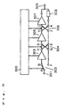
- Fig. 3 is a block diagram of a power amplifier of the second embodiment.
- the reference numeral 300 denotes a bias control circuit
- 301 denotes an input terminal
- 302 denotes a first high-frequency switch circuit which switches one input to two outputs
- 303 denotes a preamplifier
- 304 denotes a second high-frequency switch circuit which independently switches two inputs to two outputs
- 305 denotes a middle amplifier
- 306 denotes a third high-frequency switch circuit which independently switches two inputs to two outputs
- 307 denotes a postamplifier
- 308 denotes a quarter wavelength line
- 309 denotes an output terminal.
- the power amplifier of the second embodiment of the invention is configured by: the input terminal 301; the first high-frequency switch circuit 302 which switches a signal input via the input terminal 301 to two outputs; the first amplifier (preamplifier) 303 which is connected to one of the outputs of the first high-frequency switch circuit 302; the second high-frequency switch circuit 304 which independently switches two inputs respectively connected to an output of the first amplifier 303 and the other output of the first high-frequency switch circuit 302, to two outputs; the second amplifier (middle amplifier) 305 which is connected to one of the outputs of the second high-frequency switch circuit 304; the third high-frequency switch circuit 306 which independently switches two inputs respectively connected to an output of the second amplifier 305 and the other output of the second high-frequency switch circuit 304, to two outputs; the third amplifier (postamplifier) 307 which is connected to one of the outputs of the third high-frequency switch circuit 306; the quarter wavelength line 308 which is connected to the other output of the third high-frequency switch circuit 306;
- the first embodiment is modified so that the bypass circuit is expanded to an amplifier of a lower transmission power.
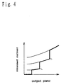
- the consumed current can be reduced as shown in Fig. 4.
- amplification circuits 1010 (combinations of a high-frequency switch circuit and an amplifier) can be connected at any N stages.
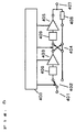
- Fig. 5 is a block diagram of a power amplifier of the third embodiment.
- the reference numeral 400 denotes a bias control circuit
- 401 denotes an input terminal
- 402 denotes a first high-frequency switch circuit which switches one input to two outputs
- 403 denotes a preamplifier
- 404 denotes a second high-frequency switch circuit which independently switches two inputs to two outputs
- 405 denotes a postamplifier
- 406 denotes a quarter wavelength line
- 407 denotes an output terminal
- 408 denotes a first predistortion circuit which previously compensates distortion generated in the preamplifier
- 409 denotes a second predistortion circuit which previously compensates distortion generated in the postamplifier.
- the power amplifier of the third embodiment of the invention is characterized in that, in addition to the configuration of the first embodiment, the first predistortion circuit (first predistortion compensation circuit) 408 is disposed between the first high-frequency switch circuit 402 and the first amplifier (preamplifier) 403, and the second predistortion circuit (second predistortion compensation circuit) 409 is disposed between the second high-frequency switch circuit 404 and the second amplifier (postamplifier) 405.
- the first and second predistortion circuits of Fig. 5 previously correct one or both of amplitude distortion and phase distortion of the preamplifier and the postamplifier, whereby nonlinear distortion of the whole of the amplifier can be reduced.
- the initial currents of the amplifiers can be reduced by an amount corresponding to the improved degree of the distortion. In this case, even in a range where the bypass circuit is not switched, reduction of the consumed current in a reduced transmission power can be realized. It is a matter of course that an unnecessary current can be reduced by the bias control same as that described in the first embodiment.
- the predistortion compensation circuits are placed in front of the first and second amplifiers, respectively. Even when a predistortion compensation circuit is used only for one of the amplifiers, it is possible to reduce nonlinear distortion of the whole of the amplifier.
- predistortion compensation circuits are used in the configuration of the power amplifier of the first embodiment. Also when predistortion compensation circuits are used in the power amplifier of the second embodiment, nonlinear distortion of the whole of the amplifier can be similarly reduced.
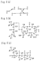
- FIG. 6 is a block diagram of a power amplifier of the fourth embodiment.
- Fig. 6 shows the high-frequency switch circuit of the first embodiment.
- (a) is a block diagram of the circuit
- (b) is a diagram of the circuit
- (c) is a diagram of a circuit which is an improvement of the circuit of (b)
- a to E denote terminals of the high-frequency switch circuit.
- each of transistors Q1 to Q8 in Fig. 6(c), and transistors Q1 to Q12 in Fig. 6(b) is shown in a state where the gate terminal is opened. Actually, however, the gate terminal is connected to the bias control circuit via a serial protection resistor and a parallel bypass capacitor for reducing noise components.
- the number of transistors can be decreased by four as compared with the switch configuration of (b), and therefore the circuit can be miniaturized, thereby enabling the circuit to be easily integrated into an IC.
- the high-frequency switch circuit shown in Fig. 6(c) comprises: the first input terminal A; the first transistor Q2 in which one of the drain and the source is connected in series to the first input terminal A, the first output terminal B being connected to the other one of the drain and the source of the first transistor Q2, one of the drain and the source of the second transistor Q1 in which the other one of the drain and the source is grounded in a high-frequency manner being connected to the first output terminal B; the third transistor Q3 in which one of the drain and the source is connected in series to the first input terminal A, the second output terminal E being connected to the other one of the drain and the source of the third transistor Q3, one of the drain and the source of the fourth transistor Q4 in which the other one of the drain and the source is grounded in a high-frequency manner being connected to the second output terminal E; the fifth transistor Q5 in which one of the drain and the source is connected in series to the second output terminal E, the second input terminal C being connected to the other one of the drain and the source of the fifth transistor Q5, one of the
- the effects of the third embodiment can be attained without adding a special predistortion circuit.
- the effects of the third embodiment can be attained without involving a special predistortion circuit.
- FIG. 7 is a block diagram of a power amplifier of the fifth embodiment.
- Fig. 7 shows the high-frequency switch circuit of the second embodiment.
- (a) is a block diagram of the circuit
- (b) is a diagram of the circuit
- a to K denote terminals of the switch circuit.
- each of transistors Q1 to Q14 in Fig. 7(b) is shown in a state where the gate terminal is opened. Actually, however, the gate terminal is connected to the bias control circuit via a serial protection resistor and a parallel bypass capacitor for reducing noise components.
- the number of transistors in the circuit can be decreased by six as compared with the conventional configuration, and the circuit can be miniaturized, thereby enabling the circuit to be easily integrated into an IC.
- the conventional configuration is for example such circuit that the circuit part of Q1 to Q11 in Fig. 6(b) is added to the whole circuit of the Fig. 6(b) while the output terminal E is connected with the input terminal of said added part circuit.
- the number of the transistors in the conventional configuration is 20 but the Fig. 7(b) is only 14 and the six transistors can be reduced.
- the high-frequency switch circuit shown in Fig. 7(b) comprises: the first input terminal A; the first transistor Q2 in which one of the drain and the source is connected in series to the first input terminal A, the first output terminal B being connected to the other one of the drain and the source of the first transistor Q2, one of the drain and the source of the second transistor Q1 in which the other one of the drain and the source is grounded in a high-frequency manner being connected to the first output terminal B; the third transistor Q3 in which one of the drain and the source is connected in series to the first input terminal A, one of the drain and the source of the fourth transistor Q4 in which the other one of the drain and the source is grounded in a high-frequency manner being connected to the other one of the drain and the source of the third transistor Q3; the fifth transistor Q5 in which one of the drain and the source is connected in series to the other one of the drain and the source of the third transistor Q3, the second input terminal C being connected to the other one of the drain and the source of the fifth transistor Q5, one of the drain and the source
- the effects of the third embodiment can be attained without involving a predistortion circuit.
- the effects of the third embodiment can be attained without involving a predistortion circuit.
- the effects of the third embodiment can be attained without involving a predistortion circuit.
- Fig. 8 is a block diagram of a power amplifier 600 according to the invention.
- the reference numeral 601 denotes an input terminal
- 602 denotes a first high-frequency switch which switches one input to two outputs
- 603 denotes an amplifier
- 604 denotes impedance switching means
- 605 denotes a second high-frequency switch which switches two inputs to three outputs
- 606 denotes a first final amplifier
- 607 denotes a second final amplifier
- 608 denotes a transmission line
- 609 denotes an output terminal
- 610 denotes a bias control circuit.
- the power amplifier of the sixth embodiment causes the first high-frequency switch 601 of Fig. 8 to make connection between A and B, and the second high-frequency switch 605 to make connection among C, D, and E.
- the impedance of a terminal F of the second high-frequency switch 605 is short-circuited to be lowered, by closing a switch 1001, whereby the impedance when seeing the terminal from outputs of the first and second final amplifiers 606 and 607 via the transmission line 608 is converted into an open-circuit impedance (high impedance).
- a signal which is input via the input terminal 601 is amplified by the amplifier 603, and then further amplified by the first and second final amplifiers 606 and 607. Output signals of the final amplifiers are output to the output terminal 609.
- the first and second final amplifiers 606 and 607 are connected to each other in parallel and the circuits have usually the same characteristic impedance, matching is attained by using the impedance switching means 604.
- connection between C and D is made in the second high-frequency switch 605 while maintaining the connection between A and B in the first high-frequency switch 602.
- the control circuit 610 performs a control so that the bias current of the second final amplifier 607 is interrupted, a bias is given so as to set the impedance when seeing the output of the second final amplifier 607 from the point where the first final amplifier 606 is connected to the output terminal 609 to be high, and the impedance switching means 604 is turned off. Therefore, the signal which is input via the input terminal 601 is amplified by the amplifier 603, the amplified signal is further amplified by the first final amplifier 606, and an output signal of the amplifier is output to the output terminal 609.
- connection between C and E is made in the second high-frequency switch 605 while maintaining the connection between A and B in the first high-frequency switch 602.
- the control circuit 610 performs a control so that the bias current of the second final amplifier 607 is interrupted, a bias is given so as to set the impedance when seeing the output of the first final amplifier 606 from the point where the second final amplifier 607 is connected to the output terminal 609 to be high, and the impedance switching means 604 is turned off. Therefore, the signal which is input via the input terminal 601 is amplified by the amplifier 603, the amplified signal is further amplified by the second final amplifier 607, and an output signal of the amplifier is output to the output terminal 609.
- connection between C and F is made in the second high-frequency switch 605 while maintaining the connection between A and B in the first high-frequency switch 602.
- the control circuit 610 performs a control so that the bias currents of the first and second final amplifiers 606 and 607 are interrupted, a bias is given so as to set the impedances when seeing the outputs of the first second final amplifiers 606 and 607 from the point where the transmission line 608 is connected to the output terminal 609 to be high, and the impedance switching means 604 is turned off. Therefore, the signal which is input via the input terminal 601 is amplified by the amplifier 603, and the amplified signal bypasses around the final amplifiers 606 and 607, and then output to the output terminal 609 via the transmission line 608.
- connection between A and G is made in the first switch 602, and connection between H and F is made in the second switch 605.
- the control circuit 610 performs a control so that the bias currents of the first and second final amplifiers 606 and 607 are interrupted, a bias is given so as to set the impedances when seeing the outputs of the first second final amplifiers 606 and 607 from the point where the transmission line 608 is connected to the output terminal 609 to be high, and the impedance switching means 604 is turned off. Therefore, the signal which is input via the input terminal 601 bypasses around the amplifier 603 and the final amplifiers, and then output to the output terminal 609 via the transmission line 608.
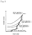
- Fig. 9 shows variations of the consumed current with respect to the output power of the power amplifier of the sixth embodiment in the case where the first and second final amplifiers 606 and 607 have different characteristics.
- the power amplifier When the power amplifier operates as described above, the power amplifier has consumed current characteristics indicated by the thick line in Fig. 9. Namely, the consumed current can be largely reduced as compared with the case where the amplifiers are not bypassed.
- the efficiency at an output power which is lower by 3 dB than the maximum output power may be made equal to that at the maximum output power.
- the value of the transmission power at the timing of the bypass switching in the case where the transmission power is increasing may be shifted from that in the case where the transmission power is decreasing, whereby the switching frequency of the bypass switching operation can be reduced.
- Fig. 10 shows the switches_ in Fig. 8 showing the power amplifier of the sixth embodiment.
- (a) is a block diagram of the switches
- (b) is a circuit diagram of the switches.
- the symbols of the terminals correspond to those of Fig. 8.
- each of transistors Q1 to Q10 in Fig. 10(b) is shown in a state where the gate terminal is opened. Actually, however, the gate terminal is connected to the control circuit via a serial protection resistor and a parallel bypass capacitor for reducing noise components.
- the high-frequency switch circuit shown in Fig. 10(b) comprises: the first input terminal A; the first transistor Q2 in which one of the drain and the source is connected in series to the first input terminal A, the first output terminal B being connected to the other one of the drain and the source of the first transistor Q2, one of the drain and the source of the second transistor Q1 in which the other one of the drain and the source is grounded in a high-frequency manner being connected to the first output terminal B; the third transistor Q3 in which one of the drain and the source is connected in series to the first input terminal A, the second output terminal F being connected the other one of the drain and the source of the third transistor Q3, one of the drain and the source of the fourth transistor Q4 in which the other one of the drain and the source is grounded in a high-frequency manner being connected to the second output terminal F; the fifth transistor Q5 in which one of the drain and the source is connected in series to the second output terminal F, the second input terminal C being connected to the other one of the drain and the source of the fifth transistor Q5, one of the drain
- the power amplifier is enabled to perform a predistortion operation without involving a predistortion circuit.
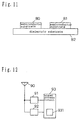
- the above-mentioned high-frequency switch circuits are configured on a first same semiconductor substrate 80, the amplifiers are configured on a second same semiconductor substrate 81, and the first and second semiconductor substrates 80 and 81 are mounted on a same dielectric substrate 82.
- the communication equipment of the invention is a communication equipment which is characterized in that the equipment comprises: a power amplifier 931 according to the invention which has been described above; an antenna 90; a reception circuit 91; a signal process circuit 93 which processes a signal from the reception circuit 91 by using the power amplifier 931; and a transmission circuit 92 which performs a transmission process on a signal supplied from the signal process circuit 93.
- the amplifier of a higher power is bypassed by the high-frequency switch, and the power source of the bypassed amplifier is cut off, whereby the efficiency in transmission at a low power can be improved.
- the efficiency can be improved in a broad dynamic range in transmission.
- the initial current of the amplifier itself of each stage is reduced so that the amplifier operates in a manner similar to that of Class B, whereby the efficiency at a low output power can be improved.
- predistortion compensation is performed by using transistors of the high-frequency switch in the bypass circuit. Therefore, a power amplifier can be realized in which the initial current is low in level and an unnecessary current is interrupted at a low output power can be realized without increasing the circuit scale.
Landscapes
- Engineering & Computer Science (AREA)
- Power Engineering (AREA)
- Amplifiers (AREA)
Applications Claiming Priority (4)
| Application Number | Priority Date | Filing Date | Title |
|---|---|---|---|
| JP4999599 | 1999-02-26 | ||
| JP4999599 | 1999-02-26 | ||
| JP28957999 | 1999-10-12 | ||
| JP28957999 | 1999-10-12 |
Publications (2)
| Publication Number | Publication Date |
|---|---|
| EP1032120A2 true EP1032120A2 (de) | 2000-08-30 |
| EP1032120A3 EP1032120A3 (de) | 2003-07-30 |
Family
ID=26390428
Family Applications (1)
| Application Number | Title | Priority Date | Filing Date |
|---|---|---|---|
| EP00103893A Withdrawn EP1032120A3 (de) | 1999-02-26 | 2000-02-24 | Leistungsverstärker, Leistungsregelungsverfahren für einen Leistungsverstärker und kommunikationsgerät |
Country Status (2)
| Country | Link |
|---|---|
| US (1) | US6329875B1 (de) |
| EP (1) | EP1032120A3 (de) |
Cited By (14)
| Publication number | Priority date | Publication date | Assignee | Title |
|---|---|---|---|---|
| EP1229642A1 (de) * | 2001-01-31 | 2002-08-07 | Sony International (Europe) GmbH | Leistungsverstärker zum Verstärken von Funksignalen |
| WO2002065649A3 (en) * | 2001-01-25 | 2002-11-07 | Ericsson Telefon Ab L M | Amplifier phase change compensation |
| WO2003007473A1 (de) * | 2001-07-12 | 2003-01-23 | Kathrein-Werke Kg | Verstärkerumschaltung |
| WO2003032680A2 (en) | 2001-10-04 | 2003-04-17 | Koninklijke Philips Electronics N.V. | Transponder with a changeable circuit configuration |
| WO2002029970A3 (en) * | 2000-10-06 | 2003-09-25 | Tropian Inc | Variable bias control for switch mode rf amplifier |
| EP1345322A4 (de) * | 2000-12-15 | 2004-12-15 | Matsushita Electric Industrial Co Ltd | Leistungsverstaerker und kommunikationsgeraet |
| EP1612932A1 (de) * | 2004-06-23 | 2006-01-04 | Wavics, Inc. | Verstärker mit Vielfach-Leistungsmodus und mit der Möglichkeit der Vorspannungsmodulation und ohne Bypass-Schaltungen |
| US7161422B2 (en) | 2003-01-03 | 2007-01-09 | Junghyun Kim | Multiple power mode amplifier with bias modulation option and without bypass switches |
| US7554392B2 (en) | 2007-04-24 | 2009-06-30 | Avago Technologies Wireless Ip (Singapore) Pte. Ltd. | Multiple output power mode amplifier |
| US7616054B2 (en) | 2007-01-09 | 2009-11-10 | Avago Technologies Wireless Ip (Singapore) Pte. Ltd. | Multiple output power mode amplifier |
| US7623896B2 (en) * | 2004-02-04 | 2009-11-24 | Sharp Kabushiki Kaisha | Wireless communication circuit and wireless communication apparatus using the same |
| WO2010014984A3 (en) * | 2008-08-01 | 2010-04-15 | Qualcomm Incorporated | Multi-mode configurable transmitter circuit |
| EP2523346A1 (de) * | 2011-05-09 | 2012-11-14 | Alcatel Lucent | Verstärker mit schaltbaren Verstärkerstufen sowie Verfahren |
| WO2014029807A1 (en) * | 2012-08-21 | 2014-02-27 | Nokia Siemens Networks Oy | High efficiency power amplifier architecture for off-peak traffic hours |
Families Citing this family (9)
| Publication number | Priority date | Publication date | Assignee | Title |
|---|---|---|---|---|
| DE60035598T2 (de) * | 2000-10-27 | 2008-06-19 | Stmicroelectronics N.V. | Verfahren und Vorrichtung zur Leistungsregelung eines Mobilfunktelefons |
| US20040224649A1 (en) * | 2003-02-05 | 2004-11-11 | Khosro Shamsaifar | Electronically tunable power amplifier tuner |
| US7385447B1 (en) * | 2004-06-28 | 2008-06-10 | Anadigics, Inc. | Power amplifier having curve-fitting predistorter |
| US7489910B2 (en) * | 2005-03-30 | 2009-02-10 | Kabushiki Kaisha Toshiba | Wireless transmitter and amplifier |
| TWI318498B (en) * | 2006-05-08 | 2009-12-11 | Novatek Microelectronics Corp | Variable gain amplifying circuit and method of changing the gain amplifying path |
| US7768353B2 (en) | 2008-06-13 | 2010-08-03 | Samsung Electro-Mechanics Company, Ltd. | Systems and methods for switching mode power amplifier control |
| US8643433B2 (en) * | 2011-06-30 | 2014-02-04 | Broadcom Corporation | Bypass power amplifier for improving efficiency at low power |
| KR102163049B1 (ko) * | 2015-02-24 | 2020-10-08 | 삼성전기주식회사 | 전력 증폭기 및 전력 증폭기의 출력 제어 방법 |
| US10361733B2 (en) * | 2017-12-13 | 2019-07-23 | At&T Intellectual Property I, L.P. | Low complexity transmitter structure for active antenna systems |
Family Cites Families (14)
| Publication number | Priority date | Publication date | Assignee | Title |
|---|---|---|---|---|
| US4315222A (en) * | 1980-03-06 | 1982-02-09 | Bell Telephone Laboratories, Incorporated | Power combiner arrangement for microwave amplifiers |
| JPH0653753A (ja) | 1992-07-29 | 1994-02-25 | Nec Corp | 電力増幅装置 |
| JPH07115331A (ja) | 1993-10-19 | 1995-05-02 | Mitsubishi Electric Corp | 増幅装置 |
| JP3444653B2 (ja) | 1994-06-09 | 2003-09-08 | 三菱電機株式会社 | 電力増幅器 |
| US5661434A (en) * | 1995-05-12 | 1997-08-26 | Fujitsu Compound Semiconductor, Inc. | High efficiency multiple power level amplifier circuit |
| JPH09135127A (ja) * | 1995-11-07 | 1997-05-20 | Nec Corp | 電力増幅器 |
| JPH1032441A (ja) | 1996-07-15 | 1998-02-03 | Hitachi Denshi Ltd | 電力増幅器 |
| US5786727A (en) * | 1996-10-15 | 1998-07-28 | Motorola, Inc. | Multi-stage high efficiency linear power amplifier and method therefor |
| US5973557A (en) * | 1996-10-18 | 1999-10-26 | Matsushita Electric Industrial Co., Ltd. | High efficiency linear power amplifier of plural frequency bands and high efficiency power amplifier |
| JPH10173453A (ja) * | 1996-12-09 | 1998-06-26 | Sony Corp | 高周波可変利得増幅装置および無線通信装置 |
| JPH118560A (ja) * | 1997-04-25 | 1999-01-12 | Matsushita Electric Ind Co Ltd | 送信出力制御回路及び送信出力制御方法 |
| JPH10327082A (ja) | 1997-05-23 | 1998-12-08 | Saitama Nippon Denki Kk | 移動無線機の送信増幅回路 |
| JP3171141B2 (ja) * | 1997-06-06 | 2001-05-28 | 日本電気株式会社 | 移動体通信用送信機およびその制御方法 |
| JP3387508B2 (ja) * | 1998-02-19 | 2003-03-17 | 株式会社エヌ・ティ・ティ・ドコモ | 無線送信増幅装置 |
-
2000
- 2000-02-24 EP EP00103893A patent/EP1032120A3/de not_active Withdrawn
- 2000-02-28 US US09/514,777 patent/US6329875B1/en not_active Expired - Lifetime
Cited By (31)
| Publication number | Priority date | Publication date | Assignee | Title |
|---|---|---|---|---|
| WO2002029970A3 (en) * | 2000-10-06 | 2003-09-25 | Tropian Inc | Variable bias control for switch mode rf amplifier |
| CN100409565C (zh) * | 2000-10-06 | 2008-08-06 | 松下电器产业株式会社 | 用于开关模式rf放大器的可变偏压控制 |
| EP1345322A4 (de) * | 2000-12-15 | 2004-12-15 | Matsushita Electric Industrial Co Ltd | Leistungsverstaerker und kommunikationsgeraet |
| US6960959B2 (en) | 2000-12-15 | 2005-11-01 | Matsushita Electric Industrial Co., Ltd. | Power amplifier and communication apparatus |
| WO2002065649A3 (en) * | 2001-01-25 | 2002-11-07 | Ericsson Telefon Ab L M | Amplifier phase change compensation |
| US6909884B2 (en) | 2001-01-25 | 2005-06-21 | Telefonaktiebolaget Lm Ericsson (Publ) | Amplifier phase change compensation |
| EP1229642A1 (de) * | 2001-01-31 | 2002-08-07 | Sony International (Europe) GmbH | Leistungsverstärker zum Verstärken von Funksignalen |
| WO2003007473A1 (de) * | 2001-07-12 | 2003-01-23 | Kathrein-Werke Kg | Verstärkerumschaltung |
| US7064604B2 (en) | 2001-07-12 | 2006-06-20 | Kathrein-Werke Kg | Amplifier switch |
| CN100401633C (zh) * | 2001-07-12 | 2008-07-09 | 凯瑟雷恩工厂两合公司 | 冗余放大器切换电路 |
| WO2003032680A2 (en) | 2001-10-04 | 2003-04-17 | Koninklijke Philips Electronics N.V. | Transponder with a changeable circuit configuration |
| EP1440601A2 (de) * | 2001-10-04 | 2004-07-28 | Koninklijke Philips Electronics N.V. | Transponder mit veränderbarer schaltungskonfiguration |
| US7388427B2 (en) | 2003-01-03 | 2008-06-17 | Avago Technologies General Ip (Singapore) Pte. Ltd. | Multiple power mode amplifier with bias modulation option and without bypass switches |
| US7315205B2 (en) | 2003-01-03 | 2008-01-01 | Junghyun Kim | Multiple power mode amplifier with bias modulation option and without bypass switches |
| US7394313B2 (en) | 2003-01-03 | 2008-07-01 | Avago Technologies General Ip (Singapore) Pte. Ltd | Multiple power mode amplifier with bias modulation option and without bypass switches |
| US7161422B2 (en) | 2003-01-03 | 2007-01-09 | Junghyun Kim | Multiple power mode amplifier with bias modulation option and without bypass switches |
| US7348841B2 (en) | 2003-01-03 | 2008-03-25 | Junghyun Kim | Multiple power mode amplifier with bias modulation option and without bypass switches |
| US7420412B2 (en) | 2003-01-03 | 2008-09-02 | Junghyun Kim | Multiple power mode amplifier with bias modulation option and without bypass switches |
| US7623896B2 (en) * | 2004-02-04 | 2009-11-24 | Sharp Kabushiki Kaisha | Wireless communication circuit and wireless communication apparatus using the same |
| EP1612932A1 (de) * | 2004-06-23 | 2006-01-04 | Wavics, Inc. | Verstärker mit Vielfach-Leistungsmodus und mit der Möglichkeit der Vorspannungsmodulation und ohne Bypass-Schaltungen |
| US7616054B2 (en) | 2007-01-09 | 2009-11-10 | Avago Technologies Wireless Ip (Singapore) Pte. Ltd. | Multiple output power mode amplifier |
| US7714647B2 (en) | 2007-01-09 | 2010-05-11 | Avago Technologies Wireless Ip (Singapore) Pte. Ltd. | Multiple output power mode amplifier |
| US7554392B2 (en) | 2007-04-24 | 2009-06-30 | Avago Technologies Wireless Ip (Singapore) Pte. Ltd. | Multiple output power mode amplifier |
| WO2010014984A3 (en) * | 2008-08-01 | 2010-04-15 | Qualcomm Incorporated | Multi-mode configurable transmitter circuit |
| US8099127B2 (en) | 2008-08-01 | 2012-01-17 | Qualcomm Incorporated | Multi-mode configurable transmitter circuit |
| CN102113222B (zh) * | 2008-08-01 | 2015-03-25 | 高通股份有限公司 | 多模式可配置发射器电路 |
| CN104660276A (zh) * | 2008-08-01 | 2015-05-27 | 高通股份有限公司 | 多模式可配置发射器电路 |
| CN104660276B (zh) * | 2008-08-01 | 2019-11-19 | 高通股份有限公司 | 多模式可配置发射器电路 |
| EP2523346A1 (de) * | 2011-05-09 | 2012-11-14 | Alcatel Lucent | Verstärker mit schaltbaren Verstärkerstufen sowie Verfahren |
| WO2014029807A1 (en) * | 2012-08-21 | 2014-02-27 | Nokia Siemens Networks Oy | High efficiency power amplifier architecture for off-peak traffic hours |
| US8742842B2 (en) | 2012-08-21 | 2014-06-03 | Nokia Siemens Networks Oy | High efficiency power amplifier architecture for off-peak traffic hours |
Also Published As
| Publication number | Publication date |
|---|---|
| EP1032120A3 (de) | 2003-07-30 |
| US6329875B1 (en) | 2001-12-11 |
Similar Documents
| Publication | Publication Date | Title |
|---|---|---|
| US6329875B1 (en) | Power amplifier, power control method for power amplifier, and communication equipment | |
| US5878331A (en) | Integrated circuit | |
| US6118343A (en) | Power Amplifier incorporating single drain switch and single negative voltage generator | |
| US7053706B2 (en) | High linearity doherty communication amplifier with bias control | |
| EP0687060B1 (de) | Leistungsverstärker | |
| US20200336107A1 (en) | Multi-mode stacked amplifier | |
| JP3103712B2 (ja) | 電力増幅器及び増幅方法 | |
| JP3877558B2 (ja) | 高周波電力増幅器、高周波電力増幅器モジュール及び携帯電話機 | |
| US6996376B2 (en) | Antenna switch | |
| US6812794B1 (en) | Multistage amplifier | |
| KR20010053413A (ko) | 이동체 전화 장치 | |
| WO2006088589A2 (en) | Power control circuit for accurate control of power amplifier output power | |
| CN105490648A (zh) | 一种多模功率放大器及其应用 | |
| JP4001818B2 (ja) | 直交低ノイズ増幅器を備えるフロントエンド及び高周波受信器 | |
| US10972051B2 (en) | Power amplifier circuit | |
| WO2005043747A2 (en) | High linearity doherty communication amplifier with bias control | |
| KR20230105034A (ko) | 차동 구조를 이용하는 2단 도허티 전력 증폭 장치 및 이의 제어 방법 | |
| CN111769840B (zh) | 具有多种工作模式的射频信号处理电路和射频前端单元 | |
| CN115774468B (zh) | 一种可调自适应偏置结构 | |
| WO2002058230A1 (en) | Intelligent switching mode power amplifying apparatus | |
| JP2001185957A (ja) | 電力増幅器、電力増幅器の電力制御方法及び通信機器 | |
| KR100487347B1 (ko) | 고효율 전력 증폭기 | |
| KR100347213B1 (ko) | 이동 통신 장비용 알에프 전력 증폭기 | |
| JPH09186533A (ja) | 伝送装置 | |
| KR100531373B1 (ko) | 전력 증폭기 |
Legal Events
| Date | Code | Title | Description |
|---|---|---|---|
| PUAI | Public reference made under article 153(3) epc to a published international application that has entered the european phase |
Free format text: ORIGINAL CODE: 0009012 |
|
| AK | Designated contracting states |
Kind code of ref document: A2 Designated state(s): AT BE CH CY DE DK ES FI FR GB GR IE IT LI LU MC NL PT SE |
|
| AX | Request for extension of the european patent |
Free format text: AL;LT;LV;MK;RO;SI |
|
| PUAL | Search report despatched |
Free format text: ORIGINAL CODE: 0009013 |
|
| AK | Designated contracting states |
Designated state(s): AT BE CH CY DE DK ES FI FR GB GR IE IT LI LU MC NL PT SE |
|
| AX | Request for extension of the european patent |
Extension state: AL LT LV MK RO SI |
|
| AKX | Designation fees paid | ||
| REG | Reference to a national code |
Ref country code: DE Ref legal event code: 8566 |
|
| STAA | Information on the status of an ep patent application or granted ep patent |
Free format text: STATUS: THE APPLICATION IS DEEMED TO BE WITHDRAWN |
|
| 18D | Application deemed to be withdrawn |
Effective date: 20040131 |